2020 ANNUAL SYMPOSIUM - FLORIDA CHAPTER OF THE AVS SCIENCE AND TECHNOLOGY SOCIETY - AVS.org
←
→
Page content transcription
If your browser does not render page correctly, please read the page content below
2020 ANNUAL SYMPOSIUM

            FLORIDA CHAPTER
                  OF
THE AVS SCIENCE AND TECHNOLOGY SOCIETY

             March 9 & 10, 2020
         University of Central Florida
         Engineering Building Atrium
              Orlando, Florida
                       1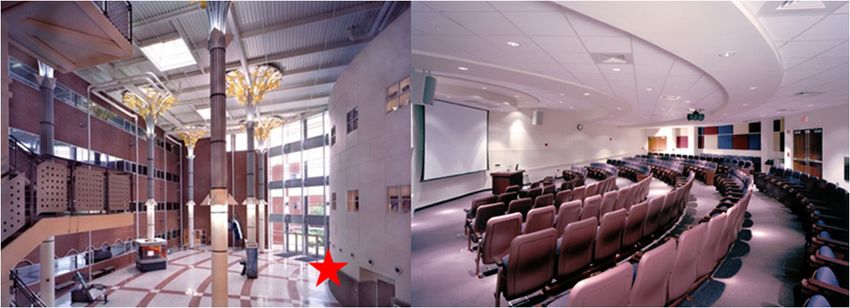
INSTITUTIONAL SPONSORSHIP

We gratefully acknowledge the following centers and
     institutional offices for their sponsorship
                 of our symposium

                         2
All Scientific

    3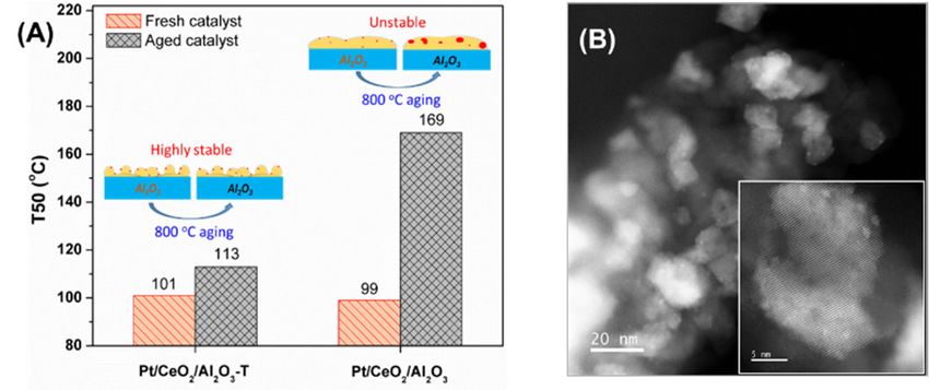
SYMPOSIUM PROGRAM

Monday, March 9, 2020
8:30am – 5:00pm    Registration                 Registration Desk

8:30am – 5:00pm    Student Poster Setup         Engineering Atrium

8:30am – 10:30am   Equipment Exhibit Setup      Engineering Atrium

9:15am – 6:00pm    Technical Program            ENG II Room 102

6:00pm – 8:00pm    Poster Session               Engineering Atrium

6:00pm – 8:00pm    Reception                    Engineering Atrium

Tuesday, March 10, 2020
9:30am – 5:00pm    Technical Program            ENG II Room 102

12:45pm – 1:00pm   Door Prize Drawing           Engineering Atrium

5:00pm – 5:30pm    Poster Awards                Engineering Atrium

5:30pm – 6:30pm    Poster & Exhibit Breakdown   Engineering Atrium

                                    4
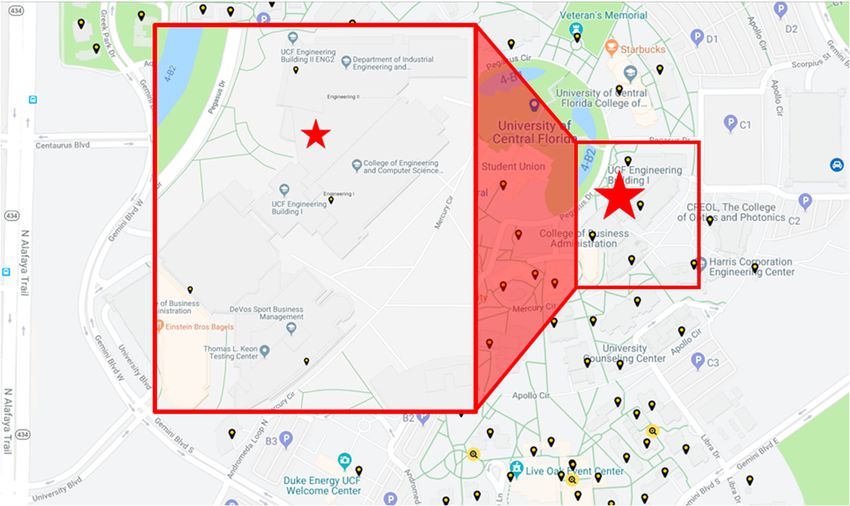
MEETING LOCATION

                          UCF Engineering Building
                            12760 Pegasus Drive
                             Orlando, FL 32816

                       Inside UCF Engineering Building
                 Atrium and Adjacent Presentation Room (102)

Parking in Garage D

                                      5
Monday, March 9, 2020

Opening remarks
9:00am-9:15am
Engineering II Building, Room 102
Program Chair: Prof. Mihai E. Vaida, University of Central Florida

Renewable Energy
9:15am-11:00am        Chair: Prof. Kristopher Davis, University of Central Florida

9:15-9:45   Invited Speaker – Prof. Wolfgang Sigmund, University of Florida
            Materials Needs in Energy Engineering in the 21st Century
9:45-10:15 Invited Speaker – Dr. Sonali Das, University of Central Florida
            Biomimetic light trapping schemes for thin and flexible solar cells
10:15-10:45 Invited Speaker – Dr. Paul Brooker, Orlando Utilities Commission
            for the DOE Solar Energy Innovators Program
            Addressing the Impact of High Penetration Solar PV on the Electric Grid
10:45-11:15 Invited Speaker – Dr. J.G. Newman, Physical Electronics
            Analysis of Inorganic Materials by TOF-SIMS MS/MS

11:15am-11:30am       Coffee Break & Exhibit

Keynote Address
11:30am-12:30pm
                                     Prof. Henry Hess
                 Department of Biomedical Engineering, Columbia University
                 Engineering with biomolecular motors and enzyme cascades

12:30pm-12:40pm       Group picture
12:40pm-1:30pm        Lunch break & Exhibit

Electronic Materials and Photonics
1:30pm-3:30pm         Chair: Prof. Hebin Li, Florida International University

1:30-2:00     Invited Speaker – Prof. Jin He, Florida International University
              Probing chemical interaction and reaction at single-molecule level in a plasmonic
              molecular junction
2:00-2:30     Invited Speaker – Prof. Andreas Muller, University of South Florida
              Microgravity-enhanced Raman scattering for chemical gas sensing
2:30-3:00     Invited Speaker – Prof. Dmitry Voronin, University of South Florida
              Quantum Biophotonics with 2D Materials
3:00-3:30     Invited Speaker – Prof. Daniel F. Santavicca, University of North Florida
              Hybrid Nanopatterning Techniques Utilizing Chemical Self-Assembly

                                               6
3:30pm-3:45pm        Coffee Break & Exhibit

Thin Films and 2D Materials
3:45pm-6:00pm        Chair: Prof. Humberto R. Gutiérrez, University of South Florida

3:45- 4:15    Invited Speaker – Prof. Yeonwoong Jung, University of Central Florida
              Wafer-Scale Integrations of 2D TMD Heterostructures of Controlled Layer
              Orientation on Arbitrary Substrates: Towards Mechanically-Reconfigurable
              Electronic Devices
4:15- 4:45    Invited Speaker – Prof. Darío A. Arena, University of South Florida
              Spin Dynamics in Metallic and Insulating Thin Films Probed with Low and High
              Energy Photons
4:45 - 5:15   Invited Speaker – Prof. Lilia M. Woods, University of South Florida
              Bilayered van der Waals structures: a platform for novel electronic properties
5:15 - 5:45   Invited Speaker – Dr. Kinga Lasek, University of South Florida
              Surface science studies of MBE grown transition metal ditellurides
5:45 - 6:00   Contributed Talk – Sajeevi Withanage, University of Central Florida
              Effect of growth conditions on the electrical properties of large area CVD grown
              MoS2 thin films

Poster Session and Reception
6:00pm-8:00pm        Chair: Prof. Laurene Tetard, Prof. Mihai Vaida, University of Central
                     Florida

                                              7
Tuesday, March 10, 2020
Surface Science and Catalysis
9:30am-12:15pm Chair: Prof. Fudong Liu, University of Central Florida
9:30-9:45 Contributed Talk – Shaohua Xie, University of Central Florida
Highly Active and Stable Platinum Catalyst on Improved Metal Oxide Support for
Efficient CO Oxidation
9:45-10:00 Contributed Talk – Brian C. Ferrari, University of Central Florida
Electron irradiation of astrophysical ice analogues: implications for the
formations of biomolecules on Enceladus
10:00-10:15 Contributed Talk – Sharad Ambardar, University of South Florida
Nano-optical imaging of monolayer MoSe2 and WS2
10:15-10:30 Contributed Talk – Fernand Eliud Torres-Davila, University of Central Florida
Exploring the photochemical properties of defect-laden hexagonal Boron Nitride
10:30-11:00 Invited Speaker – Prof. Shengqian Ma, University of South Florida
Development of Metal-Organic Frameworks as a Versatile Platform for
Heterogeneous Catalysis
11:00am-11:15am Coffee break & Exhibit
11:15-11:45 Invited Speaker – Prof. Jason F. Weaver, University of Florida
Surface chemistry of rutile IrO2(110)
11:45-12:15 Invited Speaker – Prof. Rudolf J. Wehmschulte, Florida Institute of Technology
Catalysis with “naked” cations
12:15pm-1:15pm Lunch break & Exhibit
Meet in Atrium for Door Prize Drawing at 12:45pm
Nanometer-scale Materials, Science, and Technology
1:15pm-3:00pm Chair: Prof. Brent Gila, University of Florida
1:15-1:45 Invited Speaker – Prof. Sergey Stolbov, University of Central Florida
Tuning the Catalyst Surface Electronic Structure to Strengthen Binding for One
Reactants while Weaken It for the Others.
1:45-2:15 Invited Speaker – Prof. Xiaofeng Feng, University of Central Florida
Rational Design of Metal Nanocatalysts for Electrochemical Fuel Synthesis
2:15-2:30 Contributed Talk – Md Afjal Khan Pathan, University of Central Florida
Ultrafast molecular dynamics of CD3I on insulating and semiconducting oxide
surfaces
2:30-2:45 Contributed Talk – Sachit Shah, University of Central Florida
Polyelectrolyte complex micelle encapsulation for the delivery of therapeutics
2:45-3:00 Contributed Talk – Asim Khaniya, University of Central Florida Electron
surface scattering and resistivity of epitaxial Ru(0001) Films
83:00pm-3:15pm Coffee Break & Exhibit
Young Leaders Session
3:15pm-4:35pm Chair: Prof. William Kaden, University of Central Florida
3:15-3:35 Bijoya Dhar, University of Central Florida
D2O-TPD study on 2D aluminosilicate thin films
3:35-3:55 Corbin Feit, University of Central Florida
Near-zero temperature coefficient of resistivity (NZ-TCR) of ALD TiXSiYNZ films
3:55-4:15 Avra Kundu, University of Central Florida
Precision Vascular Delivery of Agrochemicals with Micromilled Microneedles
4:15-4:35 Naseem Ud Din, University of Central Florida
Design of Redox active Metal Organic Chains for single site catalysis using
First-principles density functional theory
Careers in Vacuum Science and Technology
4:35pm-5:35pm Chair: Prof. William Kaden, University of Central Florida
Poster Session Awards & Symposium Conclusions
5:35pm-6:00pm Chair: Prof. Mihai Vaida, University of Central Florida
9Monday, March 9, 2020
Keynote Address
Engineering with biomolecular motors and enzyme cascades
Henry Hess
Department of Biomedical Engineering, Columbia University
Motor proteins, including kinesin, can serve as biological components in engineered
nanosystems. A proof-of-principle application is a “smart dust” biosensor for the remote
detection of biological and chemical agents. The development of this system requires the
integration of a diverse set of technologies, illustrates the complexity of biophysical mechanisms,
and enables the formulation of general principles for nanoscale engineering. Molecular motors
also introduce an interesting new element into self-assembly processes by accelerating transport,
reducing unwanted connections, and enabling the formation of non-equilibrium structures. The
formation of nanowires and nanospools from microtubules transported by kinesin motors
strikingly illustrates these aspects of motor-driven self-assembly. Our most recent work created a
molecular system that is capable of dynamically assembling and disassembling its building
blocks while retaining its functionality, and demonstrates the possibility of self- healing and
adaptation. In our system, filaments (microtubules) recruit biomolecular motors (kinesins) to a
surface engineered to allow for the reversible binding of the kinesin motors. These recruited
motors perform the function of propelling the microtubules along the surface. When the
microtubules leave the kinesin motors behind, the kinesin track can either disassemble and
release the motors back into solution with the possibility of being reassembled into another track,
or recruit other microtubules onto itself, reinforcing the track and thus creating a molecular ‘ant
trail’.
Secondly, the observed enhancement of the throughput of enzymatic cascades on scaffolds will
be discussed. A proximity effect has been invoked to explain the enhanced activity of enzyme
cascades on DNA scaffolds. Using the cascade reaction carried out by glucose oxidase and
horseradish peroxidase as a model system, we studied the kinetics of the cascade reaction when
the enzymes are free in solution, when they are conjugated to each other and when a competing
enzyme is present. No proximity effect was found, which is in agreement with models predicting
that the rapidly diffusing hydrogen peroxide intermediate is well mixed. We suggest that the
reason for the activity enhancement of enzymes localized by DNA scaffolds is that the pH near
the surface of the negatively charged DNA nanostructures is lower than that in the bulk solution,
creating a more optimal pH environment for the anchored enzymes. Our findings challenge the
notion of a proximity effect and provide new insights into the role of scaffolds and of the enzyme
environment.
10Sessions
Renewable Energy
Chair: Prof. Kristopher Davis, University of Central Florida
9:15am-9:45am:
Materials Needs in Energy Engineering in the 21st Century
Wolfgang Sigmund
Department of Materials Science and Engineering, University of Florida
This talk will provide an overview of some of the challenges as well as highlight advances in the
development of novel energy engineering technologies and materials. About 300 years ago
humans started to use fossil fuels in ever larger quantities. This plus other actions by mankind
caused a human contribution of about 120 ppm of CO2 to the atmospheric concentration. In 1897
Svante Arrhenius already estimated what impact an increase of carbonic acid in the air could
have on the planet’s temperatures. Today we still depend heavily on fossil fuels and experience
the effects of global warming more and more. Therefore, novel directions in materials and
technology development are most important, and some universities have even created “Green
Energy Engineering Departments” or centers. The focus for materials is on improvements in
energy harvesting, conversion and storage. Furthermore, carbon or emission negative
technologies are needed to combat the global challenge of increasing emissions.
Towards global sustainability: Education on environmentally clean energy technologies, Janusz
Nowotny, John Dodson, Sebastian Fiechter, Turgut M Gür, Brendan Kennedy, Wojciech Macyk,
Tadeusz Bak, Wolfgang Sigmund, Michio Yamawaki, Kazi A Rahman, Renewable and
Sustainable Energy Reviews, 81, 2541-2551, 2018 Defect chemistry and defect engineering of
TiO2-based semiconductors for solar energy conversion, Janusz Nowotny, Mohammad Abdul
Alim, Tadeusz Bak, Mohammad Asri Idris, Mihail Ionescu, Kathryn Prince, Mohd Zainizan
Sahdan, Kamaruzzaman Sopian, Mohd Asri Mat Teridi, Wolfgang Sigmund, Chemical Society
Reviews, 44 (23), 8424-8442, 2015.
Electronic property dependence of electrochemical performance for TiO2/CNT core-shell
nanofibers in lithium ion batteries, R Qing, L Liu, H Kim, WM Sigmund, Electrochimica Acta,
180, 295-306, 2015.
119:45am-10:15am:
Biomimetic light trapping schemes for thin and flexible solar cells
Sonali Das
Department of Electrical and Computer Engineering, University of Central Florida
The primary scaling factor in photovoltaics is the reduction of the active absorber thickness.
Reducing the crystalline silicon absorber thickness (approx. 3 - 40 um) offers advantages of
reduced material cost, along with mechanical flexibility and light weight opening a new regime
of applications in flexible and wearable electronics. But silicon at such thicknesses suffers from
low photon absorption in the solar spectrum. To compensate for the low light absorption in such
thin substrates, light trapping and light management schemes become essential. The challenge
when applying such schemes to photovoltaics is the need to provide broadband, omnidirectional
solutions to problems. Over millions of years, nature has evolved with various biomimetic
nanostructures which offer broadband responses to reducing reflection and enhancing light-
trapping. Biomimetics in solar cells is enabled by engineering the silicon surface to form
nanopillars, nanowires etc., which decreases the reflection loss and allows more light to couple
into the silicon substrate. The structured silicon absorber increases surface area and surface
recombination, which is detrimental to the solar cell efficiency. Thus, it is imperative to use a
light trapping scheme devoid of silicon structuring to enhance the photo-conversion efficiency.
All-dielectric leaf inspired biomimetic light-trapping scheme on planar graphene/silicon
Schottky junction solar cells with the use of bottom layer of titania spheres and top layer of silica
spheres suppresses reflection over wide angles of incidence and increases absorption in active
silicon layer over AM1.5G solar spectrum and therefore the efficiency. The inherent mechanical
flexibility of graphene along with the lucrative properties of high electron mobility and
transparency, makes it suitable for integration with thin flexible non-structured planar crystalline
silicon substrates for extraction of the photogenerated carriers. An optimal silicon thickness
coupled with an engineered light trapping scheme leads to efficient electron-photon harvesting.
After continuous bending and straightening, the ultra-thin solar cell can retain its performance,
revealing the excellent stability and flexibility of the device. Such simple, low-cost light trapping
schemes are universal.
1210:15am-10:45am:
Addressing the Impact of High Penetration Solar PV on the Electric Grid
Paul Brooker,
Orlando Utilities Commission for the DOE Solar Energy Innovators Program
Due to declining costs, solar photovoltaic (solar PV) adoption rates are rapidly increasing, both
in distributed and utility applications. This influx of renewable energy sources will introduce
challenges to grid operators across multiple time scales. For instance, rapid fluctuations from
large-scale PV arrays can cause power plants to cycle significantly more than their initial designs
predicted. High penetration PV within the distribution network could cause a decrease in
transformer lifetimes and require much more frequent replacements. Addressing these challenges
is necessary in order to ensure an electric grid with high reliability and power quality. This
presentation will highlight the issues presented by large-adoption rates of solar PV, as well as
technologies and approaches that may be leveraged to address these issues.
10:45am-11:15am:
Analysis of Inorganic Materials by TOF-SIMS MS/MS
G.L. Fisher1, S. Iida2, D. M. Carr1, A. A. Ellsworth1 and S.R. Bryan1, J.G. Newman1
1
Physical Electronics, 18725 Lake Dr. East, Chanhassen, MN 55317
2
ULVAC-PHI, 2500 Hagisono, Chigasaki, Kanagawa, 253-8522, Japan
jnewman@phi.com
While the unique and powerful application of Time-of-Flight Secondary Ion Mass Spectrometry
(TOF-SIMS) for the identification of organic materials may be well known, its use for the
analysis of inorganic materials is somewhat less common. However, TOF-SIMS’ attributes of
high surface sensitivity, excellent detection limits, small analytical probe size, detection of all
elements and their isotopes including hydrogen, the ability to easily analyze insulators, and its
molecular information content make it an excellent choice for studying inorganic heterogenous
catalyst surfaces. Of special importance is its ability to detect and map the spatial distributions
of very low concentration (ppm levels) elements of alkali and alkaline earths often used as
catalysis promoters. These promoters can be at concentrations difficult, if not impossible, to
detect with other surface analysis techniques such as Auger Electron Spectroscopy (AES) or X-
ray Photoelectron Spectroscopy (XPS).
This presentation describes the current state of the art of TOF-SIMS instrumentation and how
new improvements including tandem mass spectrometry can be used to help identify the
localized molecular structure of inorganic materials.
13Electronic Materials and Photonics
Chair: Prof. Hebin Li, Florida International University
1:30pm-2:00pm:
Probing chemical interaction and reaction at single-molecule level in a
plasmonic molecular junction
Jin He
Physics Department, Biomolecular Science Institute,
Florida International University, Miami, FL 33199, USA
Measurements at the single-molecule level can reveal the dynamics, intermediates, stochastics
and heterogeneity in the chemical reaction and interactions. We have formed plasmonic
junctions by utilizing the individual collision events of gold nanoparticle (GNP) at a gold
nanoelectrode (GNE). By modifying molecules to the GNP and GNE surfaces, the nanogap
between GNP and GNE becomes a versatile nanoscale chemical reactor. We can monitor
chemical changes in the junction at the single-molecule level using surface enhanced Raman
spectroscopy (SERS). The chemical interaction and reactions can be catalyzed and modulated by
laser irradiation, electrochemical potential and environment. In this talk, I will show a few
examples of interactions and reactions we have probed, including hydrogen bonding and host-
guest interactions.
2:00pm-2:30pm:
Microcavity-enhanced Raman Scattering For Chemical Gas Sensing
Sebastian Gomez-Velez and Andreas Muller,
Physics Department, University of South Florida, Tampa, FL 3362, USA
Email: mullera@usf.edu
Raman scattering stands out as a unique process for true noninvasive molecular fingerprinting of
chemical species, with applications in defense, air quality control, and metrology. However, due
to free-space scattering cross-sections of order ~10-31 cm2/sr-molecule (for gases) a compact and
inexpensive Raman sensor for trace detection has not yet been demonstrated, despite a long
history of research in enhancement methods, most notably surface enhanced Raman scattering
(SERS) by which single molecules adsorbed to nanoparticles have been detected. An alternative
enhancement method that uses optical microcavities and a quantum mechanical process — the
Purcell effect — can provide sizable enhancement of Raman scattering at a miniature (~ 10
micron) scale. This Purcell enhanced Raman scattering (PERS), makes use of ultrahigh finesse
microcavity technology which can potentially lead to handheld integrated gas Raman devices
with order parts-per-million sensitivity. Our most recent experimental explorations of this
technique will be presented, which include isotopically-resolved PERS and PERS with
pressurized gases.
142:30pm-3:00pm:
Quantum Biophotonics with 2D Materials
Dmitri Voronine,
Department of Physics, University of South Florida, Tampa, FL 33620
voronine@usf.edu
Two-dimensional (2D) materials such as atomically thin semiconducting transition metal
dichalcogenides have been recently studied for optoelectronic and quantum photonic
applications. Understanding their unique mechanical, optical and electronic properties with
nanoscale spatial resolution is crucial for the design of devices. Nano-optical imaging techniques
such as near-field tip-enhanced photoluminescence (TEPL) and tip-enhanced Raman scattering
(TERS) spectroscopies provide the desired improved spatial resolution under specific conditions
of the optimized scanning probes and sample preparation. Recent advances and limitations of
these techniques will be discussed with the focus on biosensing and bioimaging applications.
Quantum tunneling processes limit the optical signal enhancement that is important for obtaining
high speed and imaging quality. New physical mechanisms of signal enhancement via quantum
plasmonic hot electron injection and tunneling may be used to overcome the imaging limitations.
Picoscale cavity of the plasmonic tip-substrate configuration may be used to control the exciton
dynamics in 2D materials. New insights into the photoresponse of biological systems to the tip-
enhanced laser treatment will be shown.
3:00pm-3:30pm:
Hybrid Nanopatterning Techniques Utilizing Chemical Self-Assembly
Daniel F. Santavicca,1 Alexandra M. Patron,2 Alisha Bramer,1 and Thomas J. Mullen2
1
Department of Physics, University of North Florida,
2
Department of Chemistry, University of North Florida
Patterning strategies that combine conventional top-down lithographic techniques with molecular
self-assembly show significant promise. These hybrid strategies couple a key aspect afforded by
conventional lithography, the ability to create complex architectures over large areas, to the
flexibility and resolution afforded by molecular self-assembly. We describe two such hybrid
techniques based on mercaptohexadecanoic acid (MHDA) self-assembled monolayers (SAMs).
The first technique, known as the molecular ruler process, utilizes MHDA multilayers grown on
Au structures to create precisely-defined nanogaps. The second technique extends the growth of
MHDA multilayers onto Si substrates and patterns the MHDA multilayer using selective
removal with the tip of an atomic force microscope, a process known as nanoshaving. We show
that the nanoshaved pattern can then function as a chemical resist for metallization.
This work is supported by NSF-CMMI-1536528.
15Thin Films and 2D Materials
Chair: Prof. Humberto R. Gutiérrez, University of South Florida
3:45pm-4:15pm:
Wafer-Scale Integrations of 2D TMD Heterostructures of Controlled Layer
Orientation on Arbitrary Substrates Towards Mechanically-Reconfigurable
Electronic Devices
Yeonwoong (Eric) Jung
NanoScience Technology Center, Materials Science & Engineering
University of Central Florida
Advancements of modern electronics have demanded to incorporate a diverse set of additional
functionalities into device platforms such as high mechanical deformability and improved
material/process sustainability. Traditional silicon (Si) wafers based device manufacturing is
intrinsically limited in realizing such novel aspects owing to their rigid/bulky nature as well as
complex and unsustainable process schemes. Two-dimensional (2D) transition metal
dichalcogenide (TMD) semiconductors are highly promising owing to their extremely large
mechanical flexibility and near atom thickness coupled with van der Waals (vdW) attraction-
enabled relaxed assembly requirement. Major challenges for realizing such opportunities for
emerging electronics have been associated with a lack of reliable manufacturing methods to
precisely separate 2D TMD layers from original growth wafers and integrate them on desired
functional substrates in a controllable, scalable, and sustainable manner. In this talk, I will
discuss recent efforts in my group on exploring viable manufacturing strategies to assemble
wafer-scale 2D TMD layers of heterogeneously tailored components on arbitrary substrates. We
grew various 2D TMD layers of controlled layer orientation on specially-treated growth
substrates with high hydrophilicity or water solubility via a chemical vapor deposition (CVD)
process. By taking advantage of the large surface energy contrast between growth substrates vs.
grown 2D TMDs, we precisely peel off wafer-scale 2D TMD layers from their original
substrates using water preserving their intrinsic structural/chemical integrity. We then integrate
them on substrates of virtually unrestricted kinds and shapes in a layer-by-layer fashion, realizing
heterogeneously-assembled wafer-scale 2D TMDs layers on a variety of exotic substrates
impossible with any conventional approaches. The achieved material quality has been
characterized via extensive microscopy/spectroscopy techniques, and the original substrates have
been sustainably recycled for sequential growth and integration. Several demonstrations of 2D
TMDs-enabled mechanically reconfigurable electronic devices will be presented, which will be
impossible with any other traditional materials. This novel manufacturing strategy is believed to
greatly broaden the applicability of 2D TMDs in emerging areas of electronics such as three-
dimensionally conformal electronic devices of unconventional forms factors.
164:15pm-4:45pm:
Spin Dynamics in Metallic and Insulating Thin Films Probed
with Low and High Energy Photons
Darío A. Arena
Department of Physics, University of South Florida, Tampa, FL
Spin dynamics and spin transport in magnetic thin films is of paramount importance in current
and future spintronic devices. Examining spin dynamics in such systems presents several
challenges as (1) the relevant interactions span timescales from nanoseconds down to
femtoseconds; (2) spintronic materials are often heterogeneous and comprised of multiple spin-
active elements; and (3) spin dynamics are affected by multiple degrees of freedom (e.g. lattice
strain / phonon modes, valence/charge variations, orbital populations, etc.).
We will discuss spin dynamics in two classes of spintronic materials: metallic multilayer films
with tunable indirect exchange coupling between magnetic layers and insulating oxide thin films
with ultra-low damping of magnetic excitations. The multilayer film structures studied are
similar to the elements found in magnetoresistive field sensors and consist of two magnetic
layers, Permalloy (Py – Ni80Fe20) and Permendur (Pmd – Fe49Co49V2) separated by a non-
magnetic Ru spacer. The thickness of the Ru modifies the indirect exchange coupling between
the Py and Pmd layers and time-resolved x-ray spectroscopy is used to separately examine the
dynamics of the Py and Pmd layers as they are driven through resonance by a microwave field.
The detailed ferromagnetic resonance scans are analyzed with an extended model that derives the
equations of motion for the macrospins of the layers in cases where there are dissimilar
interfaces between the magnetic and non-magnetic layers and also when the ground state
magnetizations are not collinear .
The second class of materials discussed are thin films of Ni-ferrite (NiFe2O4) with ultra-low
damping. NiFe2O4, or NFO, is an insulating ferrimagnetic oxide with a spinel-type lattice
structure. In NFO, Ni2+ cations occupy octahedrally (OH) coordinated sites of the spinel lattice
while the Fe3+ cations are split between the tetrahedrally (TD) coordinated lattice sites and the
OH sites. The magnetic properties of NFO, like other magnetic spinels, are characterized by
ferromagnetic interactions within the OH and TD sub-lattices as well as anti-ferromagnetic
alignment between the OH and TD sub-lattices. We use an ultrafast laser technique called high
harmonic generation (HHG) to separately probe the THz scale dynamics of NFO films with
different degrees of lattice strain. The HHG technique produces fs-pulses of relatively high-
energy photons (~50 – 70 eV) which permit identification of unique dynamics of the Ni2+ and
Fe3+ cations on the OH and TD lattice sites. We observe an unusual reversal of the static
magnetic HHG spectrum with lattice strain. Also, we identify distinct THz-scale oscillations of
the different cations which may indicate an unexpected coupling of phonon-magnon modes in
the NFO films.
Pogoryelov, Y., Pereiro, M., Jana, S., Karis, O, and Arena, D. A. (2020). “Nonreciprocal spin
pumping damping in asymmetric magnetic trilayers,” Phys. Rev. B, 101(5), 054401.
https://doi.org/10.1103/PhysRevB.101.054401
2 Knut, R., Malik, R, Karis, O. and Arena, D. A., in preparation.
174:45pm-5:15pm:
Bilayered van der Waals structures: a platform for novel electronic properties
Lilia M. Woods
Department of Physics, University of South Florida
Bilayered systems composed of monolayers that are held together by van der Waals interactions
have evolved into a new platform for fundamental discoveries and new applications at the
nanoscale. The possibilities of designing different stacking patterns and creating heterostructures
of different types of monolayers present endless possibilities for property tuning. In this
presentation I will summarize recent results for a variety of bilayered materials obtained using
first principles methods. Specifically, van der Waals heterostructures made of different
combinations of graphene, silicene, and MoS2 are studied, for which the energy band structure
for each system is calculated. The computational problem of band structure unfolding is solved,
which enables showing details of the electronic structure of each system in various energy
regions. Bilayers from the graphene family with several types of stacking are also considered.
We find that the staggering of silicene, germanene, and stanene plays an important role for the
structural stability, while the spin orbit coupling is important for the appearance of an
Anomalous Hall effect in some of the materials. Bilayered MoS2 doped with Hydrogen are
computed using ab initio methods as well. The relative location of the N vacancy with respect to
the interlayer separation, as well as the amount of doping have strong effects on the energy band
structures, which can be used for further property tuning.
185:15pm-5:45pm:
Surface science studies of MBE grown transition metal ditellurides
Kinga Lasek, Paula Mariel Coelho, Jingfeng Li, Kien Nguyen-Cong, Ivan I. Oleynik and
Matthias Batzill
Department of Physics, University of South Florida, Tampa, FL 33620, USA
Corresponding author: K. Lasek, klasek@usf.edu
Transition metal dichalcogenides (TMDs) are a group of layered materials with a wide variety of
properties, including insulating (e.g. HfS2), semiconducting (e.g. MoS2), semimetallic (e.g.
WTe2), metallic (e.g. VTe2), or superconducting (e.g. NbSe2). A weak van der Waals (vdW) type
interlayer interactions, along with tunable properties, makes TMDs promising materials as
‘building blocks’ of vdW heterostructures. It has been shown that creating defects or
incorporating different elements into the lattice results in a unique electronic and magnetic
properties in these materials [1,2]. Also, new exciting properties may emerge when these
materials are isolated to a single layer. To exploit the potential of these modifications, a detailed
understanding of their formation and atomic-scale properties is needed. Molecular beam epitaxy
(MBE) growth method, utilized in our group, gives the advantage of the precise control of the
film thickness, composition, as well as allows sophisticated modification of the grown films in
the ultra-clean environment compared to broadly used exfoliation and transferring methods. In
this talk, we will present the structural and electronic properties of the group-V TMDs, VTe2 and
NbTe2, which present 1T structure in the monolayer limit, which is different from a distorted 1T
structure, known as the 1T″ or ribbon structure predicted for the bulk [3]. Besides unexpected
structure formation, confirmed by scanning tunneling microscopy (STM) and photoemission
spectroscopy, low-temperature STM studies revealed 4×4 lattice distortion of the VTe2
monolayer, which is in agreement with calculated phonon dispersion [4]. Further modification of
the structure was observed for these materials when increasing the thickness to bi- and -
multilayer, indicating a strong thickness dependence of the structure distortion. This, in turn,
suggests that tuning the thickness in, for example, van der Waals heterostructures, can be used
not only to control the electronic properties but also to induce structural variations and tune
many-body physics phenomena like CDW transitions.
[1] Coelho, P.M., Komsa, H.P., Lasek, K., Kalappattil, V., Karthikeyan, J., Phan, M.H.,
Krasheninnikov, A.V. and Batzill, M., Advanced Electronic Materials, 5(5), p.1900044, 2019
[2] Coelho P.M., Komsa H.P., Coy Diaz H., Ma Y., Krasheninnikov A.V., and Batzill M., ACS
Nano 12, 3975-3984 (2018).
[3] Bronsema, K. D.; Bus, G. W. & Wiegers, G. A. J. Solid State Chem. 53, 415−421, 1984
[4] Coelho, P.M., Lasek, K., Nguyen Cong, K., Li, J., Niu, W., Liu, W., Oleynik, I.I. and
Batzill, M., J. Phys. Chem. Lett., 10(17), pp.4987-4993, 2019
195:45pm-6:00pm:
Effect of growth conditions of the electrical properties
of large area CVD grown MoS2 thin films
Sajeevi S. Withanage1, Bhim Chamlagain1, and Saiful I. Khondaker1,2
1
Department of Physics and NanoScience Technology Center, University of Central Florida,
Orlando, FL 32826, USA
2
School of Electrical Engineering and Computer Science, University of Central Florida, FL
32826, USA
sajeevi@knights.ucf.edu
Owing to its unique properties, atomically thin two-dimensional molybdenum disulfide (MoS2)
has attracted a great deal of attention for electronics and optoelectronics device applications.
Recently, substantial amount of research is devoted on chemical vapor deposition (CVD) growth
of large area MoS2 and other transition metal dichalcogenides which would enable their
integration into modern semiconductor industry allowing batch production of these materials.
Sulfurization of molybdenum (Mo) or molybdenum oxide (MoO3, MoO2) films is widely used
for direct, wafer scale MoS2 growth on Si/SiO2 substrates; however, a significant knowledge gap
exist in terms of correlating (optimizing) the growth conditions (temperature, duration) with their
electronic transport properties which of great importance for their realization of the overreaching
goals in electronic device applications. In this work, we study for the first time the effect of
sulfurization temperature and growth time on the electrical transport properties of the grown
MoS2 films. Detailed Raman spectroscopy and atomic force microscopy analysis of the films
were performed to obtain a clear understanding of the structure property variation.
20Tuesday, March 10, 2020
Surface Science and Catalysis
Chair: Prof. Fudong Liu, University of Central Florida
9:30am-9:45am:
Highly Active and Stable Platinum Catalyst on Improved Metal Oxide
Support for Efficient CO Oxidation
Shaohua Xie1, Wei Tan1,2, Ge Song1, Samantha Collier1, Fei Gao2, and Fudong Liu1*
1
University of Central Florida, Orlando, Florida 32816 (United States)
2
Nanjing University, Nanjing, Jiangsu 210023 (P.R. China)
fudong.liu@ucf.edu
Precious metal catalysts are widely used in automotive exhaust control due to their excellent
performance. To meet potentially more stringent vehicle emission standards, precious metal
catalyst with superior low temperature activity and excellent thermal stability is still highly
required. In this work, a novel two-step incipient wetness impregnation (T-IWI) method was
developed for the preparation of stable CeO2/Al2O3 support (CeO2/Al2O3-T). Precious metals (Pt
and Pd) anchored on CeO2/Al2O3-T exhibited much higher low-temperature catalytic activity
than those (CeO2/Al2O3) prepared by conventional IWI method for CO oxidation. Most
importantly, Pt and Pd species on CeO2/Al2O3-T remain stable even under severe aging
conditions (Figure 1A). By means of STEM, in situ DRIFTS and XPS techniques, physical-
chemical properties for such catalysts were determined. It was found that small CeO2 particles
(ca. 18 nm) were homogeneously dispersed on CeO2/Al2O3-T surface (Figure 1B). In addition,
higher dispersion of precious metals was present on CeO2/Al2O3-T than CeO2/Al2O3 before and
after aging. It can be concluded that CeO2 on Al2O3 generated by the T-IWI method with small
particle size possessed rich step defects, on which precious metals could be strongly stabilized,
resulting in excellent activity and thermal-stability.
Figure 1. (A) T50 for catalytic CO oxidation on catalysts before and after aging at 800 oC for 12 h. T50 represent
the temperatures when CO conversion achieves 50%. Before test, catalysts were activated in 10% H2 at 400 oC for 1
h. Steady state CO oxidation test, [CO] = [O2] = 1 vol.%, Ar balance, WHSV = 200,000 ml·gcat-1·h-1. (B) AC-STEM
image for activated Pt/CeO2/Al2O3-T catalyst.
219:45am-10:00am:
Electron irradiation of Astrophysical ice analogs:
Implications for the formation of biomolecules on Enceladus
Brian C. Ferrari, Katerina Slavicinska, Remington Cantelas, Christopher J. Bennett,
Department of Physics, University of Central Florida, 4111 Libra Drive, Orlando FL 32816
brianf1996@knights.ucf.edu
Here, we investigated the electron irradiation of astrophysical ice analogs in an Ultra-High
Vacuum (UHV) chamber with base pressure of 3x10-11 torr. Gas was introduced to the chamber,
then condensed on a sample holder, which was then irradiated with a 2keV electrons over
various time intervals. Fourier Transform Infrared (FTIR) spectra were taken before and after
each interval of irradiation, allowing us to monitor product formation with the ice. We then
performed temperature programed desorption (TPD) while monitoring the desorbed products
with a quadrupole mass spectrometer (QMS). Our work presents a better understanding of the
dynamics involved in the irradiation of airless bodies in the solar system, and elucidates the
intermediate reactions occurring during radiation induced processing of ices. We also present
findings that could show how biomolecules, such as amino acids, form on the surface of
Enceladus through the interaction of the magnetosphere with plume material from Enceladus.
10:00am-10:15am:
Nano-optical imaging of monolayer MoSe2 and WS2
Sharad Ambardar,ab Hana N. Hrim,a and Dmitri V. Voronineab*
a
Department of Physics, University of South Florida, Tampa, FL 33620, USA
b
Department of Medical Engineering, University of South Florida, Tampa, FL 33620, USA
Sharad@mail.usf.edu
Atomically thin 2D materials such as transition metal dichalcogenides(TMDs), due to their direct
bandgap and strong light matter interactions can be used for novel opto-electronic devices.
Previous observations using Raman spectroscopy and photolumenescence (PL) reveal that tensile
strain on 2D TMDs can be used to modify the optical bandgap of 2D materials thereby tuning
their opto-electronic properties and reponse. Due to this, the PL has been observed to vary in the
center region and the perimeter of the TMD flake. In this report, we investigate the effect of
thermal strain induced during the growth phase of CVD-grown monolayer MoSe2 and WS2
flakes at the perimeter and center of the flake using tip-enhanced photolumenescence (TEPL)
imaging. The near-field (NF) investigations revealed the dependence of the shape and size of the
monolayer MoSe2 and WS2 flakes on the spatial distribution of the PL across the whole flake.
The nano-optical analysis of the thermal-induced strain in atomically thin TMDs could be useful
for developing opto-electronic devices like sensors, solar cells and FETs with variable shape and
sizes with tunable PL.
2210:15am-10:30am:
Exploring the photochemical properties
of defect-laden hexagonal Boron Nitride
Fernand Eliud Torres-Davila1,2, Katerina Chagoya3,4, Alan Felix3,4,
Richard Blair4, Laurene Tetard1,2
1
Physics Department, University of Central Florida, Orlando, FL, 32816
2
NanoScience Technology Center, University of Central Florida, Orlando, FL, 32816
3
Mechanical and Aerospace Engineering Department, University of Central Florida, Orlando,
FL, 32816
4
Florida Space Institute, University of Central Florida, Orlando, FL, 32816
In recent years, defect-laden 2D materials have emerged as promising candidates for catalysis for
several reductions, oxidation or hydrogenation reactions. Hexagonal Boron Nitride (h-BN) was
recently engineered to become reactive for hydrogenation of propene, by introducing defects in
its honeycomb lattice such as with ball milling. This was confirmed by an increase in mass of the
catalyst from chemisorption and the identification of binding modes of propene on defected
surface of h-BN by solid-state NMR and infrared spectroscopy. Further, theoretical modeling
confirmed substitution sites, vacancies, Stone-Wales defects and edges as preferred catalytic
active sites. However, the role of these defects to enhance photochemical reactions has not been
explored.
Here, we present some experimental evidence of photochemical processes occurring over
defect-laden h-BN. After confirming the presence of defects in the lattice, we pressurized the
powder with the selected reagent gas in a custom-made reaction chamber adapted to monitor the
infrared signature upon visible light exposure (532 nm). We compared the changes taking place
at the reaction site in presence of different gases (air, N2, propene, propane, CO, and CO2). The
results indicated reactions of dh-BN with CO and propene only. We expect our findings to
impact engineering of 2D materials for guided and controlled catalysis.
10:30am-11:00am:
Development of Metal-Organic Frameworks
as a Versatile Platform for Heterogeneous Catalysis
Shengqian Ma
Department of Chemistry, University of South Florida
Metal–organic frameworks (MOFs) represent a new class of materials, and one of their striking
features lies in the tunable, designable, and functionalizable nanospace. The nanospace within
MOFs allows designed incorporation of different functionalities for targeted applications, such as
gas storage/separation, sensing, drug delivery; and it has also provided plenty of opportunities
for heterogeneous catalysis. We will demonstrate how MOFs can be explored as a versatile
platform for heterogeneous catalysis of various reactions including small molecule activation,
epoxidation, CO2 fixation, and fixed-bed reactions.
2311:15am-11:45am:
Surface chemistry of rutile IrO2(110)
Jason F. Weaver
Department of Chemical Engineering, University of Florida
Interest in the surface chemistry of late transition-metal (TM) oxides was originally stimulated
by observations that the formation of metal oxide layers tends to dramatically alter the catalytic
performance of transition metals in applications of oxidation catalysis. In this talk, I will discuss
our investigations of the surface chemical properties of IrO2(110) structures, focusing on the
activation and chemistry of light alkanes. I will discuss our studies of the growth of IrO2(110)
layers, and our discovery of highly facile C-H activation of light alkanes (C1-C3) on IrO2(110)
surfaces at temperatures as low as 100 K and the subsequent oxidation chemistry. Measurements
using high-resolution X-ray photoelectron spectroscopy clarify elementary steps governing
methane oxidation on IrO2(110) under UHV as well as elevated pressure conditions. I will also
present results showing that the controlled pre-hydrogenation of bridging oxygen atoms of
IrO2(110) provides a way to enhance the selective conversion of ethane to ethylene, whereas this
approach is ineffective for promoting propylene formation from propane. The exceptional
activity of IrO2(110) toward alkane C-H bond cleavage, along with the ability to manipulate the
subsequent oxidation pathways, may provide new opportunities for developing IrO2-based
catalysts that are capable of directly and efficiently transforming light alkanes to value-added
products.
2411:45am-12:15pm:
Catalysis with “naked” cations
Rudolf J. Wehmschultea, Roberto Peveratia, Samuel Dagorneb, David Specklinb
a
Chemistry Program, Florida Institute of Technology,
150 W. University Blvd., Melbourne, FL 32901.
b
Institut de Chimie, Université de Strasbourg-CNRS,
1 rue Blaise Pascal, 67000 Strasbourg (France).
Email: rwehmsch@fit.edu
It has long been recognized that the lithium cation is a powerful Lewis acid, and its salts with
weakly coordinating anions (WCAs) such as [ClO4]-, [B(C6F5)4]- and [B{C6H3(CF3)2-2,6}4]-
have been employed as catalysts in various organic transformations. Reports that compounds
[Ga(arene)2 or 3][Al{OC(CF3)3}4] are active catalysts of the polymerization of isobutene
prompted us to investigate a new synthetic route to these rather unusual Ga(I) cations and
determine their activity as catalysts for the hydrosilylation of olefins, carbonyls and carbon
dioxide. We then set out to synthesize a “naked” dication M2+ and focused on zinc because it is a
moderately strong Lewis acid and our experience with the ion-like species
[EtZn(C6H6)][CHB11Cl11]. We will present the syntheses of two types of Zn[WCA]2 compounds
that are soluble in low polarity organic solvents, and in which the zinc dication is coordinated
only by the solvent and the anions. Initial results of their activity as catalysts for the
hydrosilylation of olefins, carbonyls and carbon dioxide will also be provided.
25Nanometer-scale Materials, Science, and Technology
Chair: Prof. Brent Gila, University of Florida
1:15pm-1:45pm:
Tuning the Catalyst Surface Electronic Structure to Strengthen Binding for
One Reactants while Weaken It for the Others
Sergey Stolbov and Tyler Campbell
University of Central Florida, Physics Department University of Central Florida, 4111 Libra
Dr. PSB 430, Orlando, FL 32816
To facilitate some catalytic reactions, it is desirable to increase the binding energy (EB) for some
reactants while reducing EB for the others. The well-known example is removal of carbon
monoxide from the hydrogen fuel cell anodes (CO poisons the Pt anode catalyst). CO is usually
removed as follows: a) H2O => OH +1/2H2; b) CO + OH => CO2 + 1/2H2. For Pt, EB(OH) is too
low to facilitate the reaction (a) and EB(CO) is too high for the reaction (b) to proceed.
Our first-principles calculations show that, for the Pd monolayer on some early transition metal
surfaces (Pd/ETM), EB(OH) is much higher and EB(CO) is much lower than those on Pt, which
drastically enhances the CO removal. We find that it happens because: 1) The Pd d-band in
Pd/ETM is shifted down from the Fermi-level as compared to that of elemental Pt, or Pd. This
effect reduces the mostly covalent CO bonds to the surface; 2) The work function of Pd/ETM is
much lower than that of Pt or Pd. This effect facilitates strengthening of the mostly ionic bonds
of OH to the surface. Naturally this mechanism can be utilized for optimizing the catalyst
activity for other reactions.
261:45pm-2:15pm:
Rational Design of Metal Nanocatalysts for Electrochemical Fuel Synthesis
Xiaofeng Feng
Department of Materials Science and Engineering, Department of Physics, and Renewable
Energy and Chemical Transformations Cluster, University of Central Florida, Orlando, Florida
32816, United States
Due to the limited reserves of fossil fuels, there is an urgent need to develop renewable energy
technologies that can reduce our dependence on fossil fuels. Among the numerous efforts, one
promising strategy is to power the synthesis of fuels and chemicals from abundant resources
using renewable energy, particularly solar- or wind-derived electricity. The development of such
electrochemical fuel synthesis processes requires a rational design of nanoscale electrocatalysts,
which relies on our understandings of catalytic active sites and reaction mechanisms. Here I will
present our research on the development of metal nanoparticle catalysts for the electrochemical
CO2 reduction to valuable chemicals as well as N2 reduction to ammonia, both under ambient
conditions. I will show that the establishment of quantitative structure-activity relationships and
identification of new active sites such as grain-boundary surface sites can largely improve the
activity and selectivity of metal nanocatalysts for CO2 electroreduction. I will also present a new
electrohydrogenation mechanism for N2 reduction to NH3 on Pd nanoparticle catalysts, which
can form Pd hydride and promote the hydrogenation reactions via hydride transfer process.
These studies demonstrate the significance of understanding and design of nanoscale catalytic
materials for electrochemical fuel synthesis and related renewable energy technologies.
272:15pm-2:30pm:
Ultrafast molecular dynamics of CD3I on insulating and semiconducting oxide
surfaces
Md Afjal Khan Pathan1, Aakash Gupta1, and Mihai E. Vaida1,2
1
Department of Physics, University of Central Florida, Orlando, Florida 32816, United States
2
Renewable Energy and Chemical Transformations Cluster, University of Central Florida,
Orlando, Florida 32816, USA
In this contribution, the ultrafast dynamics of molecules adsorbed on large bandgap oxide
surfaces is studied using an experimental technique based on femtosecond pump-probe
spectroscopy in conjunction with mass spectrometry. This experimental technique is able to
monitor the surface reaction dynamics with time-, mass- and energy resolution. As model
systems, the molecular dynamics of CD3I adsorbed on insulating CeO2 and semiconducting TiO2
surfaces is studied. The CD3I photoreaction is triggered by a pump laser pulses at a central
wavelength of 266 nm. In the case of CD3I on CeO2, the pump laser pulse directly excites the
molecule into the dissociative A-band via a single photon absorption. Subsequently, the neutral
fragments on the surface, i.e. CD3 and I can either desorb or further react with the neighboring
species to form I2 or reform the CD3I molecule. The probe laser pulse, in the UV spectral domain
is used to ionize and sensitively detect the reaction intermediates and final products as a function
of the pump-probe time delay. The reaction times deduced from the temporal evolution of the
intermediates and final products mass signals provide insights into the adsorption geometry of
the CD3I molecule at the surface and the surface reaction dynamics.
In the case of CD3I adsorbed on a TiO2 surface, the investigations suggest a more
complex photoexcitation mechanism, in which photocatalytic processes are attributed for the
observed surface chemical reactions. In this case O and OH species available on the surface
interact with fragments of the CD3I to form a variety of molecular species.
282:30pm-2:45pm:
Polyelectrolyte complex micelle encapsulation for the delivery of therapeutics
Sachit Shah and Lorraine Leon,
Department of Materials Science and Engineering, University of Central Florida,
6900 Lake Nona Blvd, 435, Orlando, FL, 32827
Polyelectrolyte complex (PEC) micelles are formed when two oppositely charged
polyelectrolytes electrostatically interact in solution, where either one or both polyelectrolytes is
conjugated to a neutral hydrophilic polymeric block. The charged complex formed between the
polyelectrolytes form the core of the micelle, while the neutral hydrophilic block forms the
corona. Given the charged core, these tunable nanoparticles can be applied to the encapsulation
and delivery of charged molecules like nucleic acids and proteins. In this work, two distinct
micelle systems are studied for their ability to encapsulate charged molecules, which is largely
directed by electrostatic interactions. A thermoresponsive polymer is used for the corona-
forming segment, which transitions from being hydrophilic to hydrophobic above a specific
temperature. This change in hydrophobicity causes structural transitions in the micelles, a feature
which may be considered as a trigger for release.1 The morphology of the micelles is studied
before and after temperature transition, followed by the encapsulation of singly charged versus
the encapsulation of molecules with higher charge density. It was demonstrated that the
encapsulation selectivity of these systems favors the encapsulation of molecules of higher charge
density, as with nucleic acids and charged proteins.
References
1
S. Shah and L. Leon, J. Mater. Chem. B, 2019, 7, 6438–6448.
292:45pm-3:00pm:
Electron surface scattering and resistivity of epitaxial Ru(0001) Films
Asim khaniya1, Sameer S. Ezzat2, 3, Dr. William Kaden1, 4, and Kevin R. Coffey5
1
Department of Physics, University of Central Florida, 4111 Libra Drive, Orlando, FL
2
Department of Chemistry, University of Central Florida, 4111 Libra Drive, Orlando, FL 32816
3
Department of Chemistry, University of Mosul, Mosul, Iraq
4
Energy Conversion and Propulsion Cluster, University of Central Florida, 4111 Libra Drive,
Orlando, FL, 32816
5
Department of Materials Science & Engineering, University of Central Florida, 12760 Pegasus
Drive, Orlando, FL, 32816
asim@knights.ucf.edu
The non-scalable increase in resistivity of conductors at sufficiently small dimensions (on the order of the
mean free path of electrons) due to enhanced scattering of charge carriers, also known as resistivity size
effect, is one of the major limiting factors in the performance of current (Cu) interconnects on account of
the associated power consumption. Within this area of research, Ru has emerged as a promising candidate
to replace Cu, due to its weaker resistivity-thickness interdependence at the nanoscale. In this work, we
present the study of variation in resistivity as a function of film thickness and with changes in the surface
scattering of epitaxial Ru (0001) films, sputter-deposited on sapphire substrates. The (0001) surfaces of
single-crystal Ru thin films, ex-situ annealed at 950°C in Ar + H2 3%, were found to form a highly
ordered atomic surface structure that was stable to subsequent air exposure, as evidenced by LEED, and
films with this structure were found to have relatively low resistivity and high specularity. This high
specular surface of Ru can be retrieved even after coating with oxide dielectrics (SiO2, MgO, Al2O3,
Cr2O3) when we anneal in Ar/H2 environment at the higher temperature (~500°C or above).
30Young Leaders Session
Chair: Prof. William Kaden, University of Central Florida
3:15pm-3:35pm:
D2O-TPD study on 2D aluminosilicate thin films
Bijoya Dhar, William E. Kaden
Department of Physics, University of Central Florida, 4111 Libra Drive, Orlando,
FL 32816-2385
The hydroxyl sites (Al-OH-Si) in aluminosilicate are attractive candidates for rigorous study
because of their applications in catalytic and planetary science applications. In both cases,
improved understanding requires the use of well-defined model systems. To this end, 2D bilayer
aluminosilicate thin-films have been grown by physical vapor deposition on Ru (0001) and
characterized using surface science tools within an UHV chamber. Previous studies involving
Al-OH-Si sites produced on such films suggest divergent behavior. While disappearance of such
sites has been reported by IRAS at ~650K for the Ru-supported bilayer, no direct evidence of
OH removal has been observed by TPD in similar temperature ranges for nominally identical Pd-
supported bolsters. In our study, D2O-TPD has been used to investigate the fate of the hydroxyl
groups. We find that the Al-OH-Si sites within bilayer aluminosilicates are indeed removed from
the surface in the form of water vapor by 650K via recombinative desorption process. Not only
does this result strengthen earlier interpretations of IR results for such sites, it also provides (for
the first time that we are aware) a quantitative measure of the Al-OH-Si site concentration
forming on these films via water condensation and subsequent thermal desorption.
313:35pm-3:55pm:
Near-zero temperature coefficient of resistivity (NZ-TCR)
of ALD TiXSiYNZ films
Srishti Chugh1, Corbin Feit2, Hae Young Kim1, Ben Nie1, Ajit Dhamdhere1, Somilkumar J.
Rathi1,2, Niloy Mukherjee1, Parag Banerjee2-5
1
Eugenus, Inc., 677 River Oaks Parkway, San Jose, CA, USA, 95134
2
Department of Materials Science and Engineering, 3REACT Faculty Cluster, 4Nano Science
Technology Center, 5Florida Solar Energy Center, University of Central Florida, Orlando, FL,
USA, 32816
Atomic Layer Deposition (ALD) of ternary TixSiyNz leads to compositions of metallic TiN
atomically mixed with insulating Si3N4. As the electrical resistivity of TiN increases with
temperature, while that of Si3N4 decreases with temperature, critical temperature independent
characteristics can emerge from formulating TixSiyNz films with various Ti:Si ratios. Further, the
ease with which composites of TixSiyNz can be deposited using ALD, offer precise tunability in
Ti:Si ratio, thickness, mass density, crystallinity and electrical properties.
TixSiyNz films were deposited using a Eugenus® 300 mm commercial QXP mini-batch
system. Si-content were varied from 0 at % (pure TiN) to 24 at % Si while maintaining
thickness ~ 140 nm. The X-ray reflectivity and grazing incidence X-ray diffraction (GI-XRD)
measurements showed a reduction in film density and transition from nano-crystalline to pure
amorphous phase with increase in Si-fraction. Temperature dependent Van der Pauw
measurements reveal a near-zero temperature coefficient of resistivity (i.e., nz-TCR) of < 25 ppm
K-1 in these ternary TixSiyNz films at an optimal 3 at % Si content.
Engineering nz-TCR films through ALD presents unique ALD-based interconnect
technology in devices, circuits and sensors that undergo large temperature variation during
operation but need to maintain stability in the electrical characteristics.
32You can also read