24 Ultrananocrystalline Diamond as Material for Surface Acoustic Wave Devices
←
→
Page content transcription
If your browser does not render page correctly, please read the page content below
24

       Ultrananocrystalline Diamond as Material for
                   Surface Acoustic Wave Devices
                                                    Nicolas Woehrl and Volker Buck
                                       University Duisburg-Essen and CeNIDE, Duisburg
                                                                             Germany

1. Introduction
Diamond is one of the most promising materials for SAW applications due to the highest
sound velocity and thermal conductivity. Unfortunately single crystals and epitaxial CVD-
films are expensive and beyond that conventional CVD grown microcrystalline diamond
films feature large facet structures with high roughness inapplicable for this application.
Ultra-Nanocrystalline diamond (UNCD) films grown in a microwave plasma enhanced
chemical vapor deposition (MPECVD) system on Si substrates possess a smooth surface
making it an ideal material for SAW applications. Moreover, due to its nanocrystalline
structure, the film properties of the UNCD material can be tailored in a wide range to adjust
them to the specific needs of a SAW filter. For this task a profound understanding of the
growth process of UNCD and the dependency of the film performance from the film
properties is needed. In addition, a simple and quick method to characterize the properties
of the UNCD films is necessary. Laser-induced SAW pulse method, which is fast and
accurate, is demonstrated to measure the mechanical and structural properties of the UNCD
films. AFM measurements were done to correlate the SAW pulse method results with the
surface roughness of the deposited films.
Another advantage of the UNCD films is, that highly C-axis textured aluminum nitride
(AlN) films can be grown directly on UNCD films by DC-sputtering. Using this technique a
feasibility study for SAW devices has been successfully performed.

2. Saw filters
SAW devices are electromechanical products commonly used in high frequency applications
such as filters, oscillators and transformers and are based on the transduction of acoustic
waves. SAW filters are now widely used in mobile telephones applications for filtering
and provide significant advantages in performance, cost, and size over other filter
technologies such as quartz crystals (based on bulk waves), LC filters, and waveguide
filters by offering a high degree of frequency selectivity with low insertion loss in compact
size (Campbell, 1989). In SAW filters an Interdigital Transducer (IDT) that is attached to a
piezoelectric material converts electrical signals to a mechanical wave. The piezoelectric
effect and the electric field generated by the IDT are distorting the crystal close to its
surface.

www.intechopen.com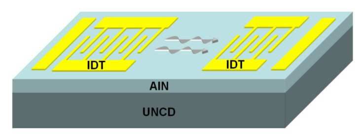
548                                         Acoustic Waves – From Microdevices to Helioseismology

The oscillations of the crystal lattice can than add up by constructive wave interference and
superimpose to a surface wave before being converted back to an electrical signal by further
electrodes.
The passing frequency of a SAW filter can be calculated by

                                                    v0
                                             f0 =                                             (1)
                                                    λ
where represents the wavelength of the acoustic surface wave (corresponding to twice the
distance of the fingers of the IDT) and v0 is the crystal-dependent velocity oft the surface
wave. The operation frequency of a SAW device is closely related to the spacing of the
interdigital transducer (IDT) that is significantly limited by the photolithograph capability
(Springer et al., 1999). Thus one way to achieve higher passing frequencies is to use crystals
with a higher speed of sound, such as sapphire (Caliendo, 2003), SiC (Takagaki, 2002) or
diamond (Yamanouchi et al., 1989)(Nakahata et al., 1992).

3. Diamond as SAW material
The material with the highest speed of sound is diamond with 18000 m/s. Besides the high
speed of sound, diamond features other remarkable properties such as high thermal
conductivity and high hardness to name only a few. Due to its extraordinary properties
natural and HPHT diamond is used for a long time as a material for tools, especially for
grinding or sawing of rocks. Since the 1980s the microcrystalline diamond deposited by thin
film technology is increasingly used. One major problem with the microcrystalline diamond
films deposited in CVD processes – especially for microelectronics and micromechanical
applications with their decreasing structural sizes - is the high surface roughness (Malshe et.
al., 1999). Moreover, high surface roughness results in large propagation loss, reducing the
applicability of the material. Although Sumitomo Electrics developed SAW filters and
resonators with various bandwidth in the 2-5 GHz range it turned out that the polishing of
the rather rough CVD diamond surface was too expensive and time consuming due to the
chemical inertness and highest hardness of diamond and the SAW filters were never
produced in an industrial scale (Fujimori, 1996). Even if one solution to this problem was
demonstrated by using the unpolished nucleation side of freestanding CVD diamond
(Lamara et. al., 2004) this idea never went into production.
Another drawback of the microcrystalline diamond films is that the homogeneous
deposition of such films on substrates with a high aspect ratio is difficult because the films
consist of relatively large crystals.

4. Nanocrystalline diamond as SAW material
The growing interest in nanotechnology and nanostructured materials has encouraged the
research of diamond films with reduced grain size. By reducing the grain size those films
feature rather unique combinations of properties making them potential materials for
emerging technological developments such as Nano/Micro- Electro-mechanical Systems
(N/MEMS) (Auciello et. al., 2004) (Hernandez Guillen, 2004), optical coatings, bioelectronics
(Yang et. al., 2002), tribological applications (Erdemir et. al., 1999) and also surface acoustic
wave (SAW) filters (Bi et. al., 2002).

www.intechopen.com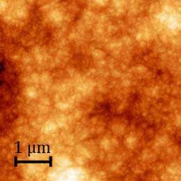
Ultrananocrystalline Diamond as Material for Surface Acoustic Wave Devices            549

The nanostructured films differ from the microcrystalline films in grain size and in
roughness of the surface as shown in Fig. 1.

Fig. 1. Morphological comparison of microcrystalline diamond film (upper picture) and
UNCD film (lower picture). The scale bar in the upper picture corresponds to 1 µm while
the scale bar in the lower picture corresponds to 5 µm
The terms nanocrystalline (NCD) and ultrananocrystalline diamond (UNCD) were coined
by the Argonne National Laboratory group that performed the pioneering work in this field.
These terms were introduced to establish a differentiation to the microcrystalline diamond
films that differ not only in film properties but also in the way they are deposited. The
technology developed at Argonne National Laboratory started from deposition of hydrogen
free plasmas using fullerenes in Ar (Ar/C60) and was thereafter extended to hydrogen
diluted plasmas using Ar/CH4 and gas mixtures containing only about 1 % hydrogen
(either added intentionally or through the thermal decomposition of CH4) (Gruen, 1999).
UNCD is grown from Argon-rich plasma giving it a very fine and uniform structure with
grain sizes between 2 and 15 nm (Auciello et. al., 2004). The grain sizes are independent

www.intechopen.com
550                                       Acoustic Waves – From Microdevices to Helioseismology

from film thickness due to the high secondary nucleation of new growth sites during the
whole deposition that is not taking place in the standard growth of diamond. This can be
shown within the experimental errors when measuring the Young’s modulus (GPa) as a
function of the deposition time (Shen et. al., 2006).
UNCD consists of pure sp3 crystalline grains that can be separated by atomically abrupt (0.5
nm) grain boundaries or embedded in an amorphous 3D matrix. By reducing the grain size
of microcrystalline diamond films the amount of material between the grains is increased.
This matrix in the films can contribute to a large fraction of the overall film, sometimes
exceeding 10 % of the total volume, giving those films a great proportion of non-diamond or
disordered carbon (Auciello et. al., 2004]. But also values down to 5 % sp2-bonded carbon
have been reported and determined by UV Raman spectroscopy and synchrotron based
near-edge X-ray absorption fine structure measurements (NEXAFS) (Gruen, 1998).
In fact the overall volume and structure of the film matrix significantly determine the
properties of nanocrystalline diamond films giving another degree of freedom for the
material. The well-aimed use of an amorphous matrix for nanocrystalline diamond grains
leads to an enormous field of new materials, because a whole class of carbon based materials
(diamondlike carbon, DLC) can be used as matrix that may contain carbon solely (a-C) or
carbon and hydrogen (a-C:H) as well as other components like metals (Me-C:H);
additionally other dopants like silicon, oxygen, halogens or nitrogen may be added with
considerable effect on the film properties. By combining soft matrix properties with the hard
diamond crystals on the nanoscale it is possible to combine hard with elastic properties and
get a material that is hard and tough at the same time. With tailoring the mechanical stress
in the films or the coefficient of thermal expansion it was possible to tailor yet other very
important mechanical properties for the application of UNCD films by adjusting the overall
matrix fraction to the film volume (in the case of a 3D matrix surrounding the nanocrystals)
(Woehrl & Buck, 2007) (Woehrl et. al., 2009).
Thus, when comprehensively characterizing UNCD films, one also has to analyze the matrix
properties. Since the carbon atoms in the matrix have no crystalline configuration and are
indeed amorphous, conventional techniques known from the analysis of amorphous carbon
films can be used.

5. Deposition of UNCD films
It is well accepted that the initial nucleation is one decisive factor for the subsequent CVD
diamond film growth. While a low nucleation density can lead to van-der-Drift growth –
known as the “survival of the largest” – high initial nucleation leads to shorter coalescence
time and lower surface roughness. Due to the fact that substrate pre-treatment can
significantly increase initial nucleation, the pre-treatment is an important process step
already predetermining the film properties (Liu & Dandy, 1995). Three effective seeding
methods are known: Mechanical scratching of the substrate surface (see e.g. (Buck &
Deuerler, 1998)), enhancing the nucleation by applying a bias voltage to the substrate in the
early stages of deposition (Yugo, 1991), and ultrasonically activating the substrate in a
suspension containing diamond powder (Lin et. al., 2006)(Sharma et. al., 2010). Nucleation
densities of 1010 cm-2 or more were achieved with either of these methods. The latter method
was used for the substrates in this work mainly because of the good reproducibility and
uniformity even with larger substrates. Details on the pre-treatment and the deposition
parameters used for the UNCD films deposited in this work are given below.

www.intechopen.com

Ultrananocrystalline Diamond as Material for Surface Acoustic Wave Devices                551

Ultra-Nanocrystalline diamond (UNCD) films were synthesized by microwave plasma
enhanced chemical vapour deposition technique using a 2.45 GHz IPLAS CYRANNUS® I-6”
plasma source. The nanocrystalline films were deposited from an Ar/H2/CH4 plasma.
As standard substrates in this work (100) oriented double side polished silicon wafers with a
thickness of 425 m were used. The substrates were usually cut from a wafer to a size of
about 20 x 20 mm.
To enhance the nucleation of diamond the substrates were ultrasonically scratched for 30
min with a scratching solution consisting of diamond powder (~ 20 nm grain size), Ti
powder (~ 5 nm particle size) and Ethanol in a weight percent ratio of 1:1:100 (wt%).
Afterwards the substrates were ultrasonicated for 15 min in Acetone to clean the surface
from any residues of the scratching solution (Lin et. al., 2006) (Buck, 2008). After the
substrate pre-treatment they were immediately installed into the vacuum chamber placed
on top of the molybdenum substrate holder and the recipient was pumped down to high-
vacuum.
The plasma is ignited at ca. 1 mbar pressure with a process gas mixture of hydrogen (≈ 3 %)
in argon (≈ 97 %) and a MW-power of 1 kW. After the ignition the pressure was slowly
increased up to the deposition pressure (typically 200 mbar) during a 30 min period. This 30
min step is due to two reasons: Firstly the substrate surface is cleaned by the etching effect
of the plasma. Secondly the temperature of the substrate is slowly increased in the process
of the rising pressure. In doing so the substrate is already close to the targeted deposition
temperature before switching to the deposition parameters and introducing the carbon
carrier gas into the chamber. During the whole process of increasing the pressure the MW
power coupling into the plasma is adjusted to the changing conditions. After reaching the
desired deposition pressure the carbon carrier gas was introduced therewith starting the
deposition process.
The nanocrystalline films shown here were deposited at a pressure of 200 mbar from an
Ar/H2/CH4 plasma. To investigate the influence of the hydrogen admixture on the
properties of the deposited films, the percentage of hydrogen in the process gas was varied
between 2 % and 8 % as shown in Table 1.
The MW-power was kept constant at 1 kW and the films were deposited for 5 h.

                      Pressure                    200 mbar
                      Gasflow                     400 sccm
                      H2 fraction                 2%-8%
                      CH4 fraction                0,8 %
                      Ar fraction                 91,2 % - 97,2 %
                      MW-power                    1 kW
                      Deposition time             5h
                      Substrate                   Pretreated Silicon (100)
Table 1. CVD Deposition Parameters

6. Morphology of the films
The deposition parameters were systematically varied to investigate the influence on film
structure and film properties with special attention to the speed of sound and the roughness
of the films as most important properties for the application as SAW filters. Because of that

www.intechopen.com
552 Acoustic Waves – From Microdevices to Helioseismology the main focus was on deposition parameters that influence the diamond grain size and matrix. It is expected that both are directly influencing the elastic modulus of the films and thus the speed of sound. One important parameter that is influencing the crystal size is the admixture of hydrogen in the process gas. The higher the hydrogen fraction the bigger the crystals grow. (Woehrl & Buck, 2007) In previous publications it was suggested that different species for the nucleation on the one hand and the growth of diamond grains on the other hand exist. The ratios of these species determine the macroscopic structure of the growing films by influencing the rate of secondary nucleation and therefore the matrix density and the grain size of the growing crystals. A higher amount of the nucleation species leads to smaller crystals and more material between the grains. A higher amount of growth species allows the grains to grow faster (thus a higher growth rate) suppressing the secondary nucleation. In the literature, C2 was suggested to be the nucleation species (Gruen, 1999) as strong emission of the C2 dimer could be found in the plasmas used for the deposition of fine-grained UNCD films. On the other hand the CH3 radical is generally believed to be the growth species of diamond films (May & Mankelevich, 2008). Without taking part in the discussion concerning specific details of growth and nucleation species, previously published data can be interpreted in a way that these two competitive processes determine the structure of the deposited films. Fig. 2. Morphology of UNCD films deposited with different hydrogen admixtures. The scale bars in all three pictures correspond to 2 µm The atomic force microscope (AFM) is a scanning probe type microscope that offers a resolution of less than a nanometer that is by a factor of 1000 better than the optical www.intechopen.com
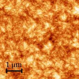
Ultrananocrystalline Diamond as Material for Surface Acoustic Wave Devices                   553

diffraction limit. The AFM consists of a cantilever with a sharp tip with a radius of curvature
in the order of nanometers at its end that is used to scan the sample surface. When the tip is
brought close to the surface, atomic forces between the tip and the sample lead to a
deflection of the cantilever. The deflection of the cantilever is then measured by a laser that
is reflected from the cantilever onto an array of photodiodes. In comparison to the scanning
electron microscope (SEM) that is measuring a two- dimensional image of a sample not
necessarily corresponding to the morphological features, the AFM provides a true three-
dimensional topographical image of the surface giving information about the roughness of
the investigated surface. While specimens measured in SEM needs to be conducting and are
therefore often coated with a thin metal film (e.g. gold) irreversibly alter the film properties,
AFM measurements do not require such special treatments. While the SEM can easily
measure an area in the order of square millimeters with a depth of field on the order of
millimeters the AFM is usually restricted to a maximum scanning area of around 150 m2
with a depth of field in the order of micrometers. Another characteristic that has to be
considered for high resolution AFM is the fact that the quality of an image is limited by the
radius of curvature of the probe tip and can lead to image artifacts. (Sarid, 1991)

Fig. 3. AFM measurements of UNCD samples deposited with 2,5 % H2 (left) and 6 % H2
(right). Both images cover a 5 x 5 µm area
Fig. 2 shows UNCD films deposited with different admixtures of hydrogen to the process
gas. It is clearly seen that the hydrogen is influencing the morphology of the deposited
films. In fact the crystals are larger and the surface is rougher at hydrogen admixtures of 7%
compared to the films deposited at lower admixtures.
Fig. 3 shows an AFM measurement of 5 m thick UNCD films on a Si substrates. The
measured area on the sample was 25 m2. The RMS-roughness (root-mean-squared
roughness) of the surface is measured to be Rq= 21.1 nm for the sample deposited at 2.5 %
H2 (left picture) and Rq= 51.3 nm for the sample deposited at 6 % H2 (right picture).
SEM as well as AFM measurements show that higher hydrogen admixture in the process
gas lead to larger diamond crystals and rougher surfaces.
The RMS-roughness measurements as a function of the hydrogen admixture are shown in
Fig. 4.

www.intechopen.com
554                                       Acoustic Waves – From Microdevices to Helioseismology

Fig. 4. RMS-roughness measurements as a function of hydrogen admixture in process gas

7. Influence of nitrogen admixture on morphology
An especially appealing field of application for UNCD is nitrogen doped semiconducting
films. UNCD films are usually insulating, but n-doping is easily possible by admixture of
nitrogen to the process gas. (Gruen, 2004)
To investigate the influence of the nitrogen admixture in the plasma on the film properties,
more films were deposited at a pressure of 200 mbar with admixtures of nitrogen from 0 %
to 7.5 %.

Fig. 5. High resolution SEM measurement of a UNCD film deposited with 2.5 % hydrogen
and 2.5 % nitrogen admixture. The scale bar shown corresponds to 1 µm

www.intechopen.com
Ultrananocrystalline Diamond as Material for Surface Acoustic Wave Devices                555

High-resolution SEM pictures were taken to investigate the influence of hydrogen and
nitrogen admixture on the morphology of the films. Fig. 5 shows a film deposited with 2.5 %
hydrogen and 2.5 % nitrogen in the plasma. The diamond grains appear to be very fine.
Increasing the nitrogen admixture to 7.5 % and keeping the hydrogen admixture at 2.5 %
changes the shape of the diamond grains. They appear to be needle-shaped as shown in Fig.
6. These measurements show that the nitrogen admixture can influence the shape of the
diamond grains.

Fig. 6. High resolution SEM measurement of a UNCD film deposited with 2.5 % hydrogen
and 7.5 % nitrogen admixture. The scale bar shown corresponds to 200 nm
It is expected that the change in the crystal shape will have a strong influence on the
propagation speed of sound in the material giving yet another degree of freedom when
designing the material for specific applications.

8. SAW pulse technique
The low surface roughness of UNCD films on the one hand and the high speed of sound in
single crystalline diamond on the other hand are making UNCD a very promising material
for SAW application. Yet the decisive question is whether the abundance of grain
boundaries in the films or the amorphous matrix surrounding the grains will change this
picture by e. g. damping the excellent propagation characteristics of surface acoustics waves.
The laser-induced SAW pulse method is capable of measuring the SAW-related (i.e.
mechanical and structural) properties of thin films (Weihnacht et. al, 1997) (Schenk et. al.,
2001) and was used in this work. The applicability of this method for investigating the film
properties of polycrystalline diamond films was demonstrated in previous publications
(Lehmann et. al., 2001). This method allows measuring all necessary material constants and
the wave excitation and propagation parameters decisive for the performance of the SAW
material. The biggest advantage of this method is, that it is not necessary to prepare a
piezoelectric layer or patterning an interdigital transducer (IDT) structure on the surface,
and that rather thin films can also be measured without being disturbed by effects from the
Si substrate. The method is a fast and accurate way to measure acoustic wave propagation

www.intechopen.com
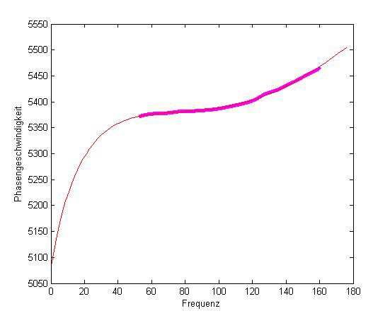
556                                         Acoustic Waves – From Microdevices to Helioseismology

effects in thin film systems (Schneider et. al. 1997). Pioneering work on utilizing surface
acoustic waves as a tool in material science has been done by P. Hess, a general overview
can be found in (Hess, 2002).
A somewhat different setup has been used in this work and is schematically shown in Fig. 7.
This setup is commercially available at Fraunhofer IWS Dresden1.
A pulsed laser beam (N2-laser at 337.1 nm, 0.5 ns pulse duration) is focused on the substrate
by a cylindrical lens to excite a line-shaped broadband SAW pulse via a thermo-elastic
mechanism. A piezoelectric PVDF polymer foil, pressed onto the sample surface by a sharp
steel wedge (width around 5 µm), is used as a broadband sensor for detecting the SAW
pulse propagated along the surface of the thin film system. SAW propagation measurements
are performed for different propagation lengths between a few mm and some cm. The signal
will then be amplified, digitized by an oscilloscope and converted to complex valued spectra
(i.e. amplitude and phase spectra) by a fast Fourier transform algorithm. By doing so for
different well-known propagation lengths on the one hand the SAW phase velocity
dispersion can be determined accurately from the accompanying phase spectra. Knowledge
of the velocity dispersion of a film system is decisive, because it gives the possibility to
recover the materials parameters (e.g. elastic constants, mass density and film thickness). To
derive the elastic properties, a theoretical approach, modeling the films as an isotropic layer
but taking into account the anisotropy of the silicon substrate, was fitted to the measured
dispersion data. The fact that we have a specimen that consists of a film on top of a substrate
introduces a length scale, and thus generates the observed dispersion effect from that the
elastic and mechanical properties can be derived.

Fig. 7. Principle of SAW pulse technique
A measurement of the SAW phase velocity as a function of frequency as well as the fitted
data is shown in Fig. 8. The phase velocity increases with frequency in the case of diamond
on silicon substrate (‘anomalous dispersion’ or ‘stiffening case’), because the smaller
wavelengths, propagating predominantly in the film, have higher phase velocity.

1   LAWave® (http://www.iws.fhg.de/projekte/062/e_pro062.html)

www.intechopen.com
Ultrananocrystalline Diamond as Material for Surface Acoustic Wave Devices               557

Fig. 8. Measured velocity dispersion and fitted data
Beyond that the damping of the amplitude spectra with increasing propagation length can
deliver an estimation of SAW propagation losses due to scattering at thin film imperfections.

Fig. 9. E-modulus as a function of hydrogen admixture
As expected the elastic modulus is higher (the material is stiffer) for higher admixtures of
hydrogen (Fig. 9). This can be explained by the larger diamond crystals and a smaller

www.intechopen.com
558                                      Acoustic Waves – From Microdevices to Helioseismology

contribution of amorphous matrix and the fact that the elastic modulus of the amorphous
matrix is significantly lower than the modulus of the diamond grains. While the elastic
modulus for diamond is around 1220 GPa the elastic modulus of the deposited UNCD films
can reach ca. 65 % of this value.

9. Influence of nitrogen and oxygen on mechanical properties
The influence of the nitrogen admixture on the elastic modulus of the deposited films was
measured by nanoindentation.
The films that were deposited with additional nitrogen are less stiff compared to films
where no additional nitrogen was used. The elastic modulus of the UNCD films deposited
with 2.5 % nitrogen in the plasma was measured to be around 370 GPa and increasing the
nitrogen admixture even higher to 7.5 % in the plasma resulted in UNCD films with values
for the elastic modulus as low as 100 GPa. Thus it was shown that UNCD films deposited
with additional nitrogen are unsuitable for the application as SAW device.
An opposite trend can be found when oxygen is used as admixture to the process gas. It was
shown that the Young’s modulus can be increased up to 950 GPa (ca. 75 % of single
crystalline diamond). The reason can be found in the effective etching of sp2-bonded carbon
by the oxygen in the plasma and thus bigger diamond crystals (Shen et. al., 2006).

10. Feasibility study
As a feasibility study SAW resonators with sputtered AlN film as piezoelectric transducer
have been produced. Fig. 10 shows the concept of the fabricated AlN-UNCD layered SAW
resonator.

Fig. 10. Schematic Structure of AlN-UNCD layered SAW resonator with golden IDT patterns
shaped by photolithography
In the previous chapters it was shown that UNCD films are very suitable as basic material
for SAW applications. It was shown that the addition of hydrogen on the one hand
improves the elastic constants (towards the value of diamond single crystals), and on the
other hand increases the roughness (to values of microcrystalline diamond films), which
leads to large propagation loss. Thus a compromise has to be made. The process parameters
used for this feasibility study are given in table 2.

www.intechopen.com
Ultrananocrystalline Diamond as Material for Surface Acoustic Wave Devices                 559

                      Pressure                    240 mbar
                      Gasflow                     400 sccm
                      H2 fraction                 2%
                      CH4 fraction                 0,8 %
                      Ar fraction                  97,2 %
                      MW-power                    1 kW
Table 2. Deposition conditions
In order to induce a surface acoustic wave in the UNCD material, a piezoelectric layer is
necessary. AlN was chosen for this feasibility study due to being the material with the
highest phase velocity (6700 m/s) among piezoelectric materials (Ishihara et. al., 2002). The
applicability of AlN thin films on various CVD diamond substrates was demonstrated
before (Chalker et. al., 1999).
AlN is an intrinsic piezoelectric material; the wurtzite structure is thermodynamically stable.
Several methods for deposition of AlN-films have been reported e.g. MOCVD (Tsubouchi &
Mikoshiba, 1985), MBE (Weaver et. al., 1990) and reactive DC or RF sputtering (Akiyama et.
al., 1998)(Karmann et. al., 1997). Reactive sputtering processes have the advantage of low
substrate temperatures (Dubois & Muralt, 2001)(Naik et. al., 1999)(Tait & Mirfazli,
2001)(Assouar et. al., 2004). Here, magnetron sputtering processes was chosen, for being a
common and reliable industrial process.
However, highly (002) oriented films with smooth surfaces are required. Thus deposition
parameters (power, pressure, N2 ratio and substrate temperature) have to be systematically
optimized to reach this goal. The influence of oxygen on the film structure was
demonstrated before (Vergara et. al., 2004) showing that a low residual gas pressure is
crucial for the desired film properties. Therefore a vacuum chamber with turbo molecular
pump and a load lock system was used in this work to assure clean conditions. By that,
highly oriented AlN films with very smooth surface were deposited on UNCD films that
turned out to possess good piezoelectric properties. (Lee et. al., 2007). DC power was 300 W
at a pressure of 0.4 Pa and 50 sccm N2 gas flow at 300°C. The film thickness of the AlN films
was ca. 3.5 µm and structure, morphology and bonding structure were characterized by X-
Ray diffractrometry (XRD), scanning electron microscopy (SEM), atomic force microscopy
(AFM), Raman spectroscopy (Renishaw, RA100) and NEXAFS in synchrotron technique.
On top of the AlN film a gold film was deposited by sputtering which was shaped by
conventional photolithography. The resonator consists of a central IDT with reflectors at
each side (Fig. 11).
The produced SAW Resonators were analyzed due to their performance. Thickness of
UNCD as well as AlN have been systematically varied (2 µm to 6.2 µm for UNCD, 1.4 µm to
3.5 µm for AlN). It was measured that with increasing thickness of AlN and UNCD films the
resonance frequency increases as well and the resonance peak become clearer. The increase
of resonance frequency and thus of SAW velocity is due to reduced influence of the low
SAW velocity of the Si substrate. The clearer resonance peak means larger coupling
coefficient, which is due to the relative thickness of AlN piezoelectric layer increasing.
Furthermore the influence of the IDT pair number on the SAW resonator performance was
investigated (100 Pairs to 200 Pairs). It was measured that the resonance frequency and the
resonance strength kept almost the same while doubling the IDT pair numbers.

www.intechopen.com
560 Acoustic Waves – From Microdevices to Helioseismology
This feasibility study indicates that the SAW velocity and coupling coefficient only depend
on the relative thickness of ALN and UNCD films, but are not affected by IDT pattern.
Fig. 11. Schematic Pattern design of SAW Resonator. The actual device consists of significant
more lines
11. Acknowledgment
The authors like to thank Dr. Dieter Schneider at Fraunhofer IWS Dresden for the E-
modulus measurements of the UNCD films and Hanna Bukowska, University Duisburg-
Essen for the AFM measurements.
12. References
Akiyama M., Xu C.-N., Nonaka K., Shobu K., Watanabe T., Thin Solid Films, 315 (1998) 62
Assouar M. B., El Hakiki M., Elmazria O., Alnot P., Tiusan C., Diamond Relat. Mater. 13
(2004) 1111
Auciello O., Birrell J.,. Carlisle J. A, Gerbi J. E., Xiao X., Peng B., Espinosa H. D., J. Phys.:
Condens. Matter 16 (2004) R539
Bi B., Huang W. -S., Asmussen J., Golding B., Diamond Relat. Mater. Vol. 11, Issues 3-6 (2002)
677-680
Buck V., Deuerler F., Diamond Relat. Mater. 7 (1998) 1544
Buck V., J. Opto. Adv. Mater. 10 (2008) 85
Caliendo C., Appl. Phys. Lett. 83 (2003) 4851
Campbell C., Academic Press (1989)
Chalker P. R., Joyce T. B., Johnston C., Crossley J. A. A., Huddlestone J., Whitfield M. D.,
Jackman R. B., Diamond Relat. Mater. 8 (1999) 309
Dubois M.-A., Muralt P., J. Appl. Phys., 89 (2001) 6389
Erdemir A., Fenske G. R., Krauss A. R., Gruen D. M., McCauley T., Csencsits R. T., Surf.
Coat. Techn., 120-121 (1999) 565- 572
www.intechopen.comUltrananocrystalline Diamond as Material for Surface Acoustic Wave Devices 561
Fujimori N., Recent Progresses in Electrical Application of Diamond, 7th European Conference
on Diamond, Diamond-like and Related Materials, 8-13 September 1996
Gruen D. M., MRS Bulletin, Vol. 23, No. 9 (1998) 32
Gruen D. M., Annu. Rev. Mater. Sci. 29 (1999) 211
Gruen D. M., Krauss A. R., Auciello O. H., Carlisle J. A., (2004) US Patent No. 6793849
Hernandez Guillen F. J., Janischowsky K., Ebert W., Kohn E., Phys. Stat. Sol., A, Appl. res.,
vol. 201, no11 (2004) 2553-2557
Hess P., Physics Today, March issue (2002) 42
Ishihara M., Nakamura T., Kokai F., Koga Y., Diamond Relat. Mater. 11 (2002) 408
Karmann S., Schenk H. P. D., Kaiser U., Fissel A., Richter W., Mater. Sci. Eng., B50 (1997) 228
Lamara T., Belmahi M., Elmazria O., Le Brizoual L., Bougdira J., Rémy M., Alnot P., Diamond
Relat. Mater. 13 (2004) 581
Lee Y. C., Lin S. J., Buck V., Kunze R., Schmidt H., Lin C. Y., Fang W. L., Lin I. N., Diamond
Relat. Mater. 17 (2008) 446
Lehmann G., Schreck M., Hou L., Lambers J., Hess P., Diamond Relat. Mater. 10 (2001) 686
Lin I. N., Lee Y. C., Lin S. J., Lin C. Y., Yip M. C., Fang W., Diamond Relat. Mater., Vol 15 No
11-12 (2006) 2046
Liu H., Dandy D. S., Diamond Chemical Vapor Deposition, Nucleation and early growth
stages, Noyes Publications (1995)
Malshe A. P., Park B. S., Brown W. D., Naseem H. A., Diamond Relat. Mater. 8 (1999) 1198
May P. W., Mankelevich Yu. A., J. Phys. Chem. (2008)
Naik R. S., Reif R., Lutsky J. J., Sodini C.G., J. Electrochem. Soc., 146 (1999) 691
Nakahata H., Hachigo A., Shikata S., Fujimori N., IEEE Ultrason. Symp. Proc. (1992) 377
Sarid D., Scanning Force Microscopy, Oxford Series in Optical and Imaging Sciences, Oxford
University Press, New York (1991)
Schenk H. P. D., Feltin E., Vaille M., Gibart P., Kunze R., Schmidt H., M. Weihnacht, E.
Dogheche, Phys. Stat. Sol., A Appl. Res. 188 (2) (2001) 537
Schneider D., Schwarz T., Scheibe H.-J., Panzner M., Thin Solid Films 295 (1997) 107
Shen Z. H., Hess P., Huang J. P., Lin Y. C., Chen K. H., Chen L. C., Lin S. T., J. Appl. Phys., 99
(2006) 124302
Sharma R., Woehrl N., Barhai P. K., Buck V., J. Opt. Adv. Mater., Vol.12 Iss. 9 (2010) 1915
Springer A., Hollerweger F., Weigel R., Berek S., Thomas R., Ruile W., Ruppel C., Guglielmi
M., IEEE Trans. Microwave Theor. Tech. 47 (1999) 2312
Tait R. N., Mirgazli A., J. Vac. Sci. Technol. A, 19 (2001) 1586
Takagaki Y., Santos P.V., Wiebicke E., Brandt O., Schoenherr H.P., Pliig K., Appl. Phys. Lett.
81 (2002) 2538
Tsubouchi K., Mikoshiba N., IEEE Trans. Sonic Ultrason., SU-32 (1985) 634
Vergara L., Clement M., Iborra E., Sanz-Hervás A., García López J., Morilla Y., Sangrador J.,
Respaldiza M. A.
Weaver W., Timoshenko S. P.,. Young D. H, Vibration Problems in Engineering, John Wiley &
Sons., (1990)
Weihnacht M., Franke K., Kaemmer K., Kunze R., Schmidt H., IEEE Ultrason. Symp. Proc.
(1997) 217
Woehrl N., Buck V., Diamond Relat. Mater. 16 (4-7) (2007) 748
Woehrl N., Hirte T., Posth O., Buck V., Diamond Relat. Mater. 18 (2009) 224
Yamanouchi K., Sakurai N., Satoh T., IEEE Ultrason. Symp. Proc (1989) 351
www.intechopen.com562 Acoustic Waves – From Microdevices to Helioseismology Yang W. et al., Nature Materials 1, (2002) 253257 Yugo S., Kanai T., Kimura T., Muto T., Appl. Phys. Lett. 58, (1991) 1036 www.intechopen.com
Acoustic Waves - From Microdevices to Helioseismology
                                      Edited by Prof. Marco G. Beghi

                                      ISBN 978-953-307-572-3
                                      Hard cover, 652 pages
                                      Publisher InTech
                                      Published online 14, November, 2011
                                      Published in print edition November, 2011

The concept of acoustic wave is a pervasive one, which emerges in any type of medium, from solids to
plasmas, at length and time scales ranging from sub-micrometric layers in microdevices to seismic waves in
the Sun's interior. This book presents several aspects of the active research ongoing in this field. Theoretical
efforts are leading to a deeper understanding of phenomena, also in complicated environments like the solar
surface boundary. Acoustic waves are a flexible probe to investigate the properties of very different systems,
from thin inorganic layers to ripening cheese to biological systems. Acoustic waves are also a tool to
manipulate matter, from the delicate evaporation of biomolecules to be analysed, to the phase transitions
induced by intense shock waves. And a whole class of widespread microdevices, including filters and sensors,
is based on the behaviour of acoustic waves propagating in thin layers. The search for better performances is
driving to new materials for these devices, and to more refined tools for their analysis.

How to reference
In order to correctly reference this scholarly work, feel free to copy and paste the following:

Nicolas Woehrl and Volker Buck (2011). Ultrananocrystalline Diamond as Material for Surface Acoustic Wave
Devices, Acoustic Waves - From Microdevices to Helioseismology, Prof. Marco G. Beghi (Ed.), ISBN: 978-953-
307-572-3, InTech, Available from: http://www.intechopen.com/books/acoustic-waves-from-microdevices-to-
helioseismology/ultrananocrystalline-diamond-as-material-for-surface-acoustic-wave-devices

InTech Europe                               InTech China
University Campus STeP Ri                   Unit 405, Office Block, Hotel Equatorial Shanghai
Slavka Krautzeka 83/A                       No.65, Yan An Road (West), Shanghai, 200040, China
51000 Rijeka, Croatia
Phone: +385 (51) 770 447                    Phone: +86-21-62489820
Fax: +385 (51) 686 166                      Fax: +86-21-62489821
www.intechopen.com
You can also read