A Configurable Successive-Cancellation List Polar Decoder Using Split-Tree Architecture
←
→
Page content transcription
If your browser does not render page correctly, please read the page content below
612                                                                                IEEE JOURNAL OF SOLID-STATE CIRCUITS, VOL. 56, NO. 2, FEBRUARY 2021

  A Configurable Successive-Cancellation List Polar
      Decoder Using Split-Tree Architecture
                      Yaoyu Tao , Member, IEEE, Sung-Gun Cho , Graduate Student Member, IEEE,
                                                and Zhengya Zhang , Senior Member, IEEE

   Abstract— Polar codes are capacity-achieving channel codes                     follows a similar schedule as SC decoding; bits are decoded
and they have recently been adopted for fifth-generation (5G)                     sequentially as the decision of one bit depends on the pre-
enhanced mobile broadband (eMBB) control channels. Using                          viously decoded bits. However, unlike in SC decoding where
successive cancellation list (SCL) decoding, the error-correction
performance of polar codes can surpass state-of-the-art codes                     only one decision per bit is kept, SCL keeps a list of L (L > 1)
of a comparable length. However, the sequential SC decoding                       possible bit combinations in the sequential decoding. With
incurs a long latency, and list decoding requires complex tracking                each newly decoded bit, the list of L candidates is updated.
of candidates. We present a split-tree SCL decoder that works                        A larger list size L leads to better accuracy, but the complex-
by dividing a polar code’s decoding tree to sub-trees following                   ity grows exponentially with L and the error-correction per-
a split-tree decoding algorithm. The sub-trees are decoded in
parallel by smaller sub-decoders that reconcile their decisions                   formance tends to saturate after L = 4. A better accuracy can
in every decoding stage. The split-tree list decoder architecture                 also be obtained by adding a cyclic redundancy check (CRC)
improves the throughput and latency proportionally to the split                   to aid the selection of the most likely final decoding decision
factor. By exploiting under-utilized hardware resources, we apply                 from the list of L candidates [3], [4]. With L ≥ 2 and CRC,
frame interleaving to further increase throughput and employ                      the error-correction performance of polar codes with SCL
dynamic clock gating to reduce energy. The results are demon-
strated in a 0.64-mm2 40-nm test chip that implements a split-                    decoding can outperform LDPC codes of a comparable code
4, list-2, eight-frame-interleaved decoding architecture. The chip                length.
supports configurable code lengths up to 1024 bit and variable                       Despite the promise of polar codes with SCL decoding,
code rates. At 0.9 V and room temperature, the chip achieves                      the sequential nature of SCL decoding and the costly tracking
3.25 Gb/s with 42.8-mW power, or 13.2 pJ/b, and demonstrates                      of a list and sorting of candidates lead to low-throughput,
competitive error-correction performance.
                                                                                  high-latency, and high-energy SCL decoding. State-of-the-art
   Index Terms— Dynamic clock gating (CG), frame interleav-                       polar SCL decoders can hardly meet the requirements for
ing, polar codes, split-tree architecture, successive-cancellation                5G; 5G requires multi-Gb/s in throughput and sub-1 µs in
list (SCL) decoder.
                                                                                  latency, and the decoder chip needs to be kept compact and low
                           I. I NTRODUCTION                                       power.

P    OLAR codes, discovered by Arikan [1], have recently
     been adopted by fifth-generation (5G) wireless technol-
ogy standards. They are the first family of codes with an
                                                                                     There are a handful of pre-silicon SCL decoder designs
                                                                                  published in the literature recently. For simplicity and a fair
                                                                                  comparison, we will cite the performance using a common
explicit construction that can provably achieve Shannon’s                         configuration of 1024-bit code length, 1/2 code rate, a list
channel capacity. Using successive-cancellation (SC) decoding                     size of L = 2, and 65-nm CMOS for area. The direct
[1], polar codes achieve the capacity when code length N                          mapping of a log-likelihood ratio (LLR)-based CRC-aided
approaches infinity. However, for moderate-length polar codes                     SCL decoder design [5] was estimated to achieve a 334-Mb/s
of practical interest, SC decoding falls short in terms of                        decoding throughput at an 847-MHz clock frequency. A 4-bit
error-correction performance compared with other advanced                         grouping approach was proposed in [6] to decode neighboring
channel codes, such as low-density parity-check (LDPC)                            bits together for higher throughput, and the decoder design
codes.                                                                            was estimated to achieve 395 Mb/s at 500 MHz. Other
   SC list (SCL) decoding was proposed in [2] to improve the                      speedup techniques, such as partial look-ahead decoder [7] and
error-correction performance of polar codes. SCL decoding                         multi-mode decoder designs [8], were shown in simulation to
                                                                                  achieve 537 Mb/s and 1.21 Gb/s, respectively.
  Manuscript received March 3, 2020; revised May 11, 2020; accepted
June 14, 2020. Date of publication July 20, 2020; date of current version            Area-saving techniques have been developed in [9] and [10].
January 28, 2021. This article was approved by Associate Editor Vivek De.         Hashemi et al. [9] introduced an area-saving strategy based
This work was supported in part by Intel and in part by NSF under Grant           on interpolation-based code construction and layered decoding
CCF-1054270. (Corresponding author: Yaoyu Tao.)
  The authors are with the Department of Electrical Engineering and Com-          scheme, showing up to 50.7% area saving over a conven-
puter Science, University of Michigan, Ann Arbor, MI 48109-2122 USA               tional SCL decoder. Mousavi et al. [10] presented another
(e-mail: taoyaoyu@umich.edu; sunggun@umich.edu; zhengya@umich.edu).               area-saving approach using a partial-sum network that effi-
  Color versions of one or more of the figures in this article are available
online at https://ieeexplore.ieee.org.                                            ciently computes the list candidates, resulting in up to 70%
  Digital Object Identifier 10.1109/JSSC.2020.3005763                             area reduction based on synthesis.
                       0018-9200 © 2020 IEEE. Personal use is permitted, but republication/redistribution requires IEEE permission.
                                     See https://www.ieee.org/publications/rights/index.html for more information.

      Authorized licensed use limited to: University of Michigan Library. Downloaded on March 21,2021 at 16:02:42 UTC from IEEE Xplore. Restrictions apply.
TAO et al.: CONFIGURABLE SCL POLAR DECODER USING SPLIT-TREE ARCHITECTURE                                                                                    613

   Performance-enhanced SCL decoders proposed recently                                                      II. BACKGROUND
include symbol-decision SCL decoder [11] and sphere SCL                            Polar codes exhibit a polarization effect [1] when trans-
decoder designs [12] that were shown in simulation to achieve                   mitted over certain types of channels and decoded using the
398 Mb/s at 500 MHz and 1.23 Gb/s at 1GHz, respectively.                        SC algorithm. The polarization effect refers to that certain
These designs, however, incur a high area overhead.                             bits become highly reliable and the other bits become highly
   Complexity reduction techniques have also been developed,                    unreliable. To use polar codes, information is conveyed over
including simplified SCL (SSCL) and fast-SSCL-SPC [13],                         the reliable bits and the unreliable ones are frozen to prede-
where the SCL tree is pruned and a single parity check (SPC)                    termined values.
is introduced to maintain the error-correction performance.                        An (N, K ) polar code has a code length N and code rate
A fast-SSCL-SPC decoder design was estimated to achieve                         K /N, where N = 2n , n ∈ Z+ . Let u 0N −1 = (u 0 , u 1 , . . . , u N −1 )
1.86 Gb/s at 885 MHz in a 1.048-mm2 area. A follow-                             denotes the vector of input bits to the encoder. The N − K
up rate-flexible fast-SSCL decoder design [14] improved                         least reliable bits in u 0N −1 , called frozen bits, are typically set
the results to an estimated 1.22 Gb/s at 955 MHz in a                           to 0, whereas the remaining K bits, called free bits, are used
1.45-mm2 area. An early stopping criterion was introduced                       to carry information a0K .
[15] to improve the fast-SSCL decoder further to a projected                       An encoder encodes u 0N −1 to the codeword x 0N −1 =
throughput of 2.05 Gb/s at 650 MHz. However, these com-                         (x 0 , x 1 , . . . , x N −1 ). The systematic encoder is mathematically
plexity reduction techniques tend to hurt the error-correction                  described by the following equation:
performance.
   When a high-speed decoder is implemented in silicon,                                   x 0N −1 = u 0N −1 G N = u 0N −1 B N F ⊗n for n ≥ 1                (1)
we can expect that the measured performance to be worse,                        where G N = B N F ⊗n is the N×N generator matrix, B N is
the area to be larger, and the power to be higher than the                      called the bit-reversal permutation matrix, and ⊗n denotes the
estimates, because it is difficult to fully account for all the                 nth Kronecker power
overhead of wiring, clocking, and memory by simulation
                                                                                       ⊗n           ⊗(n−1)          1 0
and synthesis. It is, therefore, more reliable to check silicon                      F =F⊗F                , F=            and F ⊗0 = 1. (2)
measurements to make comparisons. For a simple and fair                                                             1 1
comparison of silicon decoders, we will report the measured                        A polar codeword is produced by first setting the frozen bit
results without applying any process or voltage normalization                   locations to 0. For example, a vector of 4 input bits (N = 4
because popular scaling formulas are no longer reflective of the                and n = 2) is set to u 30 = [0 a0 0 a1 ], where bits 0 and 2 are the
reality of scaling in advanced processes. The latest SC decoder                 frozen bits and are set to 0, and bits 1 and 3 are used to carry
[16] was designed in 180-nm CMOS, occupying 3.17-mm2                            information bits a0 and a1 . For simplicity of understanding,
silicon area. The decoder delivered 655 Mb/s at 382 MHz for                     assume that B4 is identity, and then, the encoder performs the
1024-bit codewords. The first SCL decoder [17] was designed                     following mathematical operation:
in a 28-nm FD-SOI technology, occupying 0.44 mm2 . The                                                                      ⎡              ⎤
decoder achieved 614 Mb/s in throughput, 3.34 µs in latency,                                                                 1 0 0 0
                                                                                                                          ⎢1 1 0 0⎥
and 209 pJ/b in energy at 1.3 V for a 1024-bit code length                             x 03 = u 30 F ⊗2 = 0 a0 0 a1 ⎢       ⎣1 0 1 0⎦
                                                                                                                                           ⎥
and L = 4. The latest SCL decoder [18] was designed in
16-nm FinFET, occupying 2.27 mm2 . The chip demonstrated                                                                     1 1 1 1

a 3.24-Gb/s throughput for 1024-bit codes, but no power                                                 = a0 ⊕ a1 a0 ⊕ a1 a1 a1                  (3)
measurements were reported. Clearly, it is still challenging
                                                                                where modulo-2 operations are used and ⊕ represents
to meet a multi-Gb/s throughput, sub-µs latency, sub-10-pJ/b
                                                                                modulo-2 addition, or XOR. The encoder produces a
energy, and compact silicon area all at the same time.
                                                                                (4, 2) code with a block length of 4 and 2 information bits.
   In this work, we present a 0.64-mm2 configurable SCL
                                                                                   The mathematical operation can be illustrated in the encod-
decoder chip using a split-tree architecture in 40-nm CMOS.
                                                                                ing graph shown in Fig. 1. Note the regular placement of XORs
The decoding tree is split into four subtrees to be decoded
                                                                                between every pair of bits in the first stage and every 2-bit
by four sub-decoders in parallel with decision reconciliation
                                                                                blocks in the second stage. Encoding is done by propagating
in every stage. The new split-tree architecture improves the
                                                                                the bit vector through the graph from left to right.
throughput and cuts the latency by nearly 4×. To maximize
utilization, eight frames are interleaved and decoded simulta-
neously to increase throughput by another 8× to 3.25 Gb/s for                   A. SC Decoding
code length up to 1024 bit and variable code rates. Dynamic                        The bits of the codeword x 03 are modulated and transmitted
clock gating (CG) reduces the peak power dissipation to                         through a physical channel, where noise is injected. On the
42.8 mW at 0.9 V or 13.2 pJ/b. The throughput, energy                           receiver side, each “bit” in the codeword is received as
efficiency, and area efficiency are 5.3×, 15.9×, and 4.0×                       a multibit “soft” value, known as LLRs. A polar decoder
better, respectively, than the SCL decoder chip in a 28-nm                      operates on the LLRs to produce bit estimates. SC is the first
FD-SOI process [17]. Compared with the latest SCL decoder                       and most widely used decoding algorithm for polar codes.
chip [18] in a more advanced 16-nm process, our test chip                          The SC decoding algorithm was proposed in [1]. It can be
achieves a similar throughput and 3× better area efficiency.                    visualized by a decoding trellis, as shown in Fig. 1. The LLRs
These results make this chip suitable for 5G applications.                      are provided on the left-hand side and the bit decisions are

    Authorized licensed use limited to: University of Michigan Library. Downloaded on March 21,2021 at 16:02:42 UTC from IEEE Xplore. Restrictions apply.
614                                                                                IEEE JOURNAL OF SOLID-STATE CIRCUITS, VOL. 56, NO. 2, FEBRUARY 2021

                                                                                  either 0 or 1. The sequential decoding starts from the top and
                                                                                  descends. At each level i , a branch is taken, corresponding to
                                                                                  calculating the likelihood L(û i ), based on which û i is decoded.
                                                                                       For the depth traversal, we can compute the probability of
                                                                                  the path, or the path metric (PM) PM(û i−1 ), for the traversal
                                                                                  to reach a node representing the decision of û i−1 . For the next
                                                                                  step, the path can branch to one of the child nodes, û i = 0 or
                                                                                  û i = 1. The PM can be updated as follows:
                                                                                             PM(û i ) = PM(û i−1 ) + log(1 + e(−1)                         L(û i )
                                                                                                                                                      û i
                                                                                                                                                                        ).   (6)
                                                                                     The goal of SC decoding is to find the most likely path or
                                                                                  the path of the highest PM. To achieve this goal, SC decoding
                                                                                  takes one branch at a level and keeps the path of the highest
                                                                                  PM. The highlighted path on the left in Fig. 2 represents the
                                                                                  survival path in SC decoding. The value associated with each
                                                                                  node is the PM for the decoding path from the root node to that
                                                                                  node. Note that after selecting the survival branch at a level,
                                                                                  the other branch and its child nodes will never be considered.
                                                                                  In the example, the SC decoder chooses the path [0 0 1 1]
                                                                                  with a PM of 0.11.

                                                                                  B. SC List (SCL) Decoding
                                                                                     SC decoding makes one hard decision per step and never
                                                                                  visits other possible paths. Though SC decoding is simple to
                                                                                  implement, it is not guaranteed to find the best global path
Fig. 1. Encoding graph (top) and SC decoding trellis (bottom) of a (4, 2) polar   because the local optimal path may not be part of the global
code.                                                                             optimal path. In the example shown in Fig. 2, the global
                                                                                  optimal path is [1 0 0 1] with a PM of 0.17, but SC decoding
                                                                                  misses this path because it takes the optimal local decision in
made on the right-hand side. The trellis consists of n = log2 N                   step 1.
stages of minimum (F) and summation (G) operations. The F                            The SCL decoding algorithm [2] overcomes this drawback
function receives two LLRs L 1 and L 2 and finds the minimum                      by keeping a list of L candidate paths at each level in
as follows:                                                                       traversing the binary tree. SC decoding can be viewed as a
                                                                                  special case of SCL decoding with L = 1. Fig. 2 shows SCL
      F(L 1 , L 2 ) = sign(L 1 ) · sign(L 2 ) · min(|L 1 |, |L 2 |).       (4)
                                                                                  decoding for L = 2. At each level, the two most likely paths
The G function receives the partial modulo-2 sum of all                           are kept. Moving to the next level, the two most likely paths
previously decoded bits, û s (not annotated in Fig. 1) in addition               branch to four child nodes, leading to four candidate paths.
to the two LLRs, and computes the conditional sum as follows:                     The SCL decoder selects the top two paths among the four to
                                                                                  keep. In the end, the best path is selected.
                G(L 1 , L 2 , û s ) = L 1 · (−1)û s + L 2 .              (5)       In general, an SCL decoder calculates the PMs of all 2L
   The decoding follows a bit-by-bit sequential order.                            child nodes (û i = 0 or û i = 1) that are connected to the
An example of SC decoding is shown in Fig. 1, where in                            L survival paths from the previous step based on (7). The
each decoding step, the highlighted paths and nodes are active.                   decoder selects L paths among the 2L candidates with the
One can easily see that only a subset of F and G functions                        highest PMs to keep. SCL decoding enhances the decoding
at certain stages are active at a time to decode 1 bit, leaving                   accuracy with larger L
                                                                                  PM j (û i ) = PM j (û i−1 ) + log(1 + e(−1)            L(û i )
                                                                                                                                    û i
the other functions in the trellis idle. Assume that it takes                                                                                         )
1 unit time per function (F or G) and the trellis is directly
                                                                                                                      0 ≤ j ≤ L − 1, û i ∈ {0, 1}.                          (7)
mapped in hardware. The latency to decode a bit is variable
ranging from 1 to log2 N. It can be shown that the latency to                        The decoding accuracy can be further improved by concate-
decode an N-bit codeword is 2N − 2. For example, decoding                         nating polar code with CRC [3], [4]. In addition to ranking
a 1024-bit polar code requires 2046 time units. If the trellis                    PMs, codewords corresponding to valid paths also need to pass
is directly mapped to hardware, the hardware complexity is                        CRC check.
approximately O(N log2 N).                                                           An N-bit SCL decoder can be designed with an N-bit SC
   The SC decoding can also be represented by the depth                           decoder core and additional processing logic and memory to
traversal of an N-level binary tree, as shown in Fig. 2. For an                   sort and track L candidate paths. Assume that it takes 1 unit
N = 4 polar code, the binary tree consists of four levels, where                  time to sort and track candidate paths after decoding each
the branching at each level represents the decoding of a bit to                   bit, the SCL decoding latency is (2N − 2) + N. However,

      Authorized licensed use limited to: University of Michigan Library. Downloaded on March 21,2021 at 16:02:42 UTC from IEEE Xplore. Restrictions apply.
TAO et al.: CONFIGURABLE SCL POLAR DECODER USING SPLIT-TREE ARCHITECTURE 615
Fig. 2. SC and SCL (L = 2) decoding represented in a binary tree for a (4, 4) polar code.
Fig. 3. ST-SCL decoding tree for (8, 8) polar code with list size L = 2 and split factor M = 2.
the sorting overhead is only incurred if a bit is a free bit. Take eight-level decoding tree. ST-SCL decoding proceeds level by
the 1024-bit, rate-1/2 polar code selected by the 5G enhanced level. At level i , the decoding consists of two stages.
mobile broadband (eMBB) standard as an example. The code 1) Sub-Decoding: SC sub-decoder 0 and sub-decoder 1
has 512 free bits, so the decoding latency is (2N −2)+ N/2 = operate on their code trellises and compute the likeli-
2558 time units or 25% longer than SC decoding. hood of bit û i and û 4+i , respectively.
2) Reconciliation: The PMs of the four candidate paths
C. Split-Tree SCL (ST-SCL) Decoding per sub-decoder are computed following (7), and the
To reduce the latency and improve the throughput of SCL two survival paths per sub-decoder (called sub-paths)
decoding, an ST-SCL decoding algorithm [19] was proposed. are selected. The sub-paths are assembled, checked for
Conceptually, the N-level decoding tree is split into M sub- constraints, and the top two global paths are selected.
trees of N/M levels, equivalent to splitting the N-bit code The top global paths are then disassembled and distrib-
to M N/M-bit subcodes linked by a constraint matrix. An uted to the two sub-decoders.
ST-SCL decoder consists of M N/M-bit SC sub-decoders Stage 1 is the same as in SCL decoding, but stage 2,
that operate on the subcodes in parallel. Each SC sub-decoder the reconciliation, is new in ST-SCL decoding. If a bit is not a
works on an M× shorter subcode. The hardware complex- frozen bit, the sub-decoder provides L sub-paths. In decoding
ity of all M sub-decoders is O(M · N/M log2 (N/M)) = a level, if none of the M bits are frozen bits, there could
N log2 (N/M). The theoretical decoding latency is reduced by be up to L M possible global paths made by combinations of
a factor of M compared to SC or SCL decoding to O(N/M), sub-paths. The global PMs (GPMs) for the global paths are
and the throughput is increased by the same factor. ST-SCL calculated by summing the sub-path PMs.
decoding requires an extra reconciliation stage to combine sub- The complexity of the reconciliation stage is proportional to
decoders’ local decisions. L M , limiting the maximum split factor and list size. However,
To illustrate ST-SCL decoding, suppose that an N = 8 polar some of the L M global paths are invalid and can be removed
code is decoded with a list size of L = 2 and a split factor of from evaluation. For example, in Fig. 3, if u 5 is a frozen bit,
M = 2. The eight-level decoding tree is split to sub-tree 0 of the paths with û 5 = 1 are not valid because û 5 can only be 0.
four levels and sub-tree 1 of four levels, as shown in Fig. 3, In the best case, if both û i and û 4+i are frozen bits at level i ,
sub-tree 0 for û 30 and sub-tree 1 for û 74 . The decoding of each reconciliation is bypassed. Only in the case when both û i and
subcode is based on a 4-bit code trellis, similar to Fig. 1. û 4+i are free bits at level i , all L M GPMs need to be evaluated.
Frozen bits on each sub-tree are determined by the original Valid global paths are sorted by GPM. The top L global paths
Authorized licensed use limited to: University of Michigan Library. Downloaded on March 21,2021 at 16:02:42 UTC from IEEE Xplore. Restrictions apply.616 IEEE JOURNAL OF SOLID-STATE CIRCUITS, VOL. 56, NO. 2, FEBRUARY 2021
Fig. 5. PE design.
processing element (PE), as shown in Fig. 5. It consists of an
F function described in (4), a G function described in (5) and
XORs to compute partial modulo-2 sums of decoded bits. Back
routing is needed to feed decoded bits back to G functions. The
back routing is implemented by routers between the decoding
Fig. 4. Top-level architecture for a 1024-bit list-2 split-4 configurable SCL
decoder. stages.
A direct mapping of the decoding trellis produces an
eight-stage sub-decoder architecture, and each stage con-
are kept and are disassembled into sub-paths and distributed sists of 128 PEs. However, the hardware utilization of a
to the sub-decoders. direct-mapped architecture is very low. A well-known pattern
in SC decoding is that stage i has at most 2n−1−i PEs active
III. ST-SCL D ECODER A RCHITECTURE FOR H IGH at the same time. For example, in Fig. 1, for an N = 4 bit
T HROUGHPUT AND L OW L ATENCY polar code (n = 2), stage 0 has two PEs active and stage 1 has
one PE active in decoding û 0 . Therefore, instead of the direct
In this section, we present an ST-SCL decoder architecture
mapping, we design the sub-decoder by instantiating only
to realize the near-theoretical latency and throughput improve-
2n−1−i or 27−i PEs in decoding stage i (named Di ), as shown
ments of ST-SCL decoding by an efficient reconciliation stage 7
in Fig. 6. In total, the eight stages contain i=0 2
7−i
=
and a significantly higher utilization of the SC decoding
255 PEs, instead of 128 × 8 = 1024 PEs for a direct-mapped
hardware. A prototype ST-SCL decoder is shown in Fig. 4 for
architecture.
the list size L = 2 and the split factor M = 4. The prototype
To achieve a high clock rate, the sub-decoder is pipelined
design supports configurable code length up to N = 1024
to eight stages, aligned with decoding stages, D0–D7. The
and variable code rates. In decoding a 1024-bit polar code,
pipeline boundaries are shown as dotted lines in Fig. 6. The
the input LLRs are equally split into four groups. A group
255 pipeline registers, L0–L255, store intermediate likelihoods
of 256 LLRs is sent to an SC sub-decoder. The four SC
that are propagated forward, and 255 state registers, U0–U255,
sub-decoders operate on their decoding trellises to compute
store the partial modulo-2 sums of the decoded bits that are
the 4-bit likelihoods in parallel.
routed back.
The reconciliation stage is divided to three steps.
To support a shorter code length, decoding stages can be
1) PM Calculation: For each sub-decoder, the PMs of bypassed. For example, to support a 512-bit code, the code
2L = 4 candidate paths are calculated following (7) and is split into four 128-bit subcodes to be decoded by the
L = 2 sub-paths are selected. four sub-decoders. In each sub-decoder, stage D0 is bypassed
2) Enumeration and Sorting: Based on frozen bit infor- by forwarding the 128 input LLRs to the stage D1 PEs.
mation, valid combinations from the L M = 16 sub- Multiplexers are placed at the inputs to the stage D1 PEs
path combinations are enumerated, and the GPMs are to select either the bypassed input LLRs or the intermediate
calculated. The GPMs are sorted to select the top L = 2 LLRs from the D0 and D1 router. Bypassing stage D0 shortens
global paths. the latency and increases the throughput by reducing the
3) Update: The top global paths are disassembled and pipeline depth from eight to seven stages. The clock inputs
distributed to the four sub-decoders. to the bypassed D0 and D1 pipeline registers are gated to
The three steps are carried out by PM calculator (PMC), global save power. Similarly, to support a 256-bit code, in each sub-
sorter (GS), and data structure updater (DSU) blocks shown decoder, stages D0 and D1 are bypassed by forwarding the
in Fig. 4. We discuss the details of the sub-decoding stage and 64 input LLRs to stage D2 PEs. Both D0 and D1 and D1 and
the reconciliation stage in the following. D2 pipeline registers are clock gated to save power.
A. Sub-Decoder Design B. Reconciliation Design
Each SC sub-decoder decodes a polar code of length up A three-stage reconciliation is done by PMC, GS, and DSU.
to N = 256 bits (n = 8) by recursively passing through For each sub-decoder, the PMC takes the soft decision of a bit
an eight-stage decoder trellis following the sequential order, (LLR of a bit decision being 0) from each sub-decoder output
as shown in Fig. 1. We group an F and a G function in a and the L survival paths to compute the PMs of 2L candidate
Authorized licensed use limited to: University of Michigan Library. Downloaded on March 21,2021 at 16:02:42 UTC from IEEE Xplore. Restrictions apply.TAO et al.: CONFIGURABLE SCL POLAR DECODER USING SPLIT-TREE ARCHITECTURE 617
Fig. 6. 256-bit SCL sub-decoder design.
Fig. 7. Split-tree reconciliation GS architecture for L = 2 and M = 4.
paths by (7). To reduce the complexity of exponentiation and are set to the minimum value. The filtered GPMs undergo a
logarithm evaluations, the PMC employs a piecewise linear four-stage binary sorter to select the top and the second top
approximation in the following equation: global paths. The sub-paths that are present in the top and
⎧ the second top global paths are recorded. Note that the second
⎪
⎨0, for x ≤ −1 top global path is approximated by the smaller GPM of
log(1 + e x ) ≈ 0.5(x + 1), for − 1 < x < 1 (8) the final-stage comparator and this approximation introduces
⎪
⎩
x, for x ≥ 1. negligible performance loss in mid-to-high SNR regime.
Finally, the DSU disassembles the top L global paths to
The PMC consists of four sets of hardware, one set per sub-
constitute sub-paths and distributes them to the sub-decoders.
decoder. A set consists of one negation block to compute the
The disassembling is done by marking the corresponding local
LLR of a bit decision being 1, two log-approximation blocks,
PMs as visited and updating the list state registers in controller.
and four adders to compute the PMs of four candidate paths.
The back-propagation XORs also updates the state registers Us
From the four candidate paths, the top two candidate paths are
in sub-decoders. The worst case DSU delay happens when the
selected to be passed on to the GS.
newly decoded bits back-propagate through all eight stages of
The GS is shown in Fig. 7. It consists of a feasible path
XOR network inside sub-decoders.
calculator, a global path calculator, and a binary sorter. The
The three-step reconciliation, including PMC, GS, and
feasible path calculator uses frozen bit lookup tables (LUTs)
DSU, occupies only 0.02 mm2 in 40-nm CMOS when syn-
to generate control signals for selecting only the valid global
thesized at a 500-MHz clock frequency.
paths. The LUTs can be reconfigured to support different code
lengths and rates. To save area, the LUTs are implemented as
four copies of length-256 cyclic shift registers to store frozen C. Pipeline and Hardware Utilization
bit indicators for each subcode of up to 256 bits. In the ST-SCL decoder, the four sub-decoders operate
The global path calculator sums up all combinations of in parallel and feed to the three-step reconciliation. The
sub-paths using L M four-input adders. For M = 4 and L = 2, sub-decoder is pipelined to eight stages, from D0 to D7; and
there are a total of L M = 16 possible global paths. The the three-step reconciliation is pipelined to three stages, PMC,
complexity of wiring to route the local PMs and the number GS, and DSU, abbreviated by P, S, and U , respectively. What
of adders increase exponentially with the split factor M, complicates the design is that the decoding of any given bit
limiting the practical M to 4. The 16 GPMs are filtered by follows a different set of pipeline stages. The irregularity is
the feasible path calculator. The GPMs of the invalid paths due to two factors: 1) the variable path through the trellis for
Authorized licensed use limited to: University of Michigan Library. Downloaded on March 21,2021 at 16:02:42 UTC from IEEE Xplore. Restrictions apply.618 IEEE JOURNAL OF SOLID-STATE CIRCUITS, VOL. 56, NO. 2, FEBRUARY 2021
Fig. 8. ST-SCL decoding pipeline for a single frame (top) and eight-frame interleaving (bottom).
decoding a bit, as shown in Fig. 1, and 2) S and U stages can to one stage of 128 PEs. Folding reduces the PE count to
be bypassed if all four bits at a given level are frozen bits. approximately half, allowing the PE utilization to be doubled
An example is shown in Fig. 8. Decoding the 4 bits in to 3.14%, which is still low. Complex wiring, muxes, and
level 0 by the four sub-decoders requires going through all control logic have to be added to support PE reuse, costing an
eight stages of the trellis, corresponding to D0–D7 pipeline estimated 24% extra area and 21% longer clock period based
stages; decoding the 4 bits in level 1 by the four sub-decoders on synthesis.
requires only the last two stages of the trellis, corresponding A better approach is to exploit the pipeline to accommodate
to D6 and D7 pipeline stages; and so on. In decoding level 0, decoding of multiple frames at the same time. Through frame
all four bits are frozen bits, so S and U pipeline stages are interleaving, the same hardware is used to process more
bypassed; similarly, in decoding levels 1–3, S and U stages workload, improving the hardware utilization and increas-
are also bypassed. The irregularity is handled by routers in the ing the throughput proportional to the number of frames.
sub-decoders and the bypass switches in reconciliation. However, resource contentions may occur. Suppose that eight
To estimate latency and throughput, we use the 1024-bit, frames are launched over eight consecutive cycles (interleave
rate-1/2 polar code selected by the 5G eMBB standard as gap = 1), as shown in the eight-frame-interleaved pipeline
an example. The code has 512 frozen bits. We split the chart in Fig. 8. The highlighted parts show contentions for
code into M = 4 subcodes to be decoded by four 256-bit a hardware unit. Resolving the contentions requires multiple
sub-decoders in parallel. Since the latency of SC decoding is copies of hardware units, including PMCs, GSs, and DSUs.
2N −2 for an N-bit code, decoding a 256-bit subcode requires For example, two copies of D6 and four copies of D7 are
510 clock cycles. The reconciliation latency depends on the required in each sub-decoder, and four copies of PMCs and
frozen bit pattern. Among 256 decoding levels, 101 levels two copies of GSs and DSUs are required in reconciliation.
involve four bits that are all frozen bits and the S and U We studied the optimal number of frames for interleaving
stages are bypassed, and the remaining 155 levels involve by first checking the amount of hardware addition, as shown
at least one free bit. Therefore, the reconciliation latency is in Fig. 9. With more frames, more hardware units are needed
101 + 155 × 3 = 566 clock cycles. In total, ST-SCL decoding for the worst case resource contention scenarios. However,
requires 510 + 566 = 1076 cycles to decode a 1024-bit code due to the general low utilization of the baseline architecture,
or 47% times faster than SC decoding. resource contentions due to frame interleaving are relatively
The hardware utilization is low if one frame is processed infrequent. As a result, only a small number of hardware units
at a time. During sub-decoding, P, S, and U stages are idle, need to be added to the baseline architecture, making frame
and during reconciliation, D0–D7 stages are idle. Furthermore, interleaving a relatively low-cost approach to increasing both
during sub-decoding, only one of D0–D7 stages is active at throughput and efficiency. For example, to support eight-frame
a time. If we define utilization as the average fraction of interleaving, only five additional PEs are needed on top of the
active hardware units at a given clock cycle, sub-decoders’ 255 PEs in each sub-decoder, and four copies of PMCs and
PE utilization is only 1.57%, PMC’s utilization is 23.8%, and two copies of GSs and DSUs are needed for reconciliation.
GS and DSU utilization are 14.4%. There is ample room to What is not shown in Fig. 9 is that N-frame interleaving also
increase the utilization for improving the efficiency and the requires N copies of state registers in each sub-decoder as
throughput of the hardware. well as muxes to select frames.
Besides hardware duplication, frame interleaving also
requires extra control and dispatchers, which become more
IV. F RAME I NTERLEAVING TO E NHANCE
expensive with more frames. Interleaving more frames pro-
T HROUGHPUT AND E FFICIENCY
duces a higher throughput, but the silicon area increases too.
To increase the sub-decoders’ PE utilization, a straightfor- We use chip synthesis in a 40-nm CMOS technology at room
ward way is to fold the eight stages of 255 PEs in Fig. 6 temperature and the nominal voltage 0.9 V to evaluate the
Authorized licensed use limited to: University of Michigan Library. Downloaded on March 21,2021 at 16:02:42 UTC from IEEE Xplore. Restrictions apply.TAO et al.: CONFIGURABLE SCL POLAR DECODER USING SPLIT-TREE ARCHITECTURE 619
Fig. 9. Allocation of additional hardware units to support N -frame interleaving.
Fig. 12. (a) Power breakdown of a split-4, list-2, eight-frame-interleaved
ST-SCL decoder. (b) Detailed breakdown of the sequential switching power
Fig. 10. Throughput and area of frame-interleaved designs. Silicon area is of the ST-SCL decoder. Power is obtained from chip synthesis in 40-nm
obtained from chip synthesis in 40-nm CMOS at room temperature and the CMOS at room temperature and the nominal 0.9-V supply voltage.
nominal 0.9-V supply voltage.
Fig. 13. Chip design optimization summary based on chip synthesis in 40-nm
CMOS at room temperature and the nominal 0.9-V supply voltage.
Fig. 11. Improved hardware utilization with frame interleaving.
list-2 eight-frame-interleaved ST-SCL decoder was synthe-
area with a different number of interleaved frames. As shown sized and placed and routed in a 40-nm CMOS process.
in Fig. 10, the increased throughput initially outpaces the Fig. 12(a) shows the power breakdown of the decoder. The
increase in silicon area until it reaches eight frames. If we use switching power of the sequential circuits is the dominant
area efficiency, i.e., throughput/area, as the metric, eight-frame portion, claiming 88% of the total power. Further breakdown
interleaving is optimal, as it increases the throughput by 7.8× of the switching power of sequential circuits in Fig. 12(b)
and the area by only three times over the baseline architecture. shows that the switching power of the sub-decoders, the PMCs,
As shown in Fig. 11, with eight-frame interleaving, two and the sorters account for more than 90% of the sequential
copies of D6 and four copies of D7 are used in each sub- switching power.
decoder, and the PE utilization increases by 7.8×, from 1.57%
to 12.4%. Four copies of PMCs, two copies of GSs and V. S UMMARY OF D ECODER D ESIGN O PTIMIZATION S TEPS
DSUs are also needed, with a utilization of 47.3%, 57.3%, We summarize the decoder design optimization steps based
and 57.3%, respectively, which are 2×, 4×, and 4× higher on 40-nm CMOS synthesis for the code length of 1024 bit and
than the baseline. a list size of 2 in Fig. 13 and Table I. The conventional SCL
Frame interleaving proportionally increases the number of decoder is set as the baseline. The baseline runs at the maxi-
state registers. To estimate the power consumption, the split-4, mum clock rate of 720 MHz to achieve a 240-Mb/s throughput
Authorized licensed use limited to: University of Michigan Library. Downloaded on March 21,2021 at 16:02:42 UTC from IEEE Xplore. Restrictions apply.620 IEEE JOURNAL OF SOLID-STATE CIRCUITS, VOL. 56, NO. 2, FEBRUARY 2021
TABLE I
C HIP D ESIGN O PTIMIZATION S UMMARY BASED ON C HIP S YNTHESIS IN 40-nm CMOS AT ROOM
T EMPERATURE AND THE N OMINAL 0.9-V S UPPLY V OLTAGE
Fig. 14. CG design for split-4, eight-frame-interleaved ST-SCL polar decoder.
and a 0.43-ms latency with a core area of 0.138 mm2 . The PE outputs clock enable signals by reading from the LUTs. In the
utilization is only 0.49%. test chip design, we disable clock input to a sub-decoder stage
The split-4 ST-SCL decoder enhances the throughput and if the stage will be idle for at least three consecutive cycles to
latency by 2.3× to 547 Mb/s and 0.19 ms, respectively, while avoid frequent off/on switching. For the shorter code lengths
incurring a 30% area penalty. Compared with the baseline, of 512 and 256 bit, CG latch 0 and latch 1 inside sub-decoders
the ST-SCL decoder increases the PE utilization to 1.57% and will switch off the clock inputs to the bypassed stages. The
the area efficiency to 3.11 Gb/s/mm2 . Folding the ST-SCL CG controller also stores the number of required PMCs and
decoder produces 1.9× higher throughput and lower latency GSs for each cycle and disables the clock inputs to unused
compared with the baseline. Folding also increases the PE PMCs and GSs to save power.
utilization to 3.14%.
The split-4 ST-SCL decoder with eight-frame-interleaving VI. D ECODER C HIP I MPLEMENTATION AND
boosts the throughput by 17.8× to 4.27 Gb/s and shortens M EASUREMENT R ESULTS
the latency by 2.3× compared with the baseline. The area A test chip for the split-4, list-2, eight-frame-interleaved,
efficiency is 4.57× better than the baseline. The PE utilization configurable polar ST-SCL decoder supporting code length
is increased to 12.4%. up to 1024 bit and variable code rates was implemented in
We apply a per-block CG strategy to reduce the active 40-nm CMOS. The chip microphotograph is shown in Fig. 15.
power consumption of sequential circuits by exploiting the The chip measures 0.91 mm × 0.91 mm, and the decoder
idle cycles. The PE utilization of the sub-decoders is 12.4%, core measures 0.70 mm × 0.91 mm or 0.64 mm2 . The
and the utilization of the reconciliation stage is approximately chip incorporates input buffers to provide input vectors and
50%. By systematically gating the clocks to unused hardware output buffers to collect the decoded bits. An on-chip CPU
units, the active power is reduced proportionally. with UART interface enables testing of various code lengths,
Adding per-block CG increases the area by 2.6% for the code rates, number of interleaving frames, and CG. It also
eight-frame-interleaved split-4 ST-SCL decoder. CG is imple- supports optional post-processing. The chip is verified to be
mented with a CG controller sending clock enables to sub- fully functional for the code lengths of 512 and 1024 bit and
decoders, PMCs, and GSs, as shown in Fig. 14. Clock enable the code rates of 1/2, 2/3, 3/4, and 5/6.
patterns are determined by code configurations, including
code length, code rate, and frozen bit locations. For each
code, clock enable patterns are pre-computed based on stages A. Measurement Results
D0–D7 active/idle patterns, and they are stored in LUTs inside The bit error rate (BER) and frame error rate (FER) for
the CG controller. The decoder top controller sends the code decoding a split-4, list-2, 1024-bit rate-1/2 code are plotted
configuration to the CG controller, and the CG controller in Fig. 16. The 6-bit quantized decoder uses an 8-bit CRC
Authorized licensed use limited to: University of Michigan Library. Downloaded on March 21,2021 at 16:02:42 UTC from IEEE Xplore. Restrictions apply.TAO et al.: CONFIGURABLE SCL POLAR DECODER USING SPLIT-TREE ARCHITECTURE 621
Fig. 17. Measured throughput, power, and energy efficiency of various
configurations for the 40-nm ST-SCL decoder chip in decoding 1024-bit rate-
1/2 polar codes at room temperature.
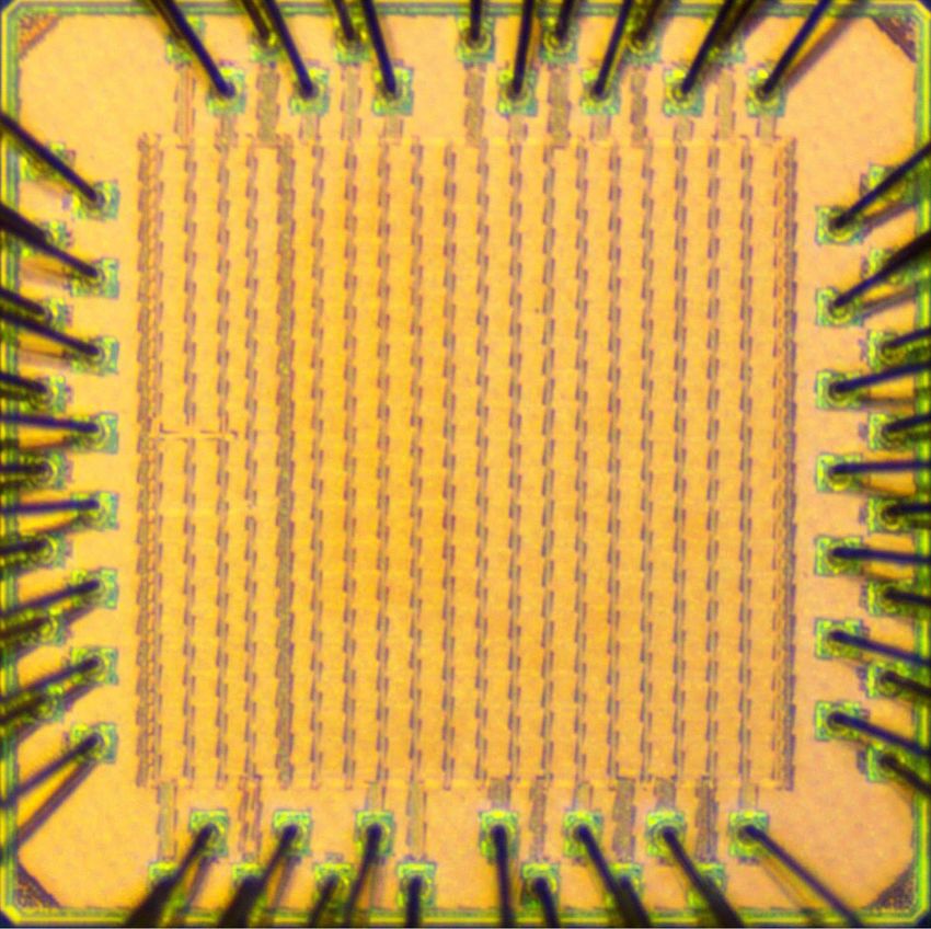
Fig. 15. Microphotograph of the decoder test chip fabricated in a 40-nm
CMOS technology.
Fig. 18. Measured power of the 40-nm test chip for decoding 512- and
1024-bit polar codes at room temperature and different supply voltages.
Fig. 16. BER and FER performance of 1024-bit rate-1/2 ST-SCL decoder eight-frame-interleaved design is mainly attributed to three
with split factor 4 and list size 2 using 6-bit quantization and 8-bit CRC. factors: 1) the number of state registers (Ls and Us) in the
sub-decoders is increased by 8×; 2) PE, PMC, and GS/DSU
utilization are increased to 12.4%, 47.3%, and 57.3%, respec-
to assist with final path selection for a better error-correction tively; and 3) decoder controller and router switching activities
performance. The design achieves an FER of 10−5 at 3.55 dB, are increased to support decoding eight frames in parallel.
demonstrating 0.15- and 0.65-dB coding gains over the Among the three factors, factor 1) contributes the most power
floating-point SCL (L = 2) decoder and the floating-point SC increase. The sub-decoders are estimated to consume 31% of
decoder, respectively. Compared with the floating-point belief the total power, 90% of which is sequential power consumed
propagation (BP) decoder, our design provides a 1.1-dB coding by state registers. Compared with a decoder that supports
gain. only one frame at a time, the eight-frame-interleaved design
The decoder test chip runs at a maximum clock frequency requires eight sets of state registers, and the total chip power
of 430 MHz at a 0.9-V nominal supply voltage and room increases by about 2.2× (calculated from 31% × 90% ×8) due
temperature when decoding 1024-bit, rate-1/2 polar codes. to the sub-decoder’s state register increase. Combining factors
Fig. 17 summarizes the measured throughput and power 2) and 3), the power of the eight-frame interleaved decoder
consumption of the test chip. In the baseline design without increases by 2.5× over the single-frame decoder.
frame interleaving and CG, the decoder delivers a 407-Mb/s CG can be enabled to reduce the power consumption to
throughput. It consumes 25.39-mW power, which translates 42.80 mW and improve the energy efficiency to 13.17 pJ/b.
to an energy efficiency of 61.92 pJ/b. To achieve a higher Scaling the supply voltage from 0.9 to 0.6 V reduces the
throughput, eight-frame interleaving is enabled to provide maximum clock frequency from 430 to 100 MHz and further
an 8× throughput to 3.25 Gb/s at a power consumption improves the energy efficiency to 7.40 pJ/b.
of 64.29 mW. The energy efficiency is improved to 19.80 pJ/b, Fig. 18 shows the power consumption for decoding
due to the efficient sharing and reusing of under-utilized 1024- and 512-bit codes of rate 1/2 and 3/4, and the effect
hardware. The power increase from the baseline to the of frame interleaving and CG. The power was recorded at
Authorized licensed use limited to: University of Michigan Library. Downloaded on March 21,2021 at 16:02:42 UTC from IEEE Xplore. Restrictions apply.622 IEEE JOURNAL OF SOLID-STATE CIRCUITS, VOL. 56, NO. 2, FEBRUARY 2021
TABLE II
C OMPARISON OF S TATE - OF - THE -A RT P OLAR D ECODERS
the lowest operating voltage at each frequency. From the technology nodes, our design exceeds the throughput reported
baseline without frame interleaving to eight-frame interleav- in [17] and [18]. After technology normalization, our design
ing, the power increases as expected, but the per-block CG achieves an order of magnitude better area efficiency (in
effectively lowers the power. For a given code length, decoding Gb/s/mm2 ) and an order of magnitude better energy efficiency
a higher code rate (in this case 3/4) consumes slightly higher (in pJ/b) than [17] and [18] (note that [18] did not report
power, due to more switching activities to process more free power, and the energy efficiency cannot be estimated).
bits. For a given code rate, decoding a shorter code length Compared with the much simpler SC decoder designs [16],
costs less power, due to the sub-decoders’ bypassing of trellis [22], the ST-SCL decoder delivers a better error-correction
stages. performance as shown in Fig. 16, and the energy efficiency
is more than an order of magnitude better after technology
normalization. Compared with the most recent BP decoder
B. Comparisons synthesis [23], the ST-SCL decoder achieves more significant
The ST-SCL decoder test chip is compared with the state-of- coding gain as shown in Fig. 16, and the energy efficiency is
the-art polar decoder designs in Table II, including both syn- still 4.2× better.
thesis results (where no test chip was fabricated and power was
not reported) and silicon measurements. Compared with the
VII. C ONCLUSION
most recent synthesis results of SCL decoders [20], [21], our
ST-SCL chip outperforms by more than 2.15× in throughput We present a fabricated test chip in a 40-nm CMOS tech-
and 1.88× in area efficiency than [20] before normalization. nology that implements an ST-SCL decoder for polar codes.
After technology normalization to 40-nm and 0.9-V supply In this design, a given polar code is split into four sub-codes
voltage, the area efficiency of [20] and [21] surpass our design, and decoded separately with smaller sub-decoders followed
which is mainly due to three factors: 1) [20] and [21] do not by a reconciliation step in every decoding stage. Taking
support variable code lengths and rates; 2) [20] and [21] use advantage of the under-utilized PEs in the sub-decoders, eight
SSCL or modified SCL decoding algorithms with performance frames are interleaved and decoded in parallel to achieve a
loss; and 3) [20] and [21] are synthesis results only without high throughput and area efficiency. The decoder supports
silicon measurements. Only silicon results capture the layout variable code lengths up to 1024 bit and variable code rates by
and wiring congestion overheads that can be significant in programming the control LUTs. Per-block CG is implemented
high-throughput decoder designs. to further reduce the power consumption and improve energy
Compared with the recent fabricated silicon SCL polar efficiency. The 0.64-mm2 test chip is measured to achieve
decoders [17], [18] in more advanced 28- and 16-nm a decoding throughput of 3.25 Gb/s at 430 MHz at the
Authorized licensed use limited to: University of Michigan Library. Downloaded on March 21,2021 at 16:02:42 UTC from IEEE Xplore. Restrictions apply.TAO et al.: CONFIGURABLE SCL POLAR DECODER USING SPLIT-TREE ARCHITECTURE 623
nominal supply voltage of 0.9 V, consuming 13.17 pJ/b, and [20] F. Ercan, T. Tonnellier, and W. J. Gross, “Energy-efficient hardware
it demonstrates a competitive error-correction performance. architectures for fast polar decoders,” IEEE Trans. Circuits Syst. I, Reg.
Papers, vol. 67, no. 1, pp. 322–335, Jan. 2020.
Voltage and frequency scaling of the chip to 0.6 V and [21] W. Song et al., “Efficient successive cancellation stack decoder for polar
100 MHz further improves the energy efficiency to 7.4 pJ/b at codes,” IEEE Trans. Very Large Scale Integr. (VLSI) Syst., vol. 27, no. 11,
a reduced throughput of 760 Mb/s. The test chip outperforms pp. 2608–2619, Nov. 2019.
[22] R. Shrestha and A. Sahoo, “High-speed and hardware-efficient suc-
the state-of-the-art SCL polar decoder chips in throughput, cessive cancellation polar-decoder,” IEEE Trans. Circuits Syst. II, Exp.
and its normalized energy efficiency and area efficiency are Briefs, vol. 66, no. 7, pp. 1144–1148, Jul. 2019.
an order of magnitude better than the latest published work. [23] Y.-T. Chen, W.-C. Sun, C.-C. Cheng, T.-L. Tsai, Y.-L. Ueng, and
C.-H. Yang, “An integrated message-passing detector and decoder for
polar-coded massive MU-MIMO systems,” IEEE Trans. Circuits Syst. I,
ACKNOWLEDGMENT Reg. Papers, vol. 66, no. 3, pp. 1205–1218, Mar. 2019.
[24] H.-Y. Yoon and T.-H. Kim, “Efficient successive-cancellation polar
The authors would like to thank Dr. Farhana Sheikh and decoder based on redundant LLR representation,” IEEE Trans. Circuits
collaborators at Intel Labs for advice. Syst. II, Exp. Briefs, vol. 65, no. 12, pp. 1944–1948, Dec. 2018.
R EFERENCES
[1] E. Arikan, “Channel polarization: A method for constructing capacity- Yaoyu Tao (Member, IEEE) is currently pursuing
achieving codes for symmetric binary-input memoryless channels,” IEEE the Ph.D. degree with the University of Michigan,
Trans. Inf. Theory, vol. 55, no. 7, pp. 3051–3073, Jul. 2009. Ann Arbor, MI, USA.
[2] I. Tal and A. Vardy, “List decoding of polar codes,” in Proc. IEEE Int. He is also with the Wireless Research and Devel-
Symp. Inf. Theory Proc., Jul. 2011, pp. 1–5. opment Team, Qualcomm, as a Staff Engineer,
[3] K. Niu and K. Chen, “CRC-aided decoding of polar codes,” IEEE where he was promoted from Senior Engineer
Commun. Lett., vol. 16, no. 10, pp. 1668–1671, Oct. 2012. to Staff Engineer in October 2019. His research
[4] B. Li, H. Shen, and D. Tse, “An adaptive successive cancellation list interests expand to VLSI circuits, architecture and
decoder for polar codes with cyclic redundancy check,” IEEE Commun. systems for computing, communications, signal
Lett., vol. 16, no. 12, pp. 2044–2047, Dec. 2012. processing, and machine learning applications.
[5] A. Balatsoukas-Stimming, M. Bastani Parizi, and A. Burg, “LLR-based
successive cancellation list decoding of polar codes,” IEEE Trans. Signal
Process., vol. 63, no. 19, pp. 5165–5179, Oct. 2015.
[6] B. Yuan and K. K. Parhi, “Low-latency successive-cancellation list
decoders for polar codes with multibit decision,” IEEE Trans. Very Large
Sung-Gun Cho (Graduate Student Member, IEEE)
Scale Integr. (VLSI) Syst., vol. 23, no. 10, pp. 2268–2280, Oct. 2015.
received the B.S. and M.S. degrees in electrical
[7] J. Lin, C. Xiong, and Z. Yan, “A high throughput list decoder architecture
engineering from the Korea Advanced Institute of
for polar codes,” IEEE Trans. Very Large Scale Integr. (VLSI) Syst.,
Science and Technology (KAIST), Daejeon, South
vol. 24, no. 6, pp. 2378–2391, Jun. 2016.
Korea, in 2010 and 2012, respectively. He is cur-
[8] C. Xiong, J. Lin, and Z. Yan, “A multimode area-efficient SCL polar
rently pursuing the Ph.D. degree in electrical and
decoder,” IEEE Trans. Very Large Scale Integr. (VLSI) Syst., vol. 24,
computer engineering with the University of Michi-
no. 12, pp. 3499–3512, Dec. 2016.
gan, Ann Arbor, MI, USA.
[9] S. A. Hashemi, M. Mondelli, S. H. Hassani, C. Condo, R. L. Urbanke,
From 2012 to 2015, he was with SK Hynix
and W. J. Gross, “Decoder partitioning: Towards practical list decoding
Inc., Icheon, South Korea, where he was involved
of polar codes,” IEEE Trans. Commun., vol. 66, no. 9, pp. 3749–3759,
in system-on-chip (SoC) design and implementa-
Sep. 2018.
tion of error control coding. His research interests include energy-efficient,
[10] M. Mousavi, Y. Fan, C.-Y. Tsui, J. Jin, B. Li, and H. Shen, “Effi-
high-performance architecture, VLSI circuits and systems for neuromorphic
cient partial-sum network architectures for list successive-cancellation computing, error control coding, and machine learning applications.
decoding of polar codes,” IEEE Trans. Signal Process., vol. 66, no. 14,
pp. 3848–3858, Jul. 2018.
[11] C. Xiong, J. Lin, and Z. Yan, “Symbol-decision successive cancellation
list decoder for polar codes,” IEEE Trans. Signal Process., vol. 64, no. 3,
pp. 675–687, Feb. 2016. Zhengya Zhang (Senior Member, IEEE) received
[12] S. A. Hashemi, C. Condo, and W. J. Gross, “A fast polar code list the B.A.Sc. degree in computer engineering from
decoder architecture based on sphere decoding,” IEEE Trans. Circuits the University of Waterloo, Waterloo, ON, Canada,
Syst. I, Reg. Papers, vol. 63, no. 12, pp. 2368–2380, Dec. 2016. in 2003, and the M.S. and Ph.D. degrees in elec-
[13] S. A. Hashemi, C. Condo, and W. J. Gross, “Fast and flexible successive- trical engineering from the University of California
cancellation list decoders for polar codes,” IEEE Trans. Signal Process., at Berkeley (UC Berkeley), Berkeley, CA, USA,
vol. 65, no. 21, pp. 5756–5769, Nov. 2017. in 2005 and 2009, respectively.
[14] S. A. Hashemi, C. Condo, M. Mondelli, and W. J. Gross, “Rate-flexible He has been a Faculty Member with the University
fast polar decoders,” IEEE Trans. Signal Process., vol. 67, no. 22, of Michigan, Ann Arbor, MI, USA, since 2009,
pp. 5689–5701, Nov. 2019. where he is currently an Associate Professor with the
[15] D. Kim and I.-C. Park, “A fast successive cancellation list decoder Department of Electrical Engineering and Computer
for polar codes with an early stopping criterion,” IEEE Trans. Signal Science. His research interest includes low-power and high-performance VLSI
Process., vol. 66, no. 18, pp. 4971–4979, Sep. 2018. circuits and systems for computing, communications, and signal processing.
[16] H.-Y. Yoon, S.-J. Hwang, and T.-H. Kim, “A 655 Mbps successive- Dr. Zhang was a recipient of the David J. Sakrison Memorial Prize from
cancellation decoder for a 1024-bit polar code in 180 nm CMOS,” UC Berkeley in 2009, the National Science Foundation CAREER Award
in Proc. IEEE Asian Solid-State Circuits Conf. (A-SSCC), Nov. 2018, in 2011, the Intel Early Career Faculty Award in 2013, and the University of
pp. 281–284. Michigan College of Engineering Neil Van Eenam Memorial Award in 2019.
[17] P. Giard et al., “PolarBear: A 28-nm FD-SOI ASIC for decoding of He has been an Associate Editor of the IEEE T RANSACTIONS ON V ERY
polar codes,” IEEE J. Emerg. Sel. Topics Circuits Syst., vol. 7, no. 4, L ARGE S CALE I NTEGRATION S YSTEMS since 2015. He has been serving
pp. 616–629, Dec. 2017. on the Technical Program Committees of the Symposium on VLSI Circuits
[18] X. Liu et al., “A 5.16Gbps decoder ASIC for polar code in and the IEEE Custom Integrated Circuits Conference (CICC) since 2018.
16nm FinFET,” 2018, arXiv:1807.01451. [Online]. Available: http:// He was an Associate Editor of the IEEE T RANSACTIONS ON C IRCUITS AND
arxiv.org/abs/1807.01451 S YSTEMS —PART I: R EGULAR PAPERS from 2013 to 2015 and the IEEE
[19] B. Li, H. Shen, and D. Tse, “Parallel decoders of polar codes,” 2013, T RANSACTIONS ON C IRCUITS AND S YSTEMS —PART II: E XPRESS B RIEFS
arXiv:1309.1026. [Online]. Available: http://arxiv.org/abs/1309.1026 from 2014 to 2015.
Authorized licensed use limited to: University of Michigan Library. Downloaded on March 21,2021 at 16:02:42 UTC from IEEE Xplore. Restrictions apply.You can also read