Bandwidth Improvement of a Piezoelectric Micro Energy Harvester - JOHAN ANDERSSON Master's thesis in Applied Mechanics
←
→
Page content transcription
If your browser does not render page correctly, please read the page content below
Bandwidth Improvement of a
Piezoelectric Micro Energy
Harvester
Master’s thesis in Applied Mechanics

JOHAN ANDERSSON

DEPARTMENT OF MECHANICS AND MARITIME SCIENCES

CHALMERS UNIVERSITY OF TECHNOLOGY
Göteborg, Sweden 2020
www.chalmers.se
MASTER’S THESIS IN APPLIED MECHANICS
Bandwidth Improvement of a Piezoelectric Micro Energy Harvester
JOHAN ANDERSSON
Department of Mechanics and Maritime Sciences
Division of Dynamics
CHALMERS UNIVERSITY OF TECHNOLOGY
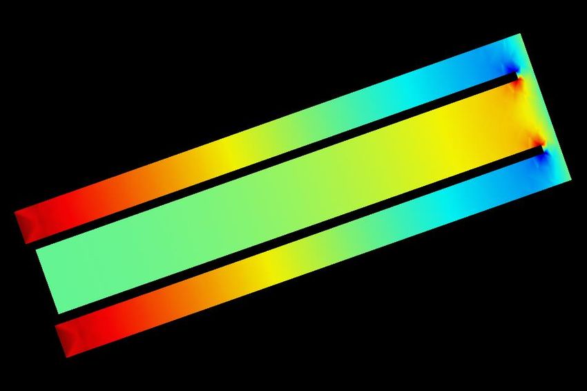
Göteborg, Sweden 2020Bandwidth Improvement of a Piezoelectric Micro Energy Harvester JOHAN ANDERSSON © JOHAN ANDERSSON, 2020 Master’s thesis 2020:35 Department of Mechanics and Maritime Sciences Division of Dynamics Chalmers University of Technology SE-412 96 Göteborg Sweden Telephone: +46 (0)31-772 1000 Cover: Stress distribution on the surface of the energy harvester. Chalmers Reproservice Göteborg, Sweden 2020
Bandwidth Improvement of a Piezoelectric Micro Energy Harvester
Master’s thesis in Applied mechanics
JOHAN ANDERSSON
Department of Mechanics and Maritime Sciences
Division of Dynamics
Chalmers University of Technology

                                               Abstract
Energy harvesting is a technology where electricity is generated from ambient energy resources. A piezoelectric
energy harvester, which converts vibrations to electricity, is a promising power supply for sensors connected to
the Internet of Things (IoT). This kind of power supply is self sustainable and does not need any maintenance
nor external fuels.
    The aim of this study is to propose a harvester design with large bandwidth for an IoT application on
micro scale. The eigenfrequencies and frequency response of the harvester are predicted by finite element
simulations and the simulation model is compared to experimental data. An electromechanical model (EMM)
is compared to a simplified pure mechanical model (PMM) and a correlation is found between the two models.
The frequencies are shifted by a factor 0.95, i.e. fEMM /fPMM = 0.95, and 1 mV corresponds to 7 MPa.
    Key factors for bandwidth improvement are a small eigenfrequency gap and a high enough voltage level.
The eigenfrequency gap is reduced with a back folded cantilever beam design with similar beam lengths and
constant uniform thickness. For a given amplitude of the vibration source the total voltage output can be
increased with a smaller coverage of piezoelectric material.
    Improved bandwidth is shown for three different beam lengths. The tolerance from the centre frequency is
about ±1 %, which corresponds to a 114 Hz bandwidth in the 4100 Hz region.

Keywords: Energy harvesting, Piezoelectricity, MEMS, Bandwidth

                                                       i
ii
Preface
This thesis is the final step to a Master of Science in Engineering. The work is based on studies in Engineering
Physics and Applied Mechanics at Chalmers University of Technology during 2014-2020.

                                       Acknowledgements
For the completion of this project I would like to express my gratitude to my supervisor Associate Prof.
Peter Folkow. During the entire period I have got great support and important advice to help me proceed.
When problems have occurred we have had constructive discussions to find new solutions. I would also like
to thank Lic. of Engineering Agin Vyas for useful input on the fabrication process. Furthermore thanks to
Associate Prof. Per Lundgren and Prof. Peter Enoksson for sharing your knowledge and experience in the field
of electronics and micro energy harvesters.

                                                                                  Johan Andersson, June 2020

                                                       iii
iv
Nomenclature
Abbreviations

COMSOL            A finite element simulation software
EMM               Electromechanical model
IoT               Internet of Things
MEMS              Microelectromechanical systems
PMM               Pure mechanical model
PZT               Lead zirconate titanate

List of symbols

Ai                Piezoelectric area on inner beam [m2 ]
Ao                Piezoelectric area on outer beams [m2 ]
bf                Bandwidth [Hz]
C                 Damping matrix
d                 Oscillation amplitude [m]
f                 Frequency [Hz]
f0                Eigenfrequency [Hz]
fd                Damping frequency [Hz]
K                 Stiffness matrix
li                Inner beam length [m]
lm                Outer proof mass length [m]
 0
lm                Inner proof mass length [m]
lo                Outer beam length [m]
M                 Mass matrix
t                 Time [s]
tb                Beam thickness [m]
tm                Proof mass thickness [m]
tp                PZT layer thickness [m]
U                 Voltage [V]
U                 Surface average voltage [V]
w                 Displacement [m]
wg                Gap between inner and outer beam [m]
wi                Inner beam width [m]
wo                Outer beam width [m]

α                 Mass damping coefficient [1/s]
β                 Stiffness damping coefficient [s]
∆f                Eigenfrequency gap [Hz]
ζ                 Damping ratio [-]
σ                 Stress [Pa]
σ                 Surface average stress [Pa]
ω                 Angular frequency [rad/s]

                                                      v
vi
Contents

Abstract                                                                                                                                                                                        i

Preface                                                                                                                                                                                       iii

Acknowledgements                                                                                                                                                                              iii

Nomenclature                                                                                                                                                                                   v

Contents                                                                                                                                                                                      vii

List of Figures                                                                                                                                                                               ix

List of Tables                                                                                                                                                                                ix

1 Introduction                                                                                                                                                                                 1
1.1 Background . . . . . . . . . . . . . . . . . . . . . . . . . . . . . . . . . . . . . . . . . . . . . . . . .                                                                               1
1.2 Aim . . . . . . . . . . . . . . . . . . . . . . . . . . . . . . . . . . . . . . . . . . . . . . . . . . . . .                                                                              3
1.3 Limitations . . . . . . . . . . . . . . . . . . . . . . . . . . . . . . . . . . . . . . . . . . . . . . . . .                                                                              3

2 Method                                                                                                                                                                                       3
2.1 Geometry . . . . . . . . . . . . . . . .          .   .   .   .   .   .   .   .   .   .   .   .   .   .   .   .   .   .   .   .   .   .   .   .   .   .   .   .   .   .   .   .   .   .    3
2.2 Finite element analysis . . . . . . . . .         .   .   .   .   .   .   .   .   .   .   .   .   .   .   .   .   .   .   .   .   .   .   .   .   .   .   .   .   .   .   .   .   .   .    4
2.2.1 Electromechanical model (EMM) . .               .   .   .   .   .   .   .   .   .   .   .   .   .   .   .   .   .   .   .   .   .   .   .   .   .   .   .   .   .   .   .   .   .   .    5
2.2.2 Pure mechanical model (PMM) . . .               .   .   .   .   .   .   .   .   .   .   .   .   .   .   .   .   .   .   .   .   .   .   .   .   .   .   .   .   .   .   .   .   .   .    5
2.2.3 Damping . . . . . . . . . . . . . . .           .   .   .   .   .   .   .   .   .   .   .   .   .   .   .   .   .   .   .   .   .   .   .   .   .   .   .   .   .   .   .   .   .   .    5
2.3 Simulation strategy . . . . . . . . . . .         .   .   .   .   .   .   .   .   .   .   .   .   .   .   .   .   .   .   .   .   .   .   .   .   .   .   .   .   .   .   .   .   .   .    5
2.3.1 Computation of eigenfrequencies . .             .   .   .   .   .   .   .   .   .   .   .   .   .   .   .   .   .   .   .   .   .   .   .   .   .   .   .   .   .   .   .   .   .   .    5
2.3.2 Computation of frequency response               .   .   .   .   .   .   .   .   .   .   .   .   .   .   .   .   .   .   .   .   .   .   .   .   .   .   .   .   .   .   .   .   .   .    6
2.4 Post processing . . . . . . . . . . . . .         .   .   .   .   .   .   .   .   .   .   .   .   .   .   .   .   .   .   .   .   .   .   .   .   .   .   .   .   .   .   .   .   .   .    6

3 Results                                                                                                                                                                                      7
3.1 Model validation to experiments       .   .   .   .   .   .   .   .   .   .   .   .   .   .   .   .   .   .   .   .   .   .   .   .   .   .   .   .   .   .   .   .   .   .   .   .   .    7
3.2 Comparison of EMM and PMM .           .   .   .   .   .   .   .   .   .   .   .   .   .   .   .   .   .   .   .   .   .   .   .   .   .   .   .   .   .   .   .   .   .   .   .   .   .    8
3.3 Eigenfrequency analysis . . . . .     .   .   .   .   .   .   .   .   .   .   .   .   .   .   .   .   .   .   .   .   .   .   .   .   .   .   .   .   .   .   .   .   .   .   .   .   .    9
3.4 Voltage level . . . . . . . . . . .   .   .   .   .   .   .   .   .   .   .   .   .   .   .   .   .   .   .   .   .   .   .   .   .   .   .   .   .   .   .   .   .   .   .   .   .   .   10
3.5 Bandwidth . . . . . . . . . . . .     .   .   .   .   .   .   .   .   .   .   .   .   .   .   .   .   .   .   .   .   .   .   .   .   .   .   .   .   .   .   .   .   .   .   .   .   .   13

4 Discussion                                                                                                                                                                                  17

References                                                                                                                                                                                    19

                                                                          vii
viii
List of Figures
 1.1    Schematic relation between voltage and frequency. If the eigenfrequencies are close to each other
        the inter peak valley rises. . . . . . . . . . . . . . . . . . . . . . . . . . . . . . . . . . . . . . . .      2
 1.2    A two degree of freedom cantilever design. The ends of the outer beams are attached to a fixture.               2
 2.1    Sketch of harvester design with definition of design parameters. The structure is symmetric
        about the dashed line. . . . . . . . . . . . . . . . . . . . . . . . . . . . . . . . . . . . . . . . . .        4
 2.2    Side view of the outer beam and proof mass. The beam consists of two layers: PZT (dark) and
        silicon (light). . . . . . . . . . . . . . . . . . . . . . . . . . . . . . . . . . . . . . . . . . . . . . .    4
 2.3    Mesh of the computational domain. . . . . . . . . . . . . . . . . . . . . . . . . . . . . . . . . . .           4
 2.4    Definition of bandwidth. The dashed line indicates the threshold level of 100 mV and the
        bandwidth is the frequency range of which the voltage is higher than the threshold. . . . . . . .               6
 3.1    Voltage output from the EMM for different damping ratios, based on Shen et al. [15] . . . . . .                 7
 3.2    Ratio between voltage from the EMM and stress from the PMM. . . . . . . . . . . . . . . . . .                   8
 3.3    Eigenfrequency gap as a function of beam length ratio. . . . . . . . . . . . . . . . . . . . . . . .            9
 3.4    Eigenfrequency gap as a function of proof mass thickness. . . . . . . . . . . . . . . . . . . . . .            10
 3.5    Electric potential distribution of one of the outer beams. . . . . . . . . . . . . . . . . . . . . . .         11
 3.6    Mode shape with tension and compression on the surface of the outer beams. Deflection not to
        scale. . . . . . . . . . . . . . . . . . . . . . . . . . . . . . . . . . . . . . . . . . . . . . . . . . . .   11
 3.7    Voltage output from the outer beams. The beams are covered with piezoelectric material from
        the attachment boundary to a length with given ratio of the outer beam length lo . . . . . . . .               12
 3.8    Electric potential distribution of the inner beam. . . . . . . . . . . . . . . . . . . . . . . . . . .         12
 3.9    Voltage output from the inner beam. The beam is covered with piezoelectric material from the
        outer proof mass boundary to a length with given ratio of the inner beam length li . . . . . . .               13
 3.10   Voltage output for lo = 2000 µm. . . . . . . . . . . . . . . . . . . . . . . . . . . . . . . . . . . .         14
 3.11   Voltage output for lo = 3000 µm. . . . . . . . . . . . . . . . . . . . . . . . . . . . . . . . . . . .         15
 3.12   Voltage output for lo = 4000 µm. . . . . . . . . . . . . . . . . . . . . . . . . . . . . . . . . . . .         15
 3.13   Voltage output for lo = 3000 µm and tm = 40 µm. . . . . . . . . . . . . . . . . . . . . . . . . . .            16
 3.14   Voltage output for lo = 3000 µm and li = 2900 µm. . . . . . . . . . . . . . . . . . . . . . . . . .            17

List of Tables
 3.1    Dimensions for the EMM and PMM comparison. . . . . . . . . . . . . . . . . . . . .             . . . . . .      8
 3.2    Design parameters for final design. All dimensions are in µm. . . . . . . . . . . . . .        . . . . . .     13
 3.3    Eigenfrequency gap, piezoelectric area coverage (absolute and relative), bandwidth and         tolerance
        for the three studied cases of different beam lengths. . . . . . . . . . . . . . . . . . .     . . . . . .     14

                                                          ix
1 Introduction
The modern society requires electricity in order to work. In our digital era more and more units are connected
to the so called Internet of Things (IoT). These units need electric supply, but some units cannot be connected
to the mains. Furthermore these units often have sensors that are either small or located in areas which are
hard to access. Batteries are not a suitable choice in that sense since they need maintenance, which can be
either hard or even impossible. The electricity must be generated from some self sustainable device. An energy
harvester is such a device. It generates electricity from ambient energy resources, such as vibrations, without
any external fuels. The key idea is to let each IoT unit have its own small power plant, where the power plant
is an energy harvester.
IoT applications with small sensors require energy harvesters on micro scale [1]. Electromagnetic harvesters,
which are efficient for macro scale applications, cannot be easily scaled down. Miniaturisation of magnets and
coils leads to fabrication issues as well as significantly decrease in efficiency. The piezoelectric energy harvester
is more suitable and beneficial for micro scale applications [2].
This thesis work investigates the opportunity to harvest energy on micro scale. The study is developed from
previous work made by Vyas [3] and Staaf [4].
1.1 Background
A piezoelectric material is a material that generates electricity from mechanical stress. The effect is due to the
crystalline structure of the material. When a stress is applied the piezoelectric material gets polarised and an
electrical charge is induced [5]. Lead zirconate titanate (PZT) is one of the best materials with respect to high
piezoelectric properties. Furthermore PZT is flexible and ductile, which means that it has a good mechanical
workability. These properties make PZT a suitable material for piezoelectric energy harvesters in general, and
for micro scale devices in particular [6].
The output from a piezoelectric energy harvester is maximised at its resonance frequency, even called
eigenfrequency. Therefore every harvester must be designed with an eigenfrequency that coincides with the
frequency range for a particular application. One of the most challenging issues is the significant output
decrease when the vibrational frequency slightly shifts. The narrow bandwidth makes the harvester inefficient
since most applications have some frequency variation [7].
One way to increase the bandwidth, i.e. harvestable frequencies, is to attach several single cantilevers to
the vibration source in an array. The cantilevers should have eigenfrequencies that are slightly shifted from
each other in order to cover the operating frequency spectrum. Even though each cantilever has a narrow
bandwidth their overlap result in a total wide bandwidth [8]. However, for this solution only one cantilever
generates electricity at a time which makes the design inefficient. Furthermore another disadvantage is that the
design requires much space if the harvester is to cover a wide range of frequencies, since that requires many
cantilevers [4].
Another way to increase the bandwidth is to make a design such that the eigenfrequencies are close to
each other. If the eigenfrequency gap, ∆f , is small enough the inter peak valley rises according to Figure 1.1.
Hence the range of continuous frequencies with high voltage increases as the inter peak valley rises, i.e. the
bandwidth increases [4]. The eigenfrequency gap can easily be reduced with a two degree of freedom cantilever
design, which consists of two main beams and one secondary beam [9]. The design is shown in Figure 1.2.
The outer, main beams, are attached to a fixture which is subjected to vibrations. A proof mass is put at the
connection link between the beams and at the end of the inner, secondary beam. This two degree of freedom
design generates a higher total output and a wider bandwidth than the array of equivalent single degree of
freedom cantilevers [10]. Furthermore the backfolded design enables the energy harvester to be small and area
efficient. This planar design is possible and desirable for fabrication on micro scale [4].
1voltage
∆f
frequency
Figure 1.1: Schematic relation between voltage and frequency. If the eigenfrequencies are
close to each other the inter peak valley rises.
Figure 1.2: A two degree of freedom cantilever design. The ends of the outer beams are
attached to a fixture.
21.2 Aim
The aim of this thesis is to develop a functional design for a piezoelectric energy harvester on micro scale for an
IoT application. A design is considered functional if the harvester generates a significant voltage for a large
range of frequencies. The design development starts from a backfolded two degree of freedom design, which is
promising with respect to bandwidth improvement. Results from this study will contribute to future fabrication
of functional piezoelectric energy harvesters on micro scale.
The design development is divided into several tasks. Two proposed simulation models are investigated
for the electromechanical analysis of the device. These models include assumptions which the rest of the
development are based on. Furthermore design parameters of the device, such as length and thickness, are
related to eigenfrequencies, eigenfrequency gap and voltage output. Finally the main task is to propose a design
that is promising with respect to large bandwidth.
1.3 Limitations
This study is limited to cover geometric and electromechanical analysis of the energy harvester. The two studied
models are an electromechanical model (EMM) and a pure mechanical model (PMM), and the harvester is
simplified to only include two materials; silicon and PZT. Furthermore the vibration source is simplified to
harmonic motion with constant amplitude. The behaviour of the energy harvester is predicted by simulations
in COMSOL Multiphysics 5.5. Since fabrication of microelectromechanical systems (MEMS) are hard and time
consuming it is considered to be outside the scope of this thesis. Nevertheless all dimensions of the device are
subjected to fabrication ability.
2 Method
The start point of the design development was a study by Vyas et al. [1]. From that study the proposed design
was promising with respect to small eigenfrequency gap and fabrication ability. In the following sections the
geometry of the design is defined and the assumptions of the finite element analysis, together with boundary
conditions, are stated. Furthermore it is followed by a brief description of the simulation strategy and the post
processing.
2.1 Geometry
The key design concept of this study was a backfolded and in plane two degree of freedom structure. The
structure consists of two outer and one inner cantilever beam, as well as one outer and inner proof mass. The
outer beams are clamped to a fixture which is subjected to vibrations from its surroundings. A sketch of the
design is presented in Figure 2.1. In the figure the proof masses are indicated by the light areas.
In the study by Vyas et al. the fabrication process of a piezoelectric micro energy harvester is described.
The beams consisted of several thin layers of different materials. These were, from top to bottom, 100 nm
platinum, 20 nm titanium, 1 µm PZT, 100 nm LaNiO, another 100 nm and 20 nm of platinum and titanium,
500 nm silicon dioxide and finally 20 µm silicon. The proof masses were made of a 500 nm silicon dioxide layer
and the rest was silicon [1]. The choice of materials was simplified into two models for this study, where the
simplification was based on materials with significant layer thickness, i.e. silicon and PZT. For the first model
the cantilever beams were simplified to a two layered material model. One layer of silicon and one layer of
PZT, where the PZT thickness tp was set to 1 µm. Both proof masses were considered one layer of silicon. In
the second model the entire structure was considered to be made of silicon. A layer overview with parameter
definitions is presented in Figure 2.2.
Due to fabrication abilities the thicknesses of the cantilever beams must be equal and constant, i.e. no
spatial variations. Fabrication of the beams were constrained to 20 µm thickness at the time of this study
(tb = 20 µm) [11]. Similarly the proof masses must have equal and constant thicknesses, but it may differ from
the cantilever beam thickness. In order to guarantee free motion of the cantilever beams the distance between
the beams, wg , must be at least 50 µm. Finally the smallest in plane feature size is 5 µm [12].
3lm
li lo
0
lm
wi wg wo
Figure 2.1: Sketch of harvester design with definition of design parameters. The structure
is symmetric about the dashed line.
tp
tb
tm
lo lm
Figure 2.2: Side view of the outer beam and proof mass. The beam consists of two layers:
PZT (dark) and silicon (light).
2.2 Finite element analysis
The finite element analysis was carried out with COMSOL Multiphysics 5.5. Since the structure is very thin
with respect to its length, the structure was treated as a shell. Two dimensional shell elements were used for
the computation which reduced the total degrees of freedom to be solved for. Due to symmetry in the geometry
only half the structure was considered during the simulations. Figure 2.3 shows the meshed computation
domain. The edge of the outer beam had a prescribed harmonic out of plane motion with no rotation. Since
the device can be orientated on the vibration source in a way such that pure out of plane motion is obtained,
Figure 2.3: Mesh of the computational domain.
4this assumption was made without loss of generality. The prescribed displacement w was defined by a given
amplitude d and angular frequency ω = 2πf according to
w(t) = d sin ωt. (2.1)
Two different types of analyses were performed for the simplified model presented in section 2.1. For the first
model a piezoelectric electromechanical analysis was performed and a pure mechanical analysis was performed
for the second model.
2.2.1 Electromechanical model (EMM)
In this model the structure was considered as a layered shell. The silicon layer was set to be linear elastic
and the PZT layer was set to be piezoelectric. The four parts, inner and outer beams and proof masses, were
connected with a continuity boundary condition. Electric insulation enclosed the beams and no electric currents
were allowed in the silicon proof masses. The interface between the silicon and PZT in the beams was set to
ground potential.
2.2.2 Pure mechanical model (PMM)
In the PMM the entire structure was made of silicon. The material was considered to be linear elastic. For
comparisons with the electromechanical model the total thickness of the beams was equal for both models, i.e.
the PZT layer from the electromechanical model is replaced by silicon of the same thickness.
2.2.3 Damping
Mechanical damping was added for the linear elastic and piezoelectric materials for both models. Rayleigh
damping was used for this study, where the damping matrix C is a linear combination of the mass and stiffness
matrices of the system, M and K
C = αM + βK. (2.2)
Here α and β are given by
ζ1 fd2 − ζ2 fd1
α = 4πfd1 fd2 2 − f2 , (2.3)
fd2 d1
ζ2 fd2 − ζ1 fd1
β= 2 − f2 ) , (2.4)
π(fd2 d1
where ζi is the damping ratio at frequency fdi [13]. The damping frequencies were chosen to be the same as the
first and second eigenfrequency, since damping is necessary where the response is large. The choice of damping
model was not further investigated and for this study the damping ratios ζ1 and ζ2 were assumed to be equal.
2.3 Simulation strategy
The simulations were divided into two subtasks. The first subtask was to find the first and second eigenfrequency
of the structure. When the eigenfrequencies were determined the following subtask was to compute the frequency
response for a frequency range including the eigenfrequencies. These two subtasks were connected to the
following problems: get the eigenfrequencies close enough and the voltage output high enough.
2.3.1 Computation of eigenfrequencies
The first two eigenfrequencies, f01 and f02 , were computed with the eigenfrequency solver in COMSOL. Different
design parameters, such as width, length and thickness of the beams and proof masses, were varied with a
parametric sweep. With this strategy the eigenfrequencies were computed for several designs in one single
run. The eigenfrequency gap ∆f = f02 − f01 was computed for each set of design parameters. A design was
considered useful if ∆f was less than 5 % of the centre frequency, average of first and second eigenfrequency.
52.3.2 Computation of frequency response
The determination of eigenfrequencies was followed by a frequency response study. In this step the frequency
of the prescribed motion in (2.1) was varied, and the response was solved for the stationary solution for each
frequency. The frequency range was chosen such that both eigenfrequencies were covered, with an additional
span of 2 % on each side.
2.4 Post processing
Post processing of the simulation results was divided into two parts. Extraction of quantities of interest from
the computed solution and data handling. The extraction part was carried out in the COMSOL results interface
and Matlab 2018b was used for the other part.
For the EMM the voltage on the top of the PZT layer was computed. In order to get voltage as a function
of frequency a surface average was calculated to be the actual output. To avoid cancellation effects as the inner
and outer beams might vibrate with shifted phase, the beams were treated as two separate systems. Hence the
total voltage output was the sum of the absolute values from each contribution.
U = |U in | + 2|U out | (2.5)
Similarly the beams were treated as two separate systems for the PMM. Instead of voltage a surface average
of the stress was computed on the top of the silicon beams. Since the motion of the structure ideally was
pure out of plane, the stress tensor had the major contribution from the component which coincided with the
length of the structure. The output measure was simplified to only regard that component, which also allowed
distinction between compression and tension for the surface average calculation.
σ = |σ in | + 2|σ out | (2.6)
In order to compare the output from different designs the bandwidth bf was introduced as the measure
of interest. This measure was related to a threshold level of 100 mV, which is the required useful voltage
for electric circuits in micro scale. Voltages above this threshold was considered to be harvestable [14]. An
illustration of the bandwidth is presented in Figure 2.4. A design with larger bandwidth was considered better,
regardless of peak voltage or inter peak valley voltage.
voltage
bf
frequency
Figure 2.4: Definition of bandwidth. The dashed line indicates the threshold level of
100 mV and the bandwidth is the frequency range of which the voltage is higher than the
threshold.
63 Results
The presentation of the results is divided into several parts. Firstly there are two sections about reliability of
the simulation models. The following two sections are about design strategies that make an effective energy
harvester. In the final section the previous results are used to propose an energy harvester design with improved
bandwidth.
Three types of COMSOL simulation models were used: 3D solid, multilayered shell and single layered shell.
The 3D solid and multilayered shell models simulated the EMM with silicon and PZT. Three dimensional
tetrahedral elements were used in the solid model and two dimensional triangular elements were used in the
shell model. The latter element type was also used in the single layered shell simulation model, but the only
material was silicon according to the PMM. All three models gave similar results but the 3D solid model had a
100 times longer computation time due to more elements. The multilayered shell model is a special feature
in COMSOL which only was available for a limited time during this project. Most results in this study was
therefore computed with the single layered shell model.
All simulations included a mesh size study. The aim of that study was to check convergence of eigenfrequencies
and voltage/stress, in order to guarantee that an appropriate mesh size was used.
3.1 Model validation to experiments
Experiments have been performed on a single cantilever beam made of silicon and PZT by Shen et al. [15].
The device was on micro scale with similar geometric dimensions and materials as the energy harvester in the
scope of this thesis. In order to validate the relevance of the assumptions in the EMM, the experimental results
were reproduced by COMSOL simulations of the EMM. The oscillation amplitude d was set to 0.12 µm, which
corresponds to an acceleration of 1.0 g. The eigenfrequency from the simulations was 468 Hz, while 461 Hz
was the measured eigenfrequency from the experiments. In Figure 3.1 the voltage output from the EMM is
presented for some damping ratios ζ used in the study by Shen et al. From the figure it is clear that the peak
value is strongly dependent of the choice of damping ratio. However the order of magnitude of the voltage
180
160
140
120
100
80
60
40
20
0
467 467.5 468 468.5 469 469.5 470
Figure 3.1: Voltage output from the EMM for different damping ratios,
based on Shen et al. [15]
7output from the simulations is similar to the measured data from the experiments by Shen et al. [15]. Based
on these experimental data, the oscillation amplitude and damping ratio in the following simulations were set
to d = 0.12 µm and ζ = 10−3 .
3.2 Comparison of EMM and PMM
Simulations were run for the EMM and PMM with the same geometry. The geometries that were studied were
different beam thicknesses, lengths of the outer beam and thicknesses of the proof masses. All combinations
of the dimensions presented in Table 3.1 were used, which resulted in a total of 175 different designs. The
restriction of tb = 20 µm was unknown when these simulations were run, which is the reason why variations of
tb are included. In an early stage of this project a beam length ratio of 0.98 was found to be beneficial with
respect to eigenfrequency gap reduction. Due to that the length of the inner beam was 98 % of the outer beam
length in this comparison. Furthermore the impact of proof mass thickness to eigenfrequency gap was not yet
investigated, which motivates why tm in this model comparison was chosen differently to the final thickness in
section 3.5. A more thorough investigation of ∆f is presented in section 3.3. Except for the parameters in
Table 3.1 and the inner beam length li , all other design parameters were constant for this comparison.
Table 3.1: Dimensions for the EMM and PMM comparison.
tb + tp [µm] 21, 26, 31, 36, 41
lo [µm] 2500, 2750, 3000, 3250, 3500, 3750, 4000
tm [µm] 50, 62.5, 75, 87.5, 100
The eigenfrequencies were shifted between the models. However, the quotient f0EMM /f0PMM was approxi-
mately 0.95 for both the first and second eigenfrequency for all designs. Further on the start and stop frequencies
of the frequency response analysis was related to the eigenfrequencies of each model. There were 61 frequencies
in the range of analysis for all designs and models. Figure 3.2 shows the relation between the EMM voltage and
the PMM stress for each frequency. Each frequency has 175 points which correspond to the different designs.
The relation is most uncertain at the eigenfrequencies and there is less variation for the other frequencies. An
14
12
10
8
6
4
2
0 10 20 30 40 50 60
Figure 3.2: Ratio between voltage from the EMM and stress from the PMM.
8average of the quotients results in a conversion factor of 7 mV/MPa, with an average error of 13 %.
Based on these results the following simulations were simplified to only use the PMM. The voltage was
approximated by the stress according to
U = 7 · 10−9 σ (3.1)
and the frequencies were shifted by a factor of 0.95.
3.3 Eigenfrequency analysis
The eigenfrequencies of the energy harvester were computed according to section 2.3.1. It was found that the
length of the beams had the most significant impact on the eigenfrequencies. Longer beams resulted in lower
eigenfrequencies and vice versa. The gap between the first two eigenfrequencies was strongly dependent on
the ratio between the lengths of the inner and outer beams, li /lo . Figure 3.3 shows how the eigenfrequency
gap changes for varying beam length ratios for three different beam lengths. The eigenfrequency gap was
minimised when the beams had approximately equal length. Furthermore ∆f was increased when the proof
mass thickness tm was increased. Since tb is restricted to 20 µm an equal thickness of beam and proof mass
sections was the best configuration with respect to minimising ∆f , which is shown in Figure 3.4. Finally it was
found that a small gap width, wg , between the beams was beneficial with respect to small ∆f .
0.4 0.5 0.6 0.7 0.8 0.9 1 1.1 1.2 1.3
Figure 3.3: Eigenfrequency gap as a function of beam length ratio.
915 20 25 30 35 40 45 50 55
Figure 3.4: Eigenfrequency gap as a function of proof mass thickness.
3.4 Voltage level
Factors that affect the voltage level were investigated in order to meet the requirements of bandwidth, stated
in section 2.4. The choice of damping ratio has a big impact, which is shown in section 3.1. Furthermore larger
oscillation amplitudes results in increasing voltages. However, since the determination of damping ratio is
uncertain without experimental measurements and the oscillation amplitude is application dependent, those
factors were set constant for the voltage level investigation.
Results from section 3.2 suggests a relation between stress and induced voltage. Due to geometry and
motion of the device, the stress varies along the length of the beam, while stress variations across the beam
width are considered negligible. The corresponding electric potential distribution along the length of the
outer beam is presented in Figure 3.5. The eigenfrequencies of the considered structure were 1773 Hz and
1816 Hz. For frequencies below the first eigenfrequency there was pure tension (or compression) and for higher
frequencies there was a mix of tension and compression along the beam. An example of the mode shape
with mixed tension and compression is shown in Figure 3.6. The useful output voltage from an electrode
is the average potential from the entire beam surface. Thus a mixture of tension and compression on the
same beam is not desirable, since some contributions to the total output is cancelled out for that particular
frequency. Consequently the total voltage depends on how much of the beam that is covered with piezoelectric
material. However the information of the potential distribution in Figure 3.5 does not tell anything about the
relation between piezoelectric coverage and output, since the potential changes sign at different beam lengths
for each particular frequency. For some frequencies the major output contribution comes from the attached
end of the beam and for other frequencies the major contribution comes from the proof mass end of the beam.
Different piezoelectric coverage ratios were investigated and Figure 3.7 shows the frequency response. The
voltage decreases for increasing piezoelectric coverage. However, smaller coverage implies less generated current
and thus less power. Therefore it would be desirable to go for a large piezoelectric coverage, but still reach a
significant voltage level with respect to a threshold of 100 mV.
10Figure 3.5: Electric potential distribution of one of the outer beams.
Figure 3.6: Mode shape with tension and compression on the surface of the outer beams.
Deflection not to scale.
11450
10 %
400 30 %
50 %
70 %
350
100 %
300
250
200
150
100
50
0
1720 1740 1760 1780 1800 1820 1840 1860
Figure 3.7: Voltage output from the outer beams. The beams are covered with piezoelectric
material from the attachment boundary to a length with given ratio of the outer beam
length lo .
Similarly the electric potential distribution for the inner beam is presented in Figure 3.8. On the contrary
to the outer beam, the inner beam has pure tension (or compression) along its entire beam length. The beam
length is measured from the outer proof mass. The frequency response for the inner beam is shown in Figure
3.9. In comparison to the outer beams the inner beam generates a lower voltage. Furthermore the inner beam
is not as effective at both eigenfrequencies as the outer beams.
Figure 3.8: Electric potential distribution of the inner beam.
12200
10 %
180 30 %
50 %
160 70 %
140
120
100
80
60
40
20
0
1720 1740 1760 1780 1800 1820 1840 1860
Figure 3.9: Voltage output from the inner beam. The beam is covered with piezoelectric
material from the outer proof mass boundary to a length with given ratio of the inner
beam length li .
3.5 Bandwidth
The development of a design proposal with respect to large bandwidth was based on the results from the
eigenfrequency analysis in section 3.3 and the voltage level analysis in section 3.4. The bandwidth problem was
a combination of these two parts. Firstly, in order to get the interaction effect from the two eigenfrequency
peaks, the eigenfrequency gap ∆f had to be small enough. Furthermore the voltage level had to be high enough
to reach above the threshold level. Since no experiments were performed in this study the oscillation amplitude
and damping ratio was chosen according to the validation in section 3.1, i.e. d = 0.12 µm and ζi = 10−3 .
The solution of the eigenfrequency part was achieved with equal beam and proof mass thickness, smallest
allowed beam gap width and similar beam lengths. All parameters that were constant throughout the simulations
are presented in Table 3.2. Since the entire structure was chosen to have the same thickness, tp of 1 µm was
neglected for simplicity. With the same reason the inner proof mass length lm 0
had no importance for this
geometry.
Table 3.2: Design parameters for final design. All dimensions are in µm.
tb 20
tm 20
wg 50
wo 200
wi 400
lm 100
Simulations were run for three different beam lengths, in order to investigate three different frequency areas.
For each case the inner beam length was adjusted to reduce ∆f . The voltage output for these three cases
are shown in Figure 3.10, 3.11 and 3.12. All figures show the contribution from the inner beam and the two
outer beams, as well as the total output. The green dotted line indicates the threshold level of 100 mV. In
order to get an output above the threshold the piezoelectric coverage was changed according to section 3.4.
13Since a larger piezoelectric area generates a higher current, and thus higher power, it was desirable to have as
large piezoelectric area as possible. The results from the three studied cases, including eigenfrequency gap,
piezoelectric area and bandwidth, are summarised in Table 3.3. The tolerance is the maximum deviation from
a design frequency which ensures a harvestable output.
Table 3.3: Eigenfrequency gap, piezoelectric area coverage (absolute and relative), band-
width and tolerance for the three studied cases of different beam lengths.
lo [µm] li [µm] ∆f [Hz] Ao [mm2 ] Ai [mm2 ] Ao [%] Ai [%] bf [Hz] tolerance [%]
2000 2000 79 0.80 0.32 100 40 114 ±1.4
3000 2990 16 1.20 0.36 100 30 23 ±0.6
4000 3980 5 1.12 0.16 70 10 8 ±0.4
600
Inner beam
Outer beams
500 Total
400
300
200
100
0
3950 4000 4050 4100 4150 4200 4250
Figure 3.10: Voltage output for lo = 2000 µm.
14300
Inner beam
Outer beams
250 Total
200
150
100
50
0
1850 1860 1870 1880 1890 1900 1910 1920 1930 1940 1950
Figure 3.11: Voltage output for lo = 3000 µm.
250
Inner beam
Outer beams
Total
200
150
100
50
0
1060 1070 1080 1090 1100 1110 1120
Figure 3.12: Voltage output for lo = 4000 µm.
15In order to illustrate the effects from the beam length ratio and the proof mass thickness on the final output,
non optimal values with respect to reducing ∆f were chosen for the 3000 µm design. In the first case tm was
set to 40 µm and in the second case li = 2900 µm. The same piezoelectric coverage was used as for the proposed
design, i.e. 100 % for the outer beams and 30 % for the inner beam. The results are presented in Figure
3.13 and Figure 3.14. The voltage level is similar to the proposed 3000 µm design in Figure 3.11 around the
eigenfrequencies, but much lower in the inter peak area. There is no rising inter peak valley effect for these
non optimal choices of tm and li , and consequently no significant bandwidth improvement. This illustrates the
importance of a small ∆f .
300
Inner beam
Outer beams
250 Total
200
150
100
50
0
1650 1700 1750 1800 1850 1900 1950 2000 2050 2100 2150
Figure 3.13: Voltage output for lo = 3000 µm and tm = 40 µm.
16300
Inner beam
Outer beams
250 Total
200
150
100
50
0
1750 1800 1850 1900 1950 2000 2050 2100 2150
Figure 3.14: Voltage output for lo = 3000 µm and li = 2900 µm.
4 Discussion
The results from the simulated EMM are shown to be similar to the the experimental results by Shen et al. for
a single cantilever piezoelectric micro energy harvester [15]. With the same materials, silicon and PZT, in the
present work it is most likely that the EMM will be a good match to future experiments for the behaviour of a
two degree of freedom design as well. Results from the simulations will be realistic in the sense of order of
magnitude. The comparison between the EMM and PMM shows that there is a correlation between stress and
voltage. This correlation motivates why the simplification of mechanical analysis is valid to predict the output
voltage. However, there are uncertainties in the choice of damping model and oscillation amplitude which
have a significant impact on the final output. Furthermore the damping may also be oscillation amplitude
dependent.
The eigenfrequency gap, ∆f , is shown from the frequency response analysis to have big impact on the
bandwidth. ∆f has to be rather small in order to get a rising inter peak valley effect. Similar beam lengths
and uniform constant thickness of the device are promising factors in order to reduce ∆f , which is the major
contribution from this project to future work. The peak voltage level is lower in the low frequency region
which makes it harder to find a design with output above the threshold. This can be solved with reduced PZT
coverage, with a reduced power output as an assumed drawback. For the three studied designs the relative
bandwidths are similar with a tolerance of about ± 1 %. Since each design is application dependent and works
for different frequencies, no design is considered better with respect to bandwidth. However, all the three
proposed designs show an improvement of bandwidth for three different frequency areas.
A drawback with the PMM is that nothing is told about the electric power. The simulation model must in
some way include electricity and a circuit connection. There is probably a trade off between the voltage and
power output, which is related to the PZT coverage on the beams. That would be the next thing to investigate.
In order to make any further conclusions, experimental measurements on a fabricated harvester are necessary.
The results from this study can predict promising candidates for a given vibration application (frequency and
amplitude), but the simulation model is too uncertain to give precise quantitative results. The most crucial
part is application dependent damping model. A suggestion for future work is to fabricate a pure silicon device
and measure the deflection in operation. This fabrication is much faster and cheaper than fabrication of the
17full electronic device. However the mechanical properties are still similar, which implies reliable measurements
for the damping model calibration.
Another thing that may be interesting to investigate is an attachment of the inner beam instead of the
outer beams. This two degree of freedom device may remain the effect of closing the first two eigenfrequencies,
but maybe result in other stress distributions than the ones presented in this study.
18References
[1] A. Vyas et al. A Micromachined Coupled-Cantilever for Piezoelectric Energy Harvesters. Micromachines
9.252 (2018). doi: 10.3390/mi9050252.
[2] K. Tao et al. “Micro electret-based power generator for ambient vibrational energy harvesting”. Energy
harvesting: Technology, methods and applications. Nova Science Publishers, 2016, pp. 23–24.
[3] A. Vyas. “Towards an on-chip power supply”. Licentiate thesis. Chalmers University of Technology, 2019.
[4] H. Staaf. “Conjoined piezoelectric harvesters and carbon supercapacitors for powering intelligent wireless
sensors”. PhD thesis. Chalmers University of Technology, 2018.
[5] J. A. Gallego-Juarez. Piezoelectric ceramics and ultrasonic transducers. Journal of Physics E: Scientific
Instruments 22.10 (1989), 804–816. doi: 10.1088/0022-3735/22/10/001.
[6] M. Kimura, A. Ando, and Y. Sakabe. “Lead zicronate titanate-based piezo-ceramics”. Advanced piezoelectric
materials. Woodhead publishing limited, 2010, pp. 89–110.
[7] L. Tang, Y. Yang, and C. Soh. Toward Broadband Vibration-based Energy Harvesting. Journal of
Intelligent Material Systems and Structures - J INTEL MAT SYST STRUCT 21 (2010), 1867–1897. doi:
10.1177/1045389X10390249.
[8] H. Xue, Y. Hu, and Q. Wang. Broadband piezoelectric energy harvesting devices using multiple bimorphs
with different operating frequencies. IEEE Transactions on Ultrasonics, Ferroelectrics, and Frequency
Control 55.9 (2008), 2104–2108.
[9] H. Wu et al. A novel two-degrees-of-freedom piezoelectric energy harvester. Journal of Intelligent Material
Systems and Structures 24.3 (2013), 357–368. doi: 10.1177/1045389X12457254.
[10] L. G. H. Staaf et al. Modelling and experimental verification of more efficient power harvesting by
coupled piezoelectric cantilevers. Journal of Physics: Conference Series 557 (2014). doi: 10.1088/1742-
6596/557/1/012098.
[11] A. Vyas. Personal communication. Chalmers University of Technology, Department of Microtechnology
and Nanoscience, May 19, 2020.
[12] A. Vyas. Personal communication. Chalmers University of Technology, Department of Microtechnology
and Nanoscience, Feb. 19, 2020.
[13] Z. Song and C. Su. Computation of Rayleigh Damping Coefficients for the Seismic Analysis of a Hydro-
Powerhouse. Shock and Vibration (2017). doi: 10.1155/2017/2046345.
[14] P. Lundgren. Personal communication. Chalmers University of Technology, Department of Microtechnology
and Nanoscience, May 12, 2020.
[15] D. Shen et al. The design, fabrication and evaluation of a MEMS PZT cantilever with an integrated
Si proof mass for vibration energy harvesting. Journal of Micromechanics and Microengineering 18.5
(2008).
19DEPARTMENT OF MECHANICS AND MARITIME SCIENCES CHALMERS UNIVERSITY OF TECHNOLOGY Göteborg, Sweden www.chalmers.se
You can also read