BEREZINSKII-KOSTERLITZ-THOULESS TRANSITION IN AN AL SUPERCONDUCTING NANOFILM GROWN ON GAAS BY MOLECULAR BEAM EPITAXY - PHYSICS
←
→
Page content transcription
If your browser does not render page correctly, please read the page content below
Nanotechnology

PAPER

Berezinskii–Kosterlitz–Thouless transition in an Al superconducting
nanofilm grown on GaAs by molecular beam epitaxy
To cite this article: Guan-Ming Su et al 2020 Nanotechnology 31 205002

View the article online for updates and enhancements.

                            This content was downloaded from IP address 132.170.219.53 on 22/03/2020 at 17:45
Nanotechnology
Nanotechnology 31 (2020) 205002 (6pp) https://doi.org/10.1088/1361-6528/ab71ba
Berezinskii–Kosterlitz–Thouless transition
in an Al superconducting nanofilm grown on
GaAs by molecular beam epitaxy
Guan-Ming Su1, Bi-Yi Wu1, Yen-Ting Fan2, Ankit Kumar1,3,
Chau-Shing Chang4, Ching-Chen Yeh1, Dinesh K Patel1, Sheng-Di Lin2,6,
Lee Chow1,5 and Chi-Te Liang1,4,6
1
Department of Physics, National Taiwan University, Taipei 106, Taiwan
2
Department of Electronics Engineering, National Chiao Tung University, Hsinchu 300, Taiwan
3
Department of Physics, BITS-Pilani, K. K. Birla Goa Campus, Zuarinagar, Goa 403726, India
4
Graduate Institute of Applied Physics, National Taiwan University, Taipei 106, Taiwan
5
Department of Physics, University of Central Florida, Orlando, FL 32816, United States of America
E-mail: sdlin@mail.nctu.edu.tw and ctliang@phys.ntu.edu.tw
Received 11 December 2019, revised 30 December 2019
Accepted for publication 30 January 2020
Published 2 March 2020
Abstract
We have performed extensive transport experiments on a 4 nm thick aluminum (Al)
superconducting film grown on a GaAs substrate by molecular beam epitaxy (MBE). Nonlinear
current–voltage (I–V ) measurements on such a MBE-grown superconducting nanofilm show that
V∼I3, which is evidence for the Berezinskii–Kosterlitz–Thouless (BKT) transition, both in the
low-voltage (TBKT≈1.97 K) and high-voltage regions (TBKT≈2.17 K). In order to further
study the two regions where the I–V curves are BKT-like, our experimental data are fitted to the
temperature-induced vortices/antivortices unbinding model as well as the dynamical scaling
theory. It is found that the transition temperature obtained in the high-voltage region is the
correct TBKT as confirmed by fitting the data to the aforementioned models. Our experimental
results unequivocally show that I–V measurements alone may not allow one to determine TBKT
for superconducting transition. Therefore, one should try to fit one’s results to the temperature-
induced vortices/antivortices unbinding model and the dynamical scaling theory to accurately
determine TBKT in a two-dimensional superconductor.
Keywords: nanofilm, superconductivity, aluminum, two-dimensional, GaAs substrate
(Some figures may appear in colour only in the online journal)
1. Introduction long-range correlation of the order parameter in two dimen-
sions [1]. Nevertheless, the Berezinskii–Kosterlitz–Thouless
Superconductivity in two dimensions itself is an interesting (BKT) transition [2, 3] can occur in a two-dimensional (2D)
and fundamental issue. One of the most probable reasons for system and allows the establishment of quasi-long-range
this is that according to Mermin–Wagner theorem, continuous correlation of the order parameter. The BKT physics of
symmetries cannot be spontaneously broken at a finite superconductivity is probably best characterized by nonlinear
temperature in systems with sufficiently short-range interac- I–V dependences where I and V are the current flowing
tions in dimensions d2 [1]. In other words, Mermin– between the source and drain contacts and the voltage drops
Wagner theorem seems to prohibit the superconducting phase between two voltage probes, respectively. A small but finite
transition that accompanies a symmetry breaking and a resistance is found at temperatures below the transition
temperature TBKT [4, 5]. The reason for this is that in the BKT
6
Authors to whom any correspondence should be addressed. scenario, zero resistance is possible only in the zero current
0957-4484/20/205002+06$33.00 1 © 2020 IOP Publishing Ltd Printed in the UK
Nanotechnology 31 (2020) 205002 G-M Su et al
limit. Any small non-zero current exerts a force of opposite removing the native oxide on the GaAs substrate at 600 °C for
signs on vortices of opposite polarity, thereby breaking apart 20 min, at 580 °C we grew a 200 nm thick undoped GaAs
the most loosely bound vortex/antivortex pairs and resulting buffer layer. The Ga shutter was turned off. Subsequently, the
in a finite resistance (and voltage). In the region where the GaAs surface temperature was increased to 600 oC with no As
BKT physics manifests itself as the voltage V varies with flux (As shutter was off) for 3 min in order to transform the
Iα( T). The exponent α(T) is greater than 3 below TBKT and is GaAs surface into a Ga-rich condition. Most importantly, the
equal to 3 at TBKT [4, 5]. Therefore, it is useful to measure the treated sample was cooled down in the ultra-high-vacuum
nonlinear I–V curves of a superconducting film and find the chamber to 0 °C (see later) in order to prevent any surface
relation V∼I α( T) at various temperatures. When α(T)=3, oxidation. Aluminum nanofilm growth started after the resi-
one can experimentally determine TBKT. The BKT transition dual arsenic vapor in the chamber had been pumped away and
of superconductivity has been observed in various nanofilms the background pressure had been lower than 2×10⁻¹⁰ Torr.
such as Pb atomic films [5], monolayer NbSe2 [6], Ga thin In our MBE system, the growth rate of the Al films was about
films [7], and one-atom-layer Tl–Pb compound on 0.366 μm h−1. During the growth of an Al nanofilm, the
Si(111) [8]. GaAs substrate holder was not rotating, and no heater power
Aluminum (Al) is a sustainable material since it is the was applied in order to ensure a low growth temperature. We
most abundant metal on the Earth’s crust. Al ultrathin film has note that in our MBE system the minimum reading of our
already found a wide variety applications in surface-enhanced thermometer is 0 °C. We made sure that the thermometer
Raman scattering (SERS) [9], photocatalysis [10, 11], metal- reading was always 0 °C but in reality, the growth temper-
enhanced fluorescence [12], plasmonic devices [13, 14], the ature might as well be lower than 0 °C. In any case, the
electrode for quantum dot light emitting diodes [15], nano- growth temperature was substantially lower than that of the
cavity [16], UV–vis chiroptical activity [17], and super- nanofilm presented in our previous work (room temper-
capacitors [18]. Recent advances in sample preparation have ature) [20].
made it possible to grow high-quality Al film by molecular
beam epitaxy (MBE) [13, 14, 19, 20]. In particular, an epi-
2.2. Device geometry and stability
taxial Al film of atomic thickness can be grown on a GaAs
substrate by MBE [19, 20]. Such an Al nanofilm is ideal for The Al sample was processed into a Hall bar geometry.
probing 2D physics and topological, superconducting trans- Contact pads made by standard photo lithography are pre-
ition in two dimensions [2–8]. Here we report extensive pared for wire bonding. The key issue is that we use dilute AZ
transport measurements on a 4 nm thick Al film grown on a developer in order to avoid etching the Al nanofilm. For an
GaAs substrate by MBE. Interestingly, in the nonlinear cur- as-grown 4 nm thick Al nanofilm, there are about 17 atomic
rent–voltage (I–V ) measurements, we have observed V∼I3, layers. However, according to our previous work on a similar
evidence for the BKT transition both in the low-voltage Al nanofilm [20], there is a≈2 nm thick AlOx layer on top of
(TBKT≈1.97 K) and high-voltage regions (TBKT≈2.17 K). our Al nanofilm as shown in the TEM studies. When we
In order to further probe the two regions where the I–V further consider the surface roughness of our Al 4 nm thick
characteristics show BKT-like behavior, we fit our exper- nanofilm (see later), we estimate that there are 7–10 layers of
imental data to the temperature-induced vortices/antivortices Al atoms. The Al nanofilm devices are stable in air over a
model as well as the dynamical scaling theory. It is found that long period of time (over 14 months), possibly protected by
TBKT≈2.17 K determined from the data in the high voltage the overlaying AlOx layer which is formed when the Al wafer
regime is actually the correct transition temperature since it is was removed from the MBE chamber for ex situ processing.
consistent with those measured by the aforementioned mod-
els. Thus our experimental data strongly suggest that one
2.3. Low-temperature four-terminal resistance measurements
should fit one’s experimental results to both the vortices/
antivortices unbinding model and dynamical scaling model The low-temperature transport experiments were performed
since the nonlinear I–V data (V∼I3) alone may not allow one in an Oxford Triton 200 cryo-free He3/He4 dilution refrig-
to unequivocally determine the topological transition temp- erator. The magnetic field is perpendicularly applied to the
erature TBKT. plane of the Al nanofilm. Although the base temperature of
our bottom-loading dilution refrigerator is around 13 mK, the
lowest measurement temperature was set at 250 mK. The
2. Experimental reason for this is that when the sample undergoes a
superconductor/metal transition at a high critical current,
huge heat dissipation can occur, and at a temperature below
2.1. Al nanofilm grown by MBE
250 mK the cooling power of our fridge is lower than heat
The semi-insulating GaAs substrate was first baked in our dissipation of our device, leading to an abrupt increase of the
Varian Gen II MBE chamber at 200 °C for 8 h. The purpose measurement temperature.
of this process is to remove the moisture on the surface of the Standard four-terminal dc resistance measurements were
GaAs substrate. After that, the GaAs substrate was heated to performed on our Al sample. A Keithley 2400 current source
400 °C for 5 h to remove organic residue in a preparation was used to provide a constant current which flows between
chamber. The wafer was put back in the main chamber. After the source and drain contacts. A Keithley 2000 multi-meter
2Nanotechnology 31 (2020) 205002 G-M Su et al
Figure 2. A 5 μm×5 μm AFM image of the top surface of the 4 nm
thick aluminum film. Note that the scale bar ranges from −1.0
to 1.0 nm.
respectively. Both Hc2(T=0) and critical temperature Tc are
substantially higher those of bulk Al (0.01 T and 1.2 K). The
h
Ginzburg–Landau coherence length xGL = 4peHc2 (T = 0)
is
measured to be 22 nm.
3. Results and discussion
The 4 nm thick (as grown) Al film reported in this paper was
prepared in a Varian Gen-II solid-source MBE system [20].
The quality of the sample in this work is similar to those
reported in [20]. According to our previous studies [19, 20],
the thinnest continuous Al film which we can prepare is 3 nm
thick (as-grown). We decide to study a 4 nm thick Al nano-
film as we wish to further study an Al ultrathin film with a
slightly enhanced thickness.
Figure 2 shows a 5 μm×5 μm atomic force microscope
(AFM) image of the top surface of the 4 nm thick aluminum
film. The black regions could correspond to voids in the Al
nanofilm which are not conducting and therefore should not
affect the transport properties and superconductivity in our Al
nanofilm [20]. The root-mean-square (RMS) surface rough-
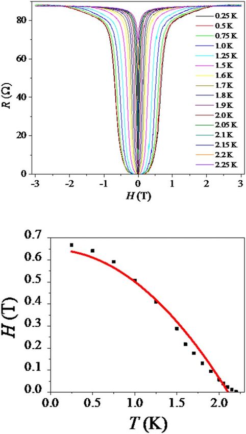
Figure 1. (a) Resistance measurements of the 4 nm thick Al film as a ness is measured to be 0.4 nm. This value is one order of
function of magnetic field R(H) for different temperatures T. (b) magnitude lower than that was reported in our previous work
Upper critical magnetic field as a function of temperature Hc2(T). [19]. The key issue is that in the present work, the growth
The fit corresponds to the theoretical models.
temperature (estimated to be much lower 0 °C) is lower than
that reported in [19] (room temperature). It may be possible
was used to measure the voltage difference between the that the low thermal energy provided by the substrate limits
voltage probes. the movement of Al atoms when they reach the substrate. In
some sense, the Al atoms are stuck onto the GaAs substrate at
2.4. Superconducting transition temperature and upper critical
a low growth temperature, thereby decreasing the RMS sur-
face roughness of Al film. This observation of decreasing
magnetic field
RMS surface roughness with decreasing substrate temperature
Figure 1(a) shows magnetoresistance measurements R(H) at in our Al film is consistent with Al nanofilms on steel grown
various temperatures. The magnetic field is applied perpend- by RF-magnetron sputtering [23] and Al ultrathin films on
icular to the plane of our Al nanofilm. For a certain temper- glass prepared by electron-beam evaporation [24].
ature, the upper critical magnetic field Hc2(T) can be measured Figure 3 shows the resistance measurements of the Al
when the magnetoresistance reaches half of the normal-state film as a function of temperature R(T) at zero magnetic field.
resistance value, and such results are shown in figure 1(b). When the resistance reaches the half value of its normal state,
There is a good fit Hc2(T)=HC2(0)[1-(T/Tc)2] [21, 22] to the the superconducting transition temperature is measured to be
data, though there appears to be small deviation from the fit in 2.2 K, which is substantially higher than that of bulk Al
the high T regime. The critical field Hc2(T=0) and critical (1.2 K). Normally the superconducting transition temperature
temperature Tc are measured to be 0.67 T and 2.21 K, of a thin film is lower than that of a bulk sample. However,
3Nanotechnology 31 (2020) 205002 G-M Su et al
Figure 3. Resistance of the 4 nm thick Al film as a function of
temperature R(T) at zero magnetic field.
the opposite trend, that is, an increased Tc measured in thin
films compared to those of bulk samples, has been observed
in double-atomic-layer Ga films on GaN [25], FeSe mono-
layer films on SrTiO3 [26] and FeSe on TiO2 [27]. These
interesting results, together with the present work on the
MBE-grown Al nanofilm, may indicate that the interface
effects play an important role in the enhanced superconductor
transition temperature in a nanofilm over that of its bulk
counterpart [28]. For example, it has been suggested that the
substrate plays an essential role in realizing the high-Tc
superconductivity in FeSe (48 K), probably via interface-
induced electron–phonon coupling enhancement and charge
transfer [27]. On the other hand, a FeTe ultrathin layer grown
Figure 4. (a) I–V curves at various temperatures on a log–log scale.
on a topological insulator substrate does not show super- The red lines correspond to linear fits V∼I α to the experimental
conductivity down to 5 K [28]. data. The two black dashed lines corresponds to V∼I3. (b) The
In our device, the Ginzburg–Landau coherence length is exponent α in the relation V∼I α obtained from the data shown in
estimated to be 22 nm, much longer than the as-grown Al film figure 4(a).
thickness (4 nm). Such results strongly suggest 2D super-
conductivity in our Al nanofilm. However, one may argue the
fit our experimental data to the temperature-induced vortices/
fact that the Ginzburg–Landau coherence length is much
antivortices unbinding model [29]
longer than the film thickness may not be sufficient for us to
claim 2D superconductivity. To this end, we perform exten- -2 b
Rµe T - TBKT , (1 )
sive V(I) measurements at different temperatures. The results
are shown in figure 4(a). The red lines represent fits V∼I α to where b is a constant. We obtain that the parameter TBKT is
the data at various temperatures. It is possible to obtain two from 2.16 to 2.2 K, with a slight current dependence which
fits over different regions for a fixed temperature. might be a consequence of weak Joule heating as shown in
The exponent α tends to decrease with increasing T. Inter- figure 5. However, such a small change of TBKT (0.04 K)
estingly, in sharp contrast to most experimental results observed in this sample over a magnitude of the current show
reported in the literature [4, 6–8], there are two regions that possible weak Joule heating in the normal state does not
showing behavior consistent with the BKT transition as prohibit us from determining the correct TBKT using the fits at
indicated by the two dashed lines in black (figure 4(a)). As a different currents. The measured TBKT is close to that mea-
result, there exist two regions in which the I–V curves show sured in the high-voltage region in the nonlinear I–V data.
BKT-like characteristics: TBKT=1.97 K in the low voltage As the measurement temperature approaches the critical
region and TBKT=2.17 K in the high voltage region as temperature Tc, the fluctuations of a system grow and more
shown in figure 4(b). time is required before the thermal equilibrium is reached.
In order to further study the two regions which show The characteristic length scale of the fluctuations is described
BKT-like behavior, we plot R(T) at zero magnetic field for by the correlation length x, and the critical behavior of
three different source-drain currents, as shown in figure 5. We elapsing time t takes the form: t µ x z. Since x approaches
4Nanotechnology 31 (2020) 205002 G-M Su et al
Figure 6. Scaling function (equation (2)) at different temperatures.
Figure 5. Resistance measurements as a function of temperature at The upper (lower) branch corresponds to below (above) the critical
three different source-drain currents. Red (blue) curves have been temperature. The discontinuity yields TBKT=2.17 K.
vertically offset by 10 Ω (20 Ω) for clarity. The continuous curves
correspond to a fit to equation (1).
reported in [4] and [6–8]. Perhaps by lowering the driving
infinity as T Tc, the time taken for thermalization hence current, two regions which show BKT-like behavior could
diverges. This phenomenon is called critical slowing down also be observed. We speculate that in our Al nanofilm the
and the exponent z is called the dynamical critical exponent. BKT-like characteristics in the low voltage region is caused
Fisher, Fisher, and Huse [30] derived a theory based on the by finite size effects [31]. In this context, near the resistive tail
universal scaling function for a d-dimensional super- in the low voltage region, free vortices, rather than unbound
conductor. According to [30], in our 2D Al nanofilm we have vortices/antivortices can be created [31].
1
I ⎛⎜ I ⎞⎟ Z ⎛ Ix ¢ ⎞
= P ⎜ ⎟ , (2 )
T ⎝V ⎠ ⎝T ⎠
4. Conclusion
where the symbol denotes above/below Tc, P is the scaling
function, x = x0 b
, and x¢ =
b
. Given that In summary, we have reported extensive transport measure-
T - TBKT T - TBKT ments on a 4 nm thick Al nanofilm on a GaAs substrate grown
Ix ¢
lim P+
x ¥
( ) constant, we
T
obtain V = (TBKT )-z I (1 + z) at by MBE. As our Al films can be grown on GaAs, we will be
able to integrate Al-based superconductivity, plasmonics,
TBKT. That is equivalent to V∼I3 with z = 2. In our case, the
trial value for parameters b, TBKT, and z are declared at first, SERS, light-emitting diodes, etc with existing GaAs HEMT
Ix
1 technology, which could be a great advantage for future
b
()
so x º TI e- ∣ T - T BKT ∣ and P T = T V can be calculated
I
()
I z
device applications. Interestingly, there appear to be two
by inputting the current and the corresponding voltage at a regions where the I–V curves are BKT-like. After fitting our
certain temperature. After that, P(x ) can be plotted. Our goal experimental data to both the temperature-induced vortices/
is to find a set of parameters (b, TBKT, z) so that P(x ) at antivortices unbinding model and the dynamical scaling the-
different temperatures collapse unto two branches. As shown ory, we conclude that the topological transition temperature
in figure 6, our analysis gives rise to a critical temperature TBKT=2.17 K measured in the high-voltage region is the
TBKT=2.17 K with a dynamical exponent z=2. Again, this correct one in our Al superconducting nanofilm. Our work
value is close to that determined in the V(I) data in the high- thus demonstrates that in order to unequivocally determine
voltage region the correct TBKT of superconducting transition, it is impera-
All the data and analysis shown in figures 5 and 6 as well tive to fit one’s data to not only the nonlinear I–V model but
as the experimental results in the linear transport regime also the temperature-induced vortices/antivortices unbinding
(figure 3) all give rise to a transition temperature of ∼2.2 K. model and the dynamical scaling theory.
These results strongly suggest that the topological transition
temperature determined in the high voltage regime as shown
in figure 4(b) is the correct TBKT » 2.17 K. Our experimental Acknowledgments
results strongly suggest that the relation V∼I3 at a certain
temperature alone may not be sufficient to accurate determine We thank Professor L-M Wang for useful discussions. We
the transition temperature. The two I–V regions that show would like to acknowledge the technical support from the
BKT-like behavior may have been observed in [5], though the Center of Nano Science and Technology and the Center of
authors did not mention this. It is not clear why I–V curves, Nano Facility at National Chiao Tung University. This work
which show BKT-like behavior in two regions V∼I3, are not was financially supported by the Ministry of Education
5Nanotechnology 31 (2020) 205002 G-M Su et al
(MOE) ATU program, National Taiwan University (NTU) [11] Zhou L, Tan Y, Wang J, Xu W, Yuan Y, Cai W, Zhu S and
(grant number: 108L892101), and the Ministry of Science and Zhu J 2016 Nat. Photon. 10 393–8
Technology (MOST) (grant number: MOST 105–2112-M- [12] Bauch M, Toma K, Toma M, Zhang Q and Dostalek J 2014
Plasmonics 9 781–99
002–005-MY3, MOST 108–2112-M-002–014-MY2, MOST [13] Chou B-T, Chou Y-H, Wu Y-M, Chung Y-C, Hsueh W-J,
108-2627-E-002-001, and MOST 108–2622–8–002–016) in Lin S-W, Lu T-C, Lin T-R and Lin S-D 2016 Sci. Rep. 6
Taiwan. The work of AK at NTU was made possible by 19887
arrangement with Professor E S Kannan at BITS-Pilani, India. [14] Cheng C-W, Liao Y-J, Liu C-Y, Wu B-H, Raja S S,
AK was supported by the TEEP@India Program provided by Wang C-Y, Li X, Shih C-K, Chen L-J and Gwo S 2018 ACS
Photonics 5 2624–8
the MOE, Taiwan (grant number: 106M4102–7). [15] Lee Y J, Kim H H, Lee Y J, Kim J H, Choi H-J and Choi W K
2019 Nanotechnology 30 035207
[16] Janisch C, Song H, Zhou C, Lin Z, Elías A L, Ji D,
ORCID iDs Terrones M, Gan Q and Liu Z 2016 2D Mater. 3 025017
[17] Liu J, Yang L, Zhang H, Wang J and Huang Z 2017 Small
2017 13 1701112
Lee Chow https://orcid.org/0000-0001-7729-6848 [18] Zai J, Liu Y, Li X, Ma Z-F, Qi R and Qian X 2017 Nano-Micro
Chi-Te Liang https://orcid.org/0000-0003-4435-5949 Lett. 9 21
[19] Lin S-W, Wu Y-H, Chang L, Liang C-T and Lin S-D 2015
Nanoscale Res. Lett. 10 71
References [20] Fan Y-T, Lo M-C, Wu C-C, Chen P-Y, Wu J-S, Liang C-T and
Lin S-D 2017 AIP Adv. 7 075213
[21] Gorter J C and Casimir H B 1934 Physika Z 35 963
[1] Mermin N D and Wagner H 1966 Phys. Rev. Lett. 7 [22] Bardeen J, Cooper L N and Schrieffer J R 1957 Phys. Rev. 108
1133–6 1175–204
[2] Berezinskii V L 1970 Zh. Eksp. Teor. Fiz. 59 907–20 [23] Mwema F M, Oladijo O P and Akinlabi E T 2018 Mater.
[3] Kosterlitz J M and Thouless D J 1973 J. Phys. C: Solid State Today: Proc. 5 20464–73
Phys. 6 1181–203 [24] Her S-C and Wang Y-H 2015 Indian J. Eng. Mater. Sci. 22
[4] Epstein K, Goldman A M and Kadin A M 1981 Phys. Rev. 268–72
Lett. 47 534–7 [25] Zhang H-M et al 2015 Phys. Rev. Lett. 114 107003
[5] Zhao W et al 2013 Solid State Commun. 165 59–63 [26] Ge J-F, Liu Z-L, Liu C, Gao C-L, Qian D, Xue Q-K, Liu Y and
[6] Xing Y et al 2015 Science 350 542–5 Jia J-F 2015 Nat. Mater. 14 285–9
[7] Wang H et al 2017 Nat. Commun. 8 394 [27] Ding H, Lv Y-F, Zhao K, Wang W-L, Wang L, Song C-L,
[8] Matetskiy A V, Ichinokura S, Bondarenko L V, Tupchaya A Y, Chen X, Ma X-C and Xue Q-K 2016 Phys. Rev. Lett. 117
Gruznev D V, Zotov A V, Saranin A A, Hobara R, 067001
Takayama A and Hasegawa S 2015 Phys. Rev. Lett. 115 [28] Eich A et al 2016 Phys. Rev. B 94 125437
147003 [29] Halperin B I and Nelson D R 1979 J. Low Temp. Phys. 36
[9] Lay C L, Koh C S L, Wang J, Lee Y H, Jiang R, Yang Y, 599–617
Yang Z, Phang I Y and Lin X Y 2018 Nanoscale 10 [30] Fisher D S, Fisher M P A and Huse D A 1981 Phys. Rev. B 43
575–81 130–59
[10] Lee M, Kim J U, Lee K J, Ahn S, Shin Y-B, Shin J and [31] Holzer J, Newrock R S, Lobb C J, Aouaroun T and Herbert S T
Park C B 2015 ACS Nano 9 6206–13 2001 Phys. Rev. B 63 184508
6You can also read