Characterization of Integrated Lumped Inductors and Transformers
←
→
Page content transcription
If your browser does not render page correctly, please read the page content below
Diplomarbeit

   Characterization of Integrated
        Lumped Inductors
        and Transformers

    Ausgeführt zum Zwecke der Erlangung des akademischen Grades eines
                      Diplom-Ingenieurs unter Leitung von

                  Werner Simbürger und Arpad L. Scholtz
                                     E389
          Institut für Nachrichtentechnik und Hochfrequenztechnik

              eingereicht an der Technischen Universität Wien
                          Fakultät für Elektrotechnik

                                      von

                             Ronald Thüringer
                                   9326356
                          Pretschgasse 21, 1110 Wien

Wien, im April 2002
Abstract

    The modern semiconductor industry has introduced constraints on circuit de-
signers for smaller as well as cheaper integrated circuits as the operating frequency
of application increases. An alternative, which helps to satisfy these requirements
is the use of on-chip inductors and transformers, improving the levels of perfor-
mance in bipolar and CMOS integrated circuits.
    In order to achieve the best performance, it is an essential task for the IC de-
signer to predict and optimize the electrical characteristics of the inductors and
transformers. This could be done by 3-D electromagnetic field simulation pro-
grams. But usually such simulations require very intensive computer calculations
which take a few hours to days. Therefore it is not possible to optimize the device
in a reasonable amount of time.
    In this thesis, techniques are introduced which allow a characterization of
inductors and transformers within a few minutes. The short calculation time
is achieved by using electrical lumped low-order models. The parameters of the
model are extracted from the geometrical structure of the inductor or transformer
by using FEM-Tools and analytical considerations. These techniques have been
compiled in a user-friendly software program FastTrafo v3.2.
    FastTrafo v3.2 provides the circuit designer a powerful environment to design
inductors or transformers on demand. The software delivers SPICE models based
on the technology and geometrical dimensions of the device. A verification of
the models shows a good agreement with several test objects. An inductor and a
transformer example are presented in this work.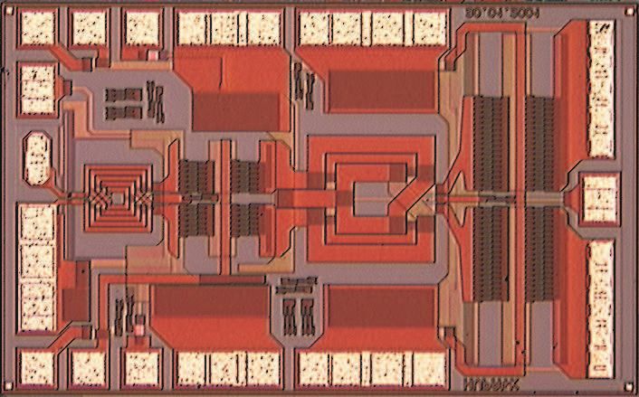
Contents

1 Introduction                                                                                                          1

2 Modeling                                                                                                              4
  2.1 Physical Layout . . . . . . . .   .   .   .   .   .   .   .   .   .   .   .   .   .   .   .   .   .   .   .   .   4
  2.2 Physical Model . . . . . . . .    .   .   .   .   .   .   .   .   .   .   .   .   .   .   .   .   .   .   .   .   6
  2.3 Low-Order Inductor Model . .      .   .   .   .   .   .   .   .   .   .   .   .   .   .   .   .   .   .   .   .   6
  2.4 Higher-Order Inductor Model       .   .   .   .   .   .   .   .   .   .   .   .   .   .   .   .   .   .   .   .   8
  2.5 Transformer Model . . . . . .     .   .   .   .   .   .   .   .   .   .   .   .   .   .   .   .   .   .   .   .   8

3 Parameter Extraction                                                                                                  12
  3.1 Inductance Calculation . . . . . . . .            .   .   .   .   .   .   .   .   .   .   .   .   .   .   .   .   12
  3.2 Serial Resistance . . . . . . . . . . .           .   .   .   .   .   .   .   .   .   .   .   .   .   .   .   .   14
  3.3 Substrate Resistance . . . . . . . . .            .   .   .   .   .   .   .   .   .   .   .   .   .   .   .   .   16
  3.4 Substrate Capacitance . . . . . . . .             .   .   .   .   .   .   .   .   .   .   .   .   .   .   .   .   19
  3.5 Oxide and Interwinding Capacitance                .   .   .   .   .   .   .   .   .   .   .   .   .   .   .   .   20
  3.6 Test-Structures and De-embedding .                .   .   .   .   .   .   .   .   .   .   .   .   .   .   .   .   26

4 Experimental Results                                                                                                  29
  4.1 A 4.7nH Inductor for 2 GHz . . . . . . . . . . . . . . . . . . . . .                                              29
  4.2 A 3:2 Transformer for 5.8 GHz . . . . . . . . . . . . . . . . . . .                                               36

5 Conclusion                                                                                                            42

A FastTrafo User Manual                                                                                                 43

Bibliography                                                                                                            70

Acknowledgements                                                                                                        72

                                        i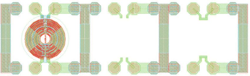
Chapter 1

Introduction

Today monolithic inductors and transformers are extensively used in different
types of integrated RF circuits. Incipiently, in earlier days they were realized as
discrete components. However increasing demands on the application side nom-
inate monolithic integrated inductors and transformers as a viable solution for
circuit design. This technique allows a realization of compact high frequency cir-
cuits with a high level of integrity along with low production costs.
Such typical applications of integrated inductors and transformers include for
example:

   • input and output matching networks for amplifiers

   • inductive loaded amplifiers

   • LC tank circuits of low phase noise voltage control oscillators

   • BALUN function in differential applications

Figure 1.1 and Fig. 1.2 show the schematic diagram and micrograph of a 5.8 GHz
power amplifier realized in a 25 GHz fT silicon technology. The circuit demon-
strates an application of on-chip transformers.
The circuit consists of an input transformer X1, a driver stage with cascode, an
interstage transformer X2 and an output stage with cascode. The input trans-
former X1 acts as balun as well as input matching network. The balun function
allows that the input signal can be applied balanced or single ended if one input
terminal is grounded. The transformer X2 acts as interstage matching network.
Basically all integrated components exhibit a non-ideal electrical behaviour. They
are afflicted with parasitic effects, especially in transformers. The ability to design
the circuits with optimum performance involves how to handle these parasitic
effects. The parasitics must be taken into consideration very careful. Therefore it
is necessary to characterize the components.

                                          1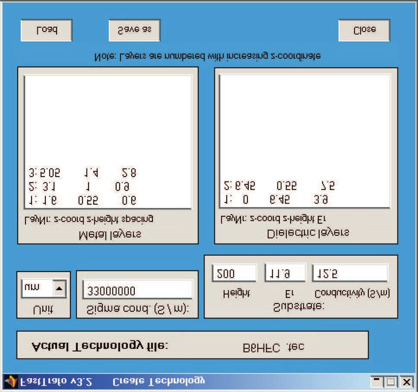
CHAPTER 1. INTRODUCTION                                                                                                    2

                      DB                              DC DCB    VCCD      OB                           OC OCB

                                       Driver Stage                X2                   Output Stage
               X1                                                 N=2:1
                                                                                                                    RFO+
              N=3:2                                        T3
                                  T1                                                   T8                     T10

                             T5           T6          T7                         T12        T13        T14

       RFI                        T2                                                   T9                     T11
                                                           T4
                                                                                                                    RFO-
                           DBG           DGND                                  OBG          OGND

             Figure 1.1: Schematic diagram of a 5.8 GHz power amplifier

              DCB          DC     DB             DGND                  OGND

                                                                                                             RFO+
                                                                  Interstage
                                                                 Transformer
               GND

                              Input    Driver Driver
                           Transformer Stage Cascode

                                                                                                             OBG
               RFI

                                                                                                             RFO-
               DBG

              OCB          OC     OB             VCCD                  OGND

Figure 1.2: Chip photograph of a 5.8 GHz power amplifier (size: 1.56 x 1 mm2 )

The complete electrical characteristic of monolithic transformers and inductors
can not be predicted by closed-form equations. Numerical methods must be used.
There exist many commercially available electromagnetic field solvers which com-
pute the field distribution of metal structures based on the Maxwell equations.
The disadvantage of such 3-D numerical solver is that a full field calculation con-
sumes ample amount of time. Therefore it is not possible to optimize inductors or
transformers by varying geometrical data of the structure in a reasonable amount
of time. Additionally, there exists a limitation that many solvers deliver only the
scattering parameters at the input and output ports. The scattering parameters
can not be used directly in a time domain or frequency domain circuit simulation
along with other active and passive, linear and nonlinear RF circuit elements. For
CHAPTER 1. INTRODUCTION 3 these reasons, it is convenient to develop different calculation methods to predict the electrical characteristics and to provide an equivalent model. In this work a computer program called FastTrafo v3.2 was developed, which allows fast and accurate prediction of the electrical characteristics of transform- ers and inductors in different semiconductor technologies. It is an improved and extended program version of FastTrafo v2.0 which was developed in an earlier master thesis [Kehrer 00]. The program version 3.2 additionally determines dif- ferent types and shapes of transformers and inductors. Further, new features of the program are provided, such as a stand alone application and new user in- terface. Furthermore, all calculations can be done without any other commercial software. Whereas, the earlier version 2.0 was restricted to MATLAB [Matlab 01]. In FastTrafo v3.2 the electrical characterization is done by a lumped low-order model of inductors or transformers. The parameters are extracted by using closed- form equations and finite element method tools. To get an electrical model from the physical structure the program user just has to specify dimensions and geo- metrical data of the structure, such as technology definition, used layers, number of turns, geometric dimensions and used layers. A comfortable input mask of the program and the fast model calculation allow the circuit designer to optimize the inductor or transformer for a specific RF application in short time. This power- ful feature avoids to develop inductor and transformer design libraries which are costly and inefficient. FastTrafo v3.2 provides the circuit designer with a full characterization of trans- formers. However, inductor models are still limited on inductance calculation in the actual version. The characterization of inductors treated in this work is avail- able in a preliminary version. The following chapters present the internal algorithms of FastTrafo which deter- mine the equivalent model parameters. Chapter 2 gives an overview on characterization of inductors and transformers. Basic electromagnetic effects are illustrated. Low order lumped models and an extension to generate higher order models are introduced. Chapter 3 gives basic information related to parameter extraction of the electri- cal parameters of low order lumped model. Two finite element tools, FastHenry [MIT 96] and FastCap [MIT 92], are introduced for inductance and capacitance calculation and their implementation in FastTrafo. Chapter 4 depicts two design examples and experimental results of an inductor and a transformer. Measurement results are compared to simulation results.
Chapter 2

Modeling

In this chapter equivalent models of planar inductors and transformers are derived
from the physical layout. It starts with a short overview of the physical effects
followed with the appropriate equivalent electrical models.

2.1     Physical Layout

            Figure 2.1: Schematic cross-section of a planar inductor.

Monolitic transformers and inductors are constructed using conductors inter-
wound in the same plane or overlaid on multiple stacked metal layers. They
can be implemented in circular or rectangular shapes with different winding con-
figurations. Each of these realizations exhibit specific performance advantages.

                                        4
CHAPTER 2. MODELING 5 There exist many publications which describe these possibilities in construction and optimization of inductors [Ashby 96], [Yue 98], [Niknejad 00] as well as of transformers [Rabjohn 89], [Long 00]. Independent of geometrical structures, their affect is always the same with respect to physical phenomena of the structures. Figure 2.1 shows a schematic three dimensional cross-section of an inductor. It gives an insight into the basic physical effects. The picture shows only two adjacent turns realized on one metal layer embedded in oxide. The conductors are separated from the substrate by oxide. This simplified model is sufficient to illustrate the different electromagnetic fields that are present in an integrated inductor when excited. Around the traces exists a time varying magnetic field B(t), created by the cur- rent flow in the metal. B(t) is responsible for the stored magnetic energy and the resulting inductance. Further, in case of transformers B(t) is responsible for coupling between the primary and secondary winding. However, there exists other electromagnetic fields that decrease the performance of inductors and transformers which result in losses due to the non ideal physical properties of the used materials. Each of the electric field components E1-E3 in Fig.2.1 results in loss of energy in the whole structure. E1(t) is the electric field along the metal trace. It is caused by the current in the winding and the finite conductivity. The current causes in association with ohmic losses a voltage drop along the whole winding and hence a voltage difference between each turn. This difference maintains the field denoted by E2(t) which is present between each turn. Due to the finite resistance and capacitive coupling a leakage current flows from turn to turn. In the same manner the electric field component E3(t) forces a leakage current between the metal traces and ground. In addition to the described electromagnetic fields, many other high-order effects are present. For instance, eddy currents arise in the metal traces and force a skin effect due to penetration of time varying magnetic fields. Further a proximity effect occurs due to the interaction between the magnetic field and currents. Both results in increased resistances and losses. Additionally currents induced in the substrate give rise to counterproductive secondary magnetic fields which interact with the primary magnetic field B(t).
CHAPTER 2. MODELING                                                                 6

2.2      Physical Model
An alternative for a fully 3-D field analysis is an approximation with electrical
lumped elements (R,L,C). This is valid because the physical lengths of the con-
ducting segments in the layout are typically much less than the guided wavelength
at the operation frequency. Due to this approximation, the analysis is reduced to
electrostatic and magnetostatic calculations instead of the complex electromag-
netic field solvers.
In a physical model each circuit element is related directly to the physical layout.
This property is very important when designing new inductors or transformers
where measurements data are not available.
The key to accurate physical modeling in this way is the ability to describe the
behaviour of the inductance and the parasitic effects. Each lumped element of
the model should be consistent with the physical phenomena occuring in the
part of structure it represents. In a pure physical model the value of electrical
lumped elements is only determined by the geometry and material constants of
the structure.
During modeling, we have to be prudent about the accuracy and limitations of
the model. The integration of several lumped elements gives only an estimation
of the electrical behaviour. It is clear that the number of elements determines the
grade of the approximation. With increasing number of elements the precision
increases. On the other hand the simulation time rises too. A trade-off between
accuracy and simulation time is vulnerable.

2.3      Low-Order Inductor Model
The aim of low-order models is to minimise the number of components in the
equivalent circuit. The following proposed low-order model allows a character-
ization of the inductor up to its first self resonant frequency. Around the self
resonant frequency, the model fails due to its low-order.
The basic idea is to model the whole winding as one lumped physical element
with two ports. Accordingly, the inductance and all parasitics just relate to one
physical element.
Which parasitics appear and how they have to be arranged in an equivalent
electrical circuit can be easily found by Fig. 2.2. The cross-section of a rectangular
inductor realized on two metal layers is shown.
The lumped elements can be identified as:

   • L, Inductance due to the magnetic flux.
   • RL , Ohmic loss in the conductor material due to skin effect, current crowd-
     ing and finite conductivity.
CHAPTER 2. MODELING 7
Oxide
CL
RL Substrate
Metal layer 2
L Topview
Metal layer 1
COx
CSub RSub P-
Ground plane P+
Figure 2.2: Three dimensional cross-section of a monolithic inductor
• CL , Parasitic capacitive coupling between the winding turns.
• CSub , Parasitic capacitive coupling into the substrate.
• COx , Parasitic capacitive coupling into the oxide.
• RSub , Ohmic loss in the conductive substrate.
Figure 2.3 shows the resulting equivalent circuit. It represents a symmetrical
pi-circuit with ports on both sides. The series branch consists of the overall in-
ductance L and serial resistance RL which appears along the whole winding. CL
is located between the terminals and represents the losses due to the capacitive
coupling from winding to winding. Because of the assumption of symmetry, the
other static parasitic elements COx , RSub , CSub of the winding are divided into
two equal parts and placed on each port side. This is expressed by
COx1 = COx2 = COx /2 (2.1)
CSub1 = CSub2 = CSub /2 (2.2)
RSub1 = RSub2 = 2RSub (2.3)
Note, that the capacitance CL models the parasitic capacitive coupling between
the input and output port of the inductor. The capacitive coupling is based on
the crosstalk between the adjacent turns. The capacitance allows the signal to
flow directly from the input to the output port without passing through the
inductor. Since the crosstalk effect depends on the potential difference between
the turns it is not trivial to determine the equivalent capacitor CL between the
ports. For modeling this capacitor it is necessary to take the voltage profile along
the winding into account.
All other parameters can be determined by statistical investigations of the induc-
tor structure.CHAPTER 2. MODELING 8
CL
P+ P-
L RL
COx1 COx2
C Sub1 RSub1 RSub2 C Sub2
Figure 2.3: Compact inductor model
2.4 Higher-Order Inductor Model
The use of additional circuit elements results in more accuracy in characterization
of the physical structure. This can be achieved by creating higher-order models.
Compared to the low-order model the lumped elements are not derived from
the impact of the whole winding. Furthermore the structure is sectioned into
multiple individual segments. Each of them will be characterized by an equivalent
subcircuit. The electrical behaviour of the whole inductor yields by joining the
subcircuits related to the physical structure. In a first approximation the inductor
winding can be divided into straight conductor elements.
Figure 2.4 shows such a rectangular spiral inductor divided into 8 segments. The
physical layout is partitioned into several coupled straight conductor lines. Each
line has a similar pi-equivalent circuit as the inductor illustrated in Fig. 2.3,
except the capacitor CL .
These lumped pi-elements are then joined serially to model the entire inductor
structure. Also the capacitive and inductive coupling between the segments must
be taken into account and considered as a capacitance between each segment and
as coupling factor between each inductance. Figure 2.5 shows the resulting high-
order model that results from physical structure Fig. 2.4. Note that the model
only considers the capacitive coupling between two adjacent parallel segments.
This approximation is valid since the capacitive coupling to the other segments
is very small.
2.5 Transformer Model
The operation of transformers is based upon the magnetic coupling between two
windings. Each winding, primary and secondary, has a self inductance LP , andCHAPTER 2. MODELING 9
2
6
3 7 5 1
8 P-
4 P+
Figure 2.4: Segmentized rectangular spiral inductor.
Segment 1 Segment 2 Segment 3 Segment 4
P+
Turn 1
Capacitive
Coupling P-
Turn 2
Segment 5 Segment 6 Segment 7 Segment 8
Figure 2.5: Inductor higher-order model
LS . The magnetic coupling between the windings is expressed by the mutual-
inductance M. In case of an ideal transformer this information is sufficient to
create an equivalent circuit, shown in Fig. 2.6.
Alternatively, from the specification of the mutual inductance, it is possible to
define a coupling coefficient k. It represents the strength of coupling between the
primary and secondary winding.
M
k=√ (2.4)
LP LSCHAPTER 2. MODELING 10
M
LP LS
Figure 2.6: Ideal transformer equivalent circuit
Generally, monolithic transformers are always afflicted with several loss mecha-
nisms which originate from the usage of non ideal materials. Since the construction
of monolithic transformers consists of two planar inductor windings realized in
the same manner as shown in the chapter before the same parasitic phenomena
take effect. An equivalent low-order transformer circuit can be found based on
the low-order inductor model Fig. 2.3.
Figure 2.7 shows the resulting equivalent low order transformer circuit [Kehrer 00].
Two low order inductor circuits are placed side by side. The magnetic coupling
between both windings is considered by a coupling factor k between the two
inductances. The parasitic coupling between the windings is considered by four
crossing capacitors Ckx .
The capacitive coupling within a winding is minor related to the capacitive cou-
pling between primary and secondary winding. Therefore the capacitor CL from
the inductor model is neglected in the transformer model.
The model exhibits a substantial approximation in frequency range starting from
DC up to 2/3 of the first self resonant frequency. For more accuracy a high order
model must be used which could be derived with the help of coupled conductors,
shown in section 2.4.CHAPTER 2. MODELING 11
P- P+
PRIMARY WINDING
CSubP2 CSubP1
R SubP2 COXP2 RP LP COXP1 R SubP1
CK4 CK3 CK2 CK1
R SubS2 COXS2 COXS1 R SubS1
CSubS2 RS LS CSubS1
Coupling Coefficient:
kPS (LP ,LS )
SECONDARY WINDING
S-
S+
Figure 2.7: Compact transformer modelChapter 3
Parameter Extraction
A lumped low-order model for inductors and transformers is found in chapter
2. This chapter describes the extraction of parameter method from the physical
structure.
3.1 Inductance Calculation
Inductance calculation of metal structures is based on the Maxwell equation.
~ ×H
▽ ~ = J~ + ∂t D
~ (3.1)
With this formula it is possible to derive an inductance value for arbitrary 3-D
structures. However in most cases, a closed form expression doesn’t exist. There-
fore numerical methods are used to solve the problem.
In our applications generally the frequencies of interest are quite low reducing the
problem to a magnetoquasistatic analysis. This assumption leads to inductance
expressions for coils and transformers which can be easily attained from known
basic inductance formulas. In [Kehrer 00] it is shown step by step how to get this
resulting expression starting from the magnetoquasistatic approximation.
The result is that each transformer or inductor can be analyzed with knowledge
of the self- and mutual inductances of individual conductor elements. Figure 3.1
shows a transformer with a turn ratio of n=2:2. The transformer structure can
be interpreted as a composition of several rectilinear conductors. The individual
conductor elements are consecutively numbered from 1 to 22. The trace with the
elements 1-11 represents the primary winding which consists of two turns. On
the left side is the primary port labeled with P+ and P-. The secondary winding
begins on the right side with the conductor element 12 and ends with element 22.
The secondary port is labelled with S+ and S-.
After splitting the transformer into a sequence of rectilinear conductors it is neces-
sary to get information about the self inductances from each segment and mutual
12CHAPTER 3. PARAMETER EXTRACTION 13
Figure 3.1: Square-shaped monolithic transformer with a turn ratio of n = 2 : 2.
inductances between each other. Appropriate formulas for self and mutual induc-
tances of straight conductors with rectangular cross section and constant current
density can be found in [Greenhouse 74] and [Grover 46]. With this information,
we are able to build inductance formulas for the whole transformer.
The self inductances of the primary winding LP and secondary winding LS is the
sum of all self inductances Li of the conductors in the particular winding plus the
sum of the mutual inductances Mi ,k between the conductors within one winding.
The complete self inductance of the windings can be written as
nP np −1 nP
X X X
LP = Li + 2 Mi,k (3.2)
i=1 i=1 k=i+1
nPX
+nS XS −1 npX
nP +n +nS
LS = Li + 2 Mi,k (3.3)
i=nP +1 i=nP +1 k=i+1
where i, k are the numbers of the individual conductors (i.e. For the secondary
winding in Fig. 3.1 the conductor numbers are i = 12 ... 22 ). It should be men-
tioned, that Mi ,k changes the sign depending on the current direction in the
segments. For instance, two parallel segments have a negative mutual coupling
and segments placed antiparallel a positive coupling.
The mutual inductance M between the two windings is the sum of the mutual in-
ductances of each primary conductor to each secondary conductor. The complete
mutual inductance between the windings can be written as
nP
X nPX
+nS
M= Mi,k (3.4)
i=1 k=nP +1
The summation indices represent the numbers of the individual conductors.CHAPTER 3. PARAMETER EXTRACTION 14
This approach to calculate the overall inductance by summing the inductances
from joined wire segments can be found in the literature known as Greenhouse
method [Greenhouse 74]. It is applicable as long as there exists self inductance
and mutual inductance expressions for the single segments. This is not a limita-
tion in our applications since the geometries of planar transformers and inductors
are based on rectangle- or polygon-shape turns which consists of rectilinear con-
ductors.
A similar algorithm in a more complex form is realized in the freeware program
FastHenry. FastHenry [MIT 96] is a program capable to compute self and mutual
inductances of arbitrary tridimensional conductive structures in a magnetoqua-
sistatic approximation. The algorithm used in FastHenry is an acceleration of a
mesh formulation approach. The internal resulting linear system from the mesh
formulation is solved using a generalized minimal residual algorithm with a fast
multipole algorithm to efficiently compute the problem. This allows a very short
calculation time. The user just has to specify an input file where the conductors
are defined as a sequence of rectilinear segments. The current distribution in the
structure will automatically be calculated by the program with the help of the
created meshes. Therefore the signs of the calculated mutual inductance are al-
ways correctly assigned. Hence the user is only constrained to handle the physical
dimensions and one doesn’t have to consider the current flow direction in each
segment. The resulting self and mutual inductance values relate on user defined
input ports. These terminals may be set by the user at any places along the metal
structure.
Due of short processing time and easy handling of the conductor elements, Fas-
tHenry is suitable for our applications. Therefore, the freeware program is pre-
ferred instead of our own Greenhouse algorithm in the software core of FastTrafo.
It provides an interface for generating appropriate FastHenry input files which
describe the transformer or inductor structures.
3.2 Serial Resistance
The ohmic losses in the winding are caused by finite conductivity of the metal.
An analytic estimation of the series resistance may be obtained from the basic
formula of straight rectangle conductors (Fig. 3.2).
l
R=ρ (3.5)
wh
where ρ represents the resistivity of the material [Ωm], l the total length [m] of
the winding and w, h the cross-section dimensions [m] of the winding trace.
The equation (3.5) is valid for a uniform current distribution along the cross-
section. This condition is fulfilled only for direct current and low frequencies. AtCHAPTER 3. PARAMETER EXTRACTION 15
Figure 3.2: Straight rectangular conductor
increasing frequencies the current density becomes more and more nonuniform
due to high frequency effects in the metal. They can by identified as skin and
proximity effect. The origin of both lies in penetration of time varying magnetic
fields in the metal.
During the phenomena of skin effect, the magnetic field in the metal is pro-
duced by the current flow in the conductor itself. The induced eddy currents in
the conductor force most of the current to flow near the boundary of the metal
conductor. In consequence of the higher current density on the edges, the serial
resistance increases with the frequency. A formula for the high frequency resis-
tance in rectangle conductors (Fig. 3.2) based on the direct current case given by
[Lofti 95].
1
!2 !5 10
f f
RAC = RDC 1 + + (3.6)
fl fu
s −2
πρ π2ρ h2
fl = , fu = K 1 − (3.7)
2µwh µh2 w2
where w, h are the cross-section dimensions [m], µ is the permeability [Vs/Am] of
the metal. RDC is the resistance [Ω] in the direct current mode. The frequencies
fl and fu [Hz] are the cutting frequencies of the low frequency case and of the
high frequency case. K is the elliptic integral first order
π
Z
2 1
K(x) = q dφ (3.8)
0 1 − x2 sin2 (φ)
In contrast to the skin effect, the proximity effect only occurs if at least two con-
ductors are present. The magnetic fields from each conductor affects the current
flow in the other, resulting in a non-uniform current distribution. The proxim-
ity effect is similar to the skin effect. Decrease of effective cross-sectional area ofCHAPTER 3. PARAMETER EXTRACTION 16
the conductor increases the resistance. In this case, the mathematical problem is
more complex due to the interaction of the second or more conductors. Hence, it
is not possible to solve the problem with a closed formula, as can be done in case
of skin effect and therefore numerical methods must be implemented.
In FastTrafo the serial resistance is calculated by the program FastHenry [MIT 96].
In addition to the inductances between defined terminals the software delivers the
effective serial resistances. The internal used algorithm is based on (3.5) which
assumes a uniform current density along the cross-section. However, it is possible
to take the skin and proximity effect into account. The whole cross-section of the
conductor is divided into a number of rectangle filaments (Fig. 3.3). The current
density inside each filament is assumed to be constant but the magnitude may
differ from filament to filament. An iterative algorithm considers the interaction
between the magnetic fields produced by each filament and the current in each
filament. The result is an approximation of the current distribution through a
bundle of filaments where each sustains a constant current density. With this
discretized current distribution and formula (3.5) it is possible for the program
to evaluate the equivalent series resistance of the whole conductor.
I
Figure 3.3: Conductor discretization into a bundle of filaments
It is evident that the accuracy of the approximation depends on the number of
discretized elements. But it should be mentioned that there exists a trade off
between the accuracy and processing time of the calculation.
3.3 Substrate Resistance
The substrate resistance represents the ohmic losses in the substrate. They are
caused by the current flow between the winding conductor and the ground con-
tact. Although the winding is embedded in a non-conducting dielectric, a current
flow is possible through the capacitive coupling between winding and substrate.
An appropriate expression for the substrate resistance is derived in [Kehrer 00].
The substrate resistance calculation is based on the area where the capacitiveCHAPTER 3. PARAMETER EXTRACTION 17
coupling acts on the substrate. This area depends on the width, thickness of the
winding and height position over the substrate material.
Figure 3.4 shows the cross-section of the winding. The winding is represented by
a full metal conductor.
Figure 3.4: Winding suspended in a dielectric above the substrate [Kehrer 00].
The substrate resistance can be written as [Kehrer 00]
1 π W + 6 HOX + T Wef f
RSub = ln 2 coth , for < 1 (3.9)
π σSub l 8 HSub HSub
π π W +6 HOX +T Wef f
RSub = / ln 2 e 4 HSub , for >1 (3.10)
4 σSub l HSub
where Wef f specifies the width [m] of the capacitive coupling area and is defined
as Wef f = W +6 HOX +T . W is the width [m] of the winding, HOx is the distance
[m] between the winding and substrate, T is the thickness [m] of the metal layer
and l is the mean perimeter [m] of the winding. HSub is the thickness [m] and
σSub the conductivity [S/m] of the substrate.
The definition of W and l is illustrated in Fig. 3.5. The approximation that the
winding can be interpreted as a full metal conductor instead of gaps between the
turns has been obtained by a field simulation.
In case of a transformer the primary and secondary winding must be handled
separately. Fig. 3.6 shows the decisive dimensions for applying 3.9 and 3.10. The
influence on the serial resistance of one winding through the interaction with the
second winding can be neglected.CHAPTER 3. PARAMETER EXTRACTION 18
Winding mean
perimeter l
Winding width W
Figure 3.5: Inductor: Definition of mean perimeter and winding width
Primary winding Secondary winding
W prim l prim W sec l sec
Figure 3.6: Transformer: Definition of mean perimeters and winding widthsCHAPTER 3. PARAMETER EXTRACTION 19
3.4 Substrate Capacitance
At low frequencies and in low-resistive substrates the parasitic effect is mainly
determined by the resistance of the substrate. With decreasing frequency or using
high-resistive substrates another material effect must be considered: parasitic
capacitive coupling into the substrate. This coupling effect can be taken into
account by a capacitor connected in parallel to the substrate resistor. With the
help of the substrate resistance from section 3.3 and substrate material constants
an expression will be derived in the following.
The electrical behaviour in the substrate material can be directly observed by
considering the configuration shown in Fig. 3.7. It shows a substrate material
block placed between two ideal conductor plates. The electrical equivalent circuit
of the physical configuration consists of the resistor RSub and the shunt-capacitor
CSub .
Figure 3.7: Substrate block and equivalent circuit.
The electrical resistance between the plates can be expressed by
h
RSub = ρ (3.11)
A
where ρ represents the resistivity [Ωm] of the substrate, h height [m] of the sub-
strate block and A [m2 ] the base area of the block.
Beside the resistance, there exists a capacitance between the conductor plates. It
can be derived from the well-known plate capacitor formula
A
CSub = ǫr ǫ0 (3.12)
h
where ǫ0 is the permittivity of free space [As/Vm] and ǫr the relative permittivity
of substrate [1], h height [m] of the substrate block and A [m2 ] the base area of
the block.CHAPTER 3. PARAMETER EXTRACTION 20
It is noticeable that 3.11 and 3.12 include the same geometric factor h/A or its
reciprocal. Substituting the geometric factors yields
RSub CSub = ρ ǫr ǫ0 (3.13)
Formula 3.13 represents now a relation between the resistance and capacitance
independent on the geometric form of the material block. Hence the substrate
capacitance follows the conventional knowledge of the substrate resistance and
material constants.
Another relevant point of interest is the expression on the right side of (3.13). It
represents the inherent time constant of the material. The reciprocal leads to the
cut-off frequency fC of the material
ωC 1 1
fC = = = (3.14)
2π 2πρǫr ǫ0 τSub
where τSub [s] represents the material time constant.
The cut-off frequency marks the frequency border where the capacitance in-
fluences in the substrate are no longer negligible. For instance, a typical high
doped silicon substrate material with ρ=18.5 Ωm and ǫr = 11.9 keeps the cut-off-
frequency fC =8.14 GHz.
3.5 Oxide and Interwinding Capacitance
The oxide and inter winding capacitance are based on electrostatic parameter
extraction. For a fast extraction, it is useful to make the following two assumptions
in the physical structure of the inductor or transformer to simplify calculations:
• The typical resistivity in the underlying substrate is significantly smaller as
in oxide material. This allows the approximation to replace the substrate
with ideal conductor material.
• The second simplification results from the cross-section of the windings.
The form is always the same, independent on the position of the cut (Fig.
3.8). In accordance to the form, the static capacitance distribution along the
winding is uniform. Once the capacitances per unit length is determined, it
is then possible by using the average length to get an expression for the static
capacitances of the structure. This assumption reduces the 3-dimensional
problem to a 2-dimensional one as a function of the cross-section.
With these two simplifications the capacitance calculation is reduced to a static
multiple coupled line analysis. The lines are buried in dielectrica without the exis-
tence of any lossy material. Many analytic formulas can be found in the literatureCHAPTER 3. PARAMETER EXTRACTION 21
Cut
(a) (b)
Figure 3.8: (a) 3-D Symmetrical inductor (b) Cross-section
for solving that problem. However in those formulas, there exists limitations in
shape and constellation of the conductors. The line constellation in the cross-
section of inductors and transformers is not always as symmetric as shown in
Fig. 3.8. In general the traces vary in their widths and spacings between each
other. The best and most accurate way to extract the capacitance from such
varying dimensions is the usage of capacitance extraction tools based on numer-
ical techniques. In FastTrafo the software tool FastCap [MIT 92] is used. It is a
freeware program developed by the MIT.
Oxide Capacitance Calculation
The following example shows a general way to calculate the parasitic capacitance
of different inductors or transformers. The calculation procedure is demonstrated
on a symmetrical inductor but can be implemented on all other types. The same
steps are realized in the software program FastTrafo.
Figure 3.9 shows the top view and cross-section of the inductor. The inductor con-
sists of a winding with three turns realized on two metal layers. The traces are
numbered from 1 to 3 beginning with the innermost turn. In the cross-section,
the layer and turn constellation located above the metal plane constitutes the
substrate material. This cross-section is the input information for the static ca-
pacitance calculation with the help of FastCap.
One turn in Fig. 3.9 always consists of two parallel metal layers. In the cross-
section this can be seen as two stacked metal lines. As they are on same potential
no capacitance arises in between. The capacitors C1’, C2’, C3’ represent the
capacitances per unit length between each trace and substrate, C12’ and C23’
between the traces. Their values are calculated using FastCap.
The total static oxide capacitance COx of the inductor is determined by theCHAPTER 3. PARAMETER EXTRACTION 22
Crossing area
Turn1 Turn2 Turn3
Figure 3.9: (a) Oxide capacitance calculation (b) Cross-section
capacitances per unit length C’ and mean lengths of the traces lm (3.15). Not
included in the mean lengths is the width of the crossing area wcr . The capacitance
in the crossing area must be considered as an extra term Ccr .
COx = C1′ lm1 + C2′ lm2 + C3′ lm3 + Ccr (3.15)
Since the field distribution in the crossing area is not uniform, an accurate value
for Ccr can only achieved by a 3-dimensional numerical extraction. To save cal-
culation time, it is recommended to estimate the value of the capacitance. A
first-order approximation can be done with the plate capacitor formula (3.16).
ǫA
C= (3.16)
d
Innerwinding Capacitance Calculation
In the low-order model of an inductor, the distributed capacitance across the
winding must be substituted by a single equivalent capacitor Cequ . The capaci-
tance value can be calculated by the stored electrical energy between the turns.
The resulting energy must be the same as in case of a single capacitor (Fig. 3.10).
The figure illustrates the distributed capacitance between the turns as lumped
capacitors. Their static capacitance values are based on turn to turn capacitance
per unit length, Fig. 3.9b. The capacitive coupling in the crossing area is neglected
for the innerwinding capacitance calculation.CHAPTER 3. PARAMETER EXTRACTION 23
The electrical energy stored in a capacitor is defined as:
C V2
E= (3.17)
2
where C is its capacitance and V denotes the voltage across the capacitor. By
applying (3.17) on each capacitor in Fig. 3.10, it is possible to determine the
whole stored energy between the turns.
To acquire the voltage on each capacitor, it is necessary to calculate the potential
along the winding which can be done determined by decomposing the inductor
into n-segments and connecting an AC voltage source as shown in Fig. 3.10a.
C’
v0 AC Crossing area
V0 Cequ
Figure 3.10: a)Distributed capacitance of the winding b)Equivalent capacitor
Each segment represents a conductor element with the inherent impedance
Zk = Rk + jωLk (3.18)
where Rk is the ohmic resistance, Lk represents the complete inductance of each
segment and ω the exciting frequency. Lk includes the self and all mutual induc-
tances which take effect on the conductor element. Determination of Rk and Lk
is described in section 3.2 and section 3.1 respectively.
All segments are connected in series. The voltage drop along one segment is
assumed to be constant. Leakage currents from the segments to ground or betweenCHAPTER 3. PARAMETER EXTRACTION 24
adjacent segments are neglected. For this reason, all segments carry same current
and the voltage drop on each segment Vk is proportional to their impedances Zk .
From the Kirchoff law, it follows that the summation over all n segments voltages
leads to the source voltage V0 .
n
X
Vk ∝ Zk V0 = Vk (3.19)
k=1
With these two relations, the voltage profile across the winding is well defined
and the voltage on each capacitor results from the potential difference between
two adjacent segments, where it is connected.
Figure 3.11: Two adjacent segments
Fig. 3.11 shows a section of the inductor with two adjacent parallel segments.
The stored electrical energy between the segments can be expressed by
C ′ lmbs ∆V 2
EP = (3.20)
2
where C’ represents the capacitance per unit length, lmbs the geometric mean
length of both segments and ∆V denotes the voltage difference between the seg-
ments. The shaded area in Fig. 3.11 represents boundary for energy calculation
using 3.20.
The total electrical energy stored in the winding EW results by summing all
partial electrical energies EP along the winding, which is calculated using 3.20.CHAPTER 3. PARAMETER EXTRACTION 25
X
EW = EP,k (3.21)
k
The equivalent capacitor must store the same electric energy EW as the winding.
From (3.22), (3.20) and (3.17) result in the capacitance value for the equivalent
capacitor Cequ
1 X ′
Cequ = 2
C lmbs,k ∆Vk2 (3.22)
V0 k
V0 represents the applied voltage between the two winding ports, C’ represents
the capacitance per unit length between the turns. lmbs,k is the mean length
between two adjacent parallel segments and Vk the potential difference between
these segments (Fig. 3.11).CHAPTER 3. PARAMETER EXTRACTION 26
3.6 Test-Structures and De-embedding
Before using monolithic inductors and transformers in integrated circuits it is rec-
ommended to characterize their performance by different measurements which is
usually performed with the help of a network analyzer. The network analyzer pro-
vides the scattering parameters which describe the electrical behaviour between
input and output ports of the test object(DUT). Often, these measurements are
performed directly on wafer. Although special RF frequency probes are used for
this task they can not be placed directly on the test object as the geometrical
dimensions of the probes rarely match with the ports of the test object. Therefore
the test object is embedded in a test structure with defined geometric dimensions
of the ports. However, these structures are afflicted with parasitic inductances
and capacitances which largely influence the measurement of the actual DUT.
In order to obtain the real S-parameters of the DUT, the parasitics have to be
characterized. Their influences must be subtracted from the measurement on the
test structure and the phenomena is referred to as de-embedding.
Test object (DUT): Transformer
Figure 3.12: Test structure: DUT, Open, Short
De-embedding: Short - Open Structure
The task of de-embedding is to mitigate the measured S-parameters data from
the parasitics of the test structure which are caused by the probe pads and metal
line, connected to the DUT. In our application, this is achieved by measuring
the S-parameters on two additional structures. In the first structure, the DUT
is replaced by a short in the second by an open. With these additional mea-
surements, it is possible to calculate the correct S-parameters of the DUT. The
correction procedure can be explained representing schematically, the circuit of
the test structure shown in Fig. 3.12.CHAPTER 3. PARAMETER EXTRACTION 27
DUT: Sparas. Y2
Z1 Z3
Port1 Y1 Z2 D.U.T Z4 Y3 Port2 .
SDUT
a)
Open: S open Y2
Z1 Z3
Port1 Y1 Z2 Z4 Y3 Port2
b)
Short: S short Y2
Z1 Z3
Port1 Y1 Z2 Z4 Y3 Port2
c)
Figure 3.13: Deembedding equivalent circuits: a)Dut b)Open c)Short
Figure 3.13a shows an equivalent circuit of the test structure with DUT. On theCHAPTER 3. PARAMETER EXTRACTION 28
left and right side of the DUT are the ports where the probes are placed during
the measurement. The DUT is symbolized by a two port box. The box is sur-
rounded by admittances and impedances which represent the additional parasitic
due to the test structure. The admittances Y1 , Y3 , represent the capacitive cou-
pling between the metal interconnections and the silicon substrate on each port,
Y2 the capacitive coupling between the ports. Z1 , Z3 , originate from the metal
interconnections series impedances between the ports of the test structure and
DUT while Z2 , Z4 represent the serial metal interconnections from the DUT to
ground.
Figure 3.13b shows the circuit in case of an open. The serial impedances Z1 -Z4
are not connected and hence neglected. Just the admittances Y1 , Y2 , Y3 remain
in the measurement.
Figure 3.13c shows the short de-embedding circuit. The impedances Z1 , Z2 and
Z3 , Z4 are connected between signal and ground.
With the three measured S-parameters sets Sparas. , Sshort , Sopen (Fig. 3.13) a
formula can be specified which leads to the correct S-parameter set SDU T of the
DUT which proceed from the impedance and admittance matrices. From the
conversion of the matrices exists the relations [Zinke 95]:
1 h i
Y = (E − S)(E + S)−1 (3.23)
Z0
h i
Z = Z0 (E + S)(E − S)−1 (3.24)
S = (Z/Z0 − E)(Z/Z0 + E)−1 (3.25)
S = (E − Z0 Y)(E + Z0 Y)−1 (3.26)
Z = Y−1 (3.27)
where Z0 is the characteristic impedance of the measurement system and E rep-
resents the identity matrix with ones on the diagonal and zeros elsewhere.
!
1 0
E=
0 1
As shown in Figure 3.13b the parasitic admittances Y1 -Y3 can be easily found
by the open configuration. For determination of parasitic impedances Z1 -Z4 , it is
necessary to consider the open and short configuration. The impedance matrix
with the parasitic impedances Z1 -Z4 yields from the subtraction of open and short
admittance matrices (3.28).
ZparsiticZ = (Yshort − Yopen )−1 (3.28)
Now, the correct Z-parameter of the DUT can be attained by subtracting ZparsiticZ .
ZDUT = (Yparas. − Yopen )−1 − ZparsiticZ (3.29)
Applying (3.25) yields the correct S-parameter of the DUT.Chapter 4
Experimental Results
In this chapter measurement results are compared to FastTrafo simulation results
which is done by example of an inductor and a transformer in silicon bipolar
technology. Further, in the first example, the increasing accuracy with a second
order model will be illustrated in comparison to the first order model.
The measurements of the transformer and inductor were performed by a two port
network analyzer in a Z0 = 50 Ω test system. The test structure and de-embedding
procedure were introduced in section 3.6. The network analyzer provides the
scattering parameters of the test object. With the help of the transformation
formulas 3.23 - 3.27, other relevant parameters of the test object can be derived.
4.1 A 4.7nH Inductor for 2 GHz
The inductor in this section consists of symmetrical winding with N=5 turns
(Fig. 4.1). The inductance is about 4.7 nH at low frequencies. The self resonant
frequency of the inductor is near to 7.3 GHz.
Figure 4.1: Winding scheme of the inductor
29CHAPTER 4. EXPERIMENTAL RESULTS 30 Figure 4.2: Metal structure and technologie cross-section of the inductor The inductor is fabricated in Si bipolar process B7HF. In this process, the metal layers are composed of aluminium (σ = 33e6 S/m) and are embedded in sili- condioxide SiO2 , with a relative permittivity of εr =3.9. The oxide is arranged over a p− - doped silicon substrate, which has a εr =11.9 and a conductance of 5.4 S/m. Although the process allows several metal layers, the winding resides just on one single metal layer. An additional second metal layer is only used for
CHAPTER 4. EXPERIMENTAL RESULTS                                                31

the interconnection between the turns. Fig.4.2 illustrates the metal structure of
the winding and a cross section from the technology.
With the given dimensions of the winding and the technology data, FastTrafo
provides a first order electrical model (Fig. 4.3) and a second order electrical
model (Fig. 4.4) of the inductor after parameter extraction. The electrical behav-
iour of these two models are compared to the data attained from the 2-port on
wafer measurement.

            Figure 4.3: First order equivalent circuit of the inductor

           Figure 4.4: Second order equivalent circuit of the inductor

Figure 4.5 and Fig. 4.6 display the scattering parameters S11 and S21. S11 rep-
resents the input reflection factor and S21 the transmission factor of the induc-
tor. Both parameters are simulated and measured in a frequency range between
f=200 MHz and f=13 GHz. The marks on the curves help to compare the values
CHAPTER 4. EXPERIMENTAL RESULTS 32
at the same frequencies. Both simulated models show the same basic frequency
behaviour as the measurement. The second order model is slightly closer to the
measured data, especially at higher frequencies.
Figure 4.5: Measured and simulated scattering parameter S11 of the inductor
Figure 4.7 and Fig. 4.8 show the real and the imaginary part of the reciprocal of
the admittance parameter Y11. The curves give the information about the input
impedance of the inductor when the second port is shorten to ground. This is a
very important exciting mode of the inductor which is often used in applications.
The maximum value of the real part indicates the parallel resonant frequency of
the inductor. The predicted resonant frequencies from the models at 7.2 GHz and
7.36 GHz are close to the measured values at 7.3 GHz.
Figure 4.9 illustrates the quality factor Q of the inductor at shorten output port.
Q can be expressed by the ratio between the imaginary and real part of the input
impedance.
Q = Im Y11−1 /Re Y11−1 (4.1)
Figure 4.10 shows the effective inductance between the two ports of the inductor
over the frequency. The inductance can be extracted from the input resistance at
shorten output by
L = Im Y11−1 /ω (4.2)CHAPTER 4. EXPERIMENTAL RESULTS 33 Figure 4.6: Measured and simulated scattering parameter S21 of the inductor Again, a good match is observed between the measurements and the simulated models. Note, the inductance changes its sign at resonant frequency to a negative value. That implies that the inductor loses its inductive character. Hence, beyond the resonant frequency the device acts as a capacitor rather than an inductor.
CHAPTER 4. EXPERIMENTAL RESULTS                                            34

Figure 4.7: Measured and simulated input impedance real(1/Y11) of the inductor

Figure 4.8: Measured and simulated input impedance imag(1/Y11) of the inductor
CHAPTER 4. EXPERIMENTAL RESULTS                                          35

     Figure 4.9: Measured and simulated quality factor of the inductor

     Figure 4.10: Measured and simulated inductance of the inductor
CHAPTER 4. EXPERIMENTAL RESULTS 36
4.2 A 3:2 Transformer for 5.8 GHz
The transformer is realized with two planar symmetrical windings. The primary
winding consists of 3 turns and the secondary of 2 turns. Additionally, the sec-
ondary winding has a centertap which allows a usage in balanced applications.
The transformer is designed for an operating frequency of 5.8 GHz. An applica-
tion of this transformer has been already mentioned in the introduction chapter
as the input stage transformer in the 5.8 Ghz power amplifier (Fig. 1.1).
Fig.4.11 shows the winding scheme of the transformer.
P1
S1 N=3:2
P3 P+ S+
S2
P2 1
S+
P+ 3 SCT
SCT
P-
S- 1
P- S-
Figure 4.11: Winding scheme of the transformer
The transformer is fabricated in Si bipolar process B6HFC. In this process, the
metal layers consist of aluminium (σ = 33e6 S/m) , embedded in silicon-dioxide
SiO2 having a relative permittivity of εr =3.9. The oxide is arranged over a p− -
doped silicon substrate, which has a εr =11.9 and a conductance of 12.5 S/m.
Fig. 4.12 illustrates the metal structure of the winding and a cross-section from
the technology.
FastTrafo delivers an electrical model (Fig. 4.13) of the transformer based on
the geometrical and technology data (Fig. 4.12). Note that the inductance on
the secondary side is splitted into two identical parts LS1 and LS2 due to the
consideration of a centertap. The magnetic coupling between LS1 and LS2 is
specified by the coupling coefficient k3. The coefficients k1 and k2 express the
coupling between each splitted secondary inductance and the inductance on the
primary side Lp .
Figure 4.14 and Fig. 4.15 illustrate the reflection and transmission factor of the
two port transformer where port1 is related to the primary side and port2 to the
secondary side of the transformer, as shown in Fig. 4.14. The centertap on the
secondary is left open and therefore not taken into consideration during measure-
ments.
The simulated scattering parameters show a good agreement to the measured data
in a frequency range from 1 GHz up to 11 GHz. Above this range, the data differsCHAPTER 4. EXPERIMENTAL RESULTS 37
Figure 4.12: Metal structure and technology cross-section of the transformer
more and more with increasing frequency. The deviation between the the model
prediction and measurement can be better observed by the following relevant
parameters.
Figure 4.16 shows the inductances of the primary and secondary winding as a
function of frequency. The inductances are derived from the impedance parame-
ters by
LP = Im (Z11 ) /ω (4.3)
LS = Im (Z22 ) /ω (4.4)CHAPTER 4. EXPERIMENTAL RESULTS 38
Figure 4.13: Schematic of the transformer
Figure 4.14: Measured and simulated S11, S22 of the transformerCHAPTER 4. EXPERIMENTAL RESULTS 39
Figure 4.15: Measured and simulated S21 of the transformer
where LP and LS represents the inductance of the primary and of the secondary
winding respectively. The inductance prediction of the secondary winding is close
to the measurements. Further, the measured and predicted inductance on the
primary side shows the same run but there exists a deviation in their slopes.
An explanation for the better prediction of the secondary side can be found in
the splitted inductance due to the centertap. As shown in the previous inductor
example such splitting increases the accuracy in modeling.
Figure 4.17 shows the coupling coefficient kP S as a function of frequency. The
coefficient denotes the strength of magnetic coupling between the primary and
secondary winding and can be expressed by the mutual and self inductances of
the windings.
M
k(LP , LS ) = √ (4.5)
LP LS
The mutual inductance can be extracted from the impedance and admittance
parameters as s
Z22
M = (Y11−1 − Z11 ) 2 (4.6)
ω
From the self inductances in (4.3) and (4.4), it follows
v
u (Y −1 − Z11 )Z22
u
k(LP , LS ) = t 11 (4.7)
Im(Z11 )Im(Z22 )
The simulated coupling coefficient shows a good agreement with the measured
one. Note that the coupling coefficient kP S has its minimum value at the selfCHAPTER 4. EXPERIMENTAL RESULTS 40
Measurement L primary
Model L primary
Measurement L secondary
Model L secondary
Figure 4.16: Measured and simulated inductance of the transformer
resonant frequency fres =12 GHz. Beyond the resonant frequency kP S grows over
a value of 1. However, it is not physically possible since the coupling in a passive
system is limited to a maximum value of 1. Additionally, such a behaviour can
be explained taking into consideration formula 4.7 as the relation is validated to
frequencies below the resonant frequency.CHAPTER 4. EXPERIMENTAL RESULTS 41
Measurement
Model
Figure 4.17: Measured and simulated coupling factor of the transformerChapter 5
Conclusion
In this work, methods have been presented that allow a fast characterization of
monolithic integrated inductors and transformers in Si/SiGe bipolar and CMOS
technologies. The characterization is based on an equivalent electrical low-order
model. All parameters of the model are extracted from the physical structure of
the device.
A user-friendly program FastTrafo v3.2 has been developed which incorporates all
methods discussed in this thesis. The short computation time and easy handling
of the program allows the chip designer to find out the optimum inductors and
transformers for different integrated circuit designs.
The models provided by FastTrafo v3.2 have been verified by measurements on
several inductors and transformers. The devices have varied in their geometries
and operating frequencies. The models and measurements show a good agree-
ment up to their self resonant frequency. The verification was performed up to a
frequency of 25 GHz. Two design examples are presented in this work.
The program is used in different divisions of Infineon Technologies. For instance,
it is used in the divisions of Wireless Solution and Automotive&Industrial for
designing and optimizing transformers for integrated power amplifier as well as
for integrated high voltage applications.
42You can also read