Ion tracks in silicon formed by much lower energy deposition than the track formation threshold - Nature
←
→
Page content transcription
If your browser does not render page correctly, please read the page content below
www.nature.com/scientificreports
OPEN Ion tracks in silicon formed
by much lower energy deposition
than the track formation threshold
H. Amekura1*, M. Toulemonde2, K. Narumi3, R. Li1,4, A. Chiba3, Y. Hirano3, K. Yamada3,
S. Yamamoto3, N. Ishikawa5, N. Okubo5 & Y. Saitoh3
Damaged regions of cylindrical shapes called ion tracks, typically in nano-meters wide and tens micro-
meters long, are formed along the ion trajectories in many insulators, when high energy ions in the
electronic stopping regime are injected. In most cases, the ion tracks were assumed as consequences
of dense electronic energy deposition from the high energy ions, except some cases where the synergy
effect with the nuclear energy deposition plays an important role. In crystalline Si (c-Si), no tracks have
been observed with any monomer ions up to GeV. Tracks are formed in c-Si under 40 MeV fullerene
(C60) cluster ion irradiation, which provides much higher energy deposition than monomer ions. The
track diameter decreases with decreasing the ion energy until they disappear at an extrapolated
value of ~ 17 MeV. However, here we report the track formation of 10 nm in diameter under C60 ion
irradiation of 6 MeV, i.e., much lower than the extrapolated threshold. The diameters of 10 nm
were comparable to those under 40 MeV C60 irradiation. Furthermore, the tracks formed by 6 MeV
C60 irradiation consisted of damaged crystalline, while those formed by 40 MeV C60 irradiation were
amorphous. The track formation was observed down to 1 MeV and probably lower with decreasing the
track diameters. The track lengths were much shorter than those expected from the drop of Se below
the threshold. These track formations at such low energies cannot be explained by the conventional
purely electronic energy deposition mechanism, indicating another origin, e.g., the synergy effect
between the electronic and nuclear energy depositions, or dual transitions of transient melting and
boiling.
High energy ion irradiation often introduces radiation-induced damage (RID) in materials, which normally
decreases with decreasing incident ion energy E. However, the present study reports that ion tracks, i.e., a type of
RID, in crystalline silicon (c-Si) disappear and re-appear (or at least, decrease and increase) with monotonically
decreasing E. High energy ions in the electronic energy loss regime are called swift heavy ions (SHIs)1,2. The SHIs
penetrate materials with almost straight trajectories, along which massive amount of energy is deposited, result-
ing in cylindrical shaped damage regions known as ‘latent ion tracks’. The first observation of such tracks was in
1958 in lithium fluoride3, where the tracks were attributed to naturally occurring nuclear fissions of radioactive
impurities. Since the 1980s, the study of the tracks rapidly advanced with use of SHIs from large accelerators being
applicable. Experiments employing up to GeV-level U ions have shown that no SHIs create ion tracks in c-Si4,5.
With increasing ion energy E, the electronic energy deposition (Se) in materials increases proportional to
E1/2 in the Lindhard-Scharff (low energy) regime6, but decreases in the Bethe-Bloch (high energy) regime6, with
passing the Bloch peak. No greater deposition at the Bloch peak is possible for a given pair of ion species and
material. Crystalline silicon (c-Si) is one of the most important materials in today’s technology. Even using 238U
ions (i.e., the heaviest quasi-stable ions), the maximum Se at the Bragg peak only reaches ~ 25 keV/nm in c-Si,
which is lower than the electronic deposition threshold of ~ 30 keV/nm, which was determined from the cluster
ion experiments later.
The high threshold of c-Si was overcome by utilizing fullerene (C60) ions. Since, in this case, all sixty C atoms
are injected in almost the same position at almost the same time, roughly sixty times greater energy deposition
than the monomer can be achieved. In the late 1980s, Canut et al.7 and Dunlop et al.8 simultaneously succeeded
in producing latent ion tracks in c-Si by using 40 and 30 MeV C60 ions in the Orsay facility in France. As the C60
1
National Institute for Materials Science (NIMS), Tsukuba, Japan. 2CIMAP, Caen, France. 3National Institutes
for Quantum and Radiological Science and Technology (QST), Takasaki, Japan. 4Shandong University, Jinan,
China. 5Japan Atomic Energy Agency, Tokai, Japan. *email: amekura.hiroshi@nims.go.jp
Scientific Reports | (2021) 11:185 | https://doi.org/10.1038/s41598-020-80360-8 1
Vol.:(0123456789)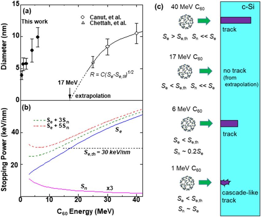
www.nature.com/scientificreports/
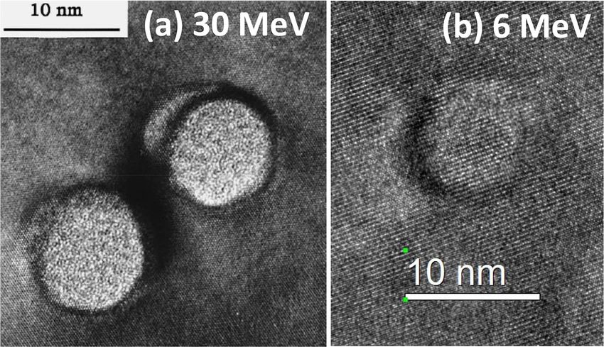
Figure 1. Ion energy dependence of (a) track diameter, (b) electronic (Se), nuclear (Sn), and effective (Seff )
stopping powers (K = 3 and 5). In (a), the open circles, open triangle, and closed circles, respectively, denote
data from Canut et al.4, Chettah et al.7, and the present study. Se,th denotes the threshold Se extrapolated from
the data at 25 MeV and higher. (c) Schematic depiction of the ion energy dependence of track formation and its
relationship to the stopping powers.
energy decreases from 40 MeV, 30 MeV, to 25 MeV, the track mean diameters decreased from 10.5 nm, 8.4 nm,
to 6 nm. An extrapolation suggested that the tracks would no longer be formed at less than 17 MeV7.
In this letter, we report the ion track formation in c-Si induced by C60+ ion irradiation between 1 and 6 MeV,
which are much lower than the above-mentioned threshold of 17 MeV. Surprisingly, large tracks of ~ 10 nm in
diameter were formed with 6 MeV irradiation, which are comparable in size to those with 40 MeV irradiation.
Furthermore, although the sizes decreased, the tracks were observed down to 1 MeV C 60 irradiation or lower.
These observations clearly indicate that the tracks are formed at much lower energy than the threshold of 17 MeV
which was extrapolated from the high energy data, indicating another mechanism for the track formation which
is active under 1–6 MeV C 60 irradiation. Possible candidates are synergy effects between the electronic and the
nuclear energy deposition (Se and Sn)9–12, and the transient boiling-melting transitions with recrystallization.
Results
The open symbols in Fig. 1a show the ion track diameters in c-Si, formed by C60 ion irradiation (E ≥ 25 MeV), as
reported in past literature7,8,13. The energy dependencies of the electronic and nuclear stopping powers, Se and
Sn, of C
60 ions in c-Si are plotted in Fig. 1b, which were approximated as the sum of sixty independent carbon
monomer ions with the energy of (E/60) each, and expressed as,
Si (E, C60 ) = 60Si (E/60, C1 ) (1)
where i = n (nuclear) or e (electronic) . The monomer stopping power Si (E/60, C1) was derived from SRIM
14
201315. At E > 20 MeV, Se is more than 10 times greater than Sn, and the former increases with the energy while
the latter decreases. Canut et al.7 plotted the squared radius of the ion tracks (R2) versus Se, and confirmed the
square root law:
R = C(Se − Se,th )1/2 , (2a)
Scientific Reports | (2021) 11:185 | https://doi.org/10.1038/s41598-020-80360-8 2
Vol:.(1234567890)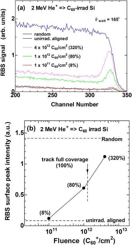
www.nature.com/scientificreports/
Figure 2. Bright-field TEM images of c-Si samples irradiated with (a)–(c) 6 MeV C60+, (d)–(f) 4 MeV C60+,
(g,h) 1 MeV C60+, and (i) 200 MeV X e14+ ions. All the samples were prepared by the pre-thinned configurations,
except (c), (f), and (h) by the post-thinned configurations. Although both 200 MeV X e14+ ions and 4 MeV C60
ions provide almost the same Se in c-Si, tracks were not observed in the former case, as shown in (i). While 4
and 6 MeV C60+ ions exhibit almost straight tracks (c,f), 1 MeV C60+ ions exhibit skewed tracks, which could
indicate crossover from ion tracks to collision cascades.
where Se,th and C denote the threshold stopping of ~ 30 keV/nm and a prefactor constant, respectively. The
square root law (2a) is a phenomenological law and has a following relation with the analytical thermal spike
(ATS) model16: The ATS model gives
R2 = a(0)2 ln Se /Se,th , (3a)
Se < 2.7Se,th ,
R2 = a(0)/2.7Se,th Se . Se > 2.7Se,th (3b)
where Se,th and a(0) denote the threshold Se for the track formation and the initial width of the radial distribution
of temperature in the track, respectively. When (Se / Se,th) = (1 + x), where x ≪ 1, the relation ln (1 + x) ~ x is hold.
Then, ln (Se/Se,th) is approximated by (Se/Se,th – 1), the square root law (2a) is derived:
R2 = a(0)2 (Se − Se,th )/Se,th . (4)
However, because of different Se dependence between the square root law and the ATS, the deviation between
them becomes larger with increasing Se as shown in Fig. S-1 in the supplementary materials.
The validity of the square root law was confirmed by Kamarou, et al. in various semiconductors including
InP, GaAs, Ge, and Si, irradiated with high energy C60 ions17. Following the tradition, the square root law is
applied in this paper.
In the above-cited studies, the stopping power was calculated using, e.g., TRIM 9718. In this study, the previous
stopping power values were recalculated using the latest code SRIM 201315. The Se,th of 30 keV/nm is extrapolated
using SRIM 2013. However, different values of Se,th of 37 keV/nm17 and 32 keV/nm7 were calculated from the
same experimental data using various TRIM codes.
As shown in Fig. 1a, the fitting by Eq. (2a) well matched the data points. Note that the abscissa is not plotted
with Se but with the energy. Following the extrapolation, the track radius becomes null at ~ 17 MeV7; that is, no
tracks were formed below ~ 17 MeV. While the square root law (2a) could be a rough approximation, the exist-
ence of the Se threshold is a typical behavior of latent ion tracks formed in materials by SHI irradiation, which
odel19.
is ascribed to the melting heat in the inelastic thermal spike (i-TS) m
Figure 1a shows that ion tracks of ~ 10 nm in diameter were observed under 6 MeV C60 irradiation, far below
the hitherto-reported threshold of ~ 17 MeV7 (hereafter termed the ‘electronic threshold’). It should be noted
that the track diameters at 6 MeV were comparable to those at 40 MeV, and larger than those at 30 MeV. These
Scientific Reports | (2021) 11:185 | https://doi.org/10.1038/s41598-020-80360-8 3
Vol.:(0123456789)www.nature.com/scientificreports/
facts indicate that there is a mechanism for energy deposition not only from Se but probably also from Sn, since
Se monotonously decreased but Sn increased with decreasing energy as shown in Fig. 1b.
Figure 2 shows bright-field transmission electron microscopy (TEM) images of irradiated c-Si samples. As
described in the Methods section, we prepared TEM specimens in two different configurations, i.e., pre-thinned
(planar) and post-thinned (cross-sectional). Figure 2a shows a planar image (i.e., a pre-thinned sample) of c-Si
irradiated with 6 MeV C 60+ ions. Dark dots of ~ 10 nm in diameter are observed. The sample was irradiated with
an incident angle of 7° to avoid channeling. Since cos (7°) ~ 0.993, the deformed circular images of the tracks
could not be due to the non-normal incidence. In all the observed pre-thinned samples, the areal density of the
tracks was in the same order of the magnitude as the ion fluence. Figure 2b shows a 30°-tilted image of the same
sample (in a lower magnification). The nearly circular dots in Fig. 2a turned to cylinders in Fig. 2b, supporting
the fact that the dark regions are ion tracks.
Figure 2c shows a cross-sectional (post-thinned) image of a sample irradiated with 6 MeV C 60+ ions, which
indicates the depth profiles of the ion tracks. The black layer is a deposited Pt layer for a surface marker. Many
tracks were observed but they were almost free from overlaps. The three different configurations of observations
(planar, inclined planar, and cross-section) firmly confirm the formation of the ion tracks. The track lengths
showed some variation with the mean length of 66.3 nm and the standard deviation of 7.9 nm. While many
hillocks were observed in quartz ( SiO2) crystal irradiated with the same c onditions20, the hillocks were not
observed in the case of c-Si.
Furuno et al. reported that the tracks could be formed in low-quality evaporated films of Si under 207 MeV
Au13+ irradiation (Se = 17 keV/nm)21. Since this report21 was inconsistent with other observations in crystalline
Si4,5, the track formation was ascribed to the low-quality (low thermal conductivity, high electron–phonon
coupling, etc.) of the evaporated Si films (probably in an amorphous phase). However, our observation of the
tracks cannot be attributed to bad quality of the samples. Our samples were commercial available crystalline Si.
Possibly, the pre-thinned samples (e.g., Fig. 2a) could be slightly damaged since they were thinned by focused
ion beam (FIB) of 30 keV Ga+ before C60 irradiation. However, the same tracks are also observed in the post-
thinned samples (Fig. 2c), which were not damaged with FIB before C60 irradiation. This fact confirmed that the
damage in the pre-thinned samples were minimum and probably negligible. Furthermore, the track formation
under 1–6 MeV C 60 irradiation, which we observed, is an intrinsic phenomenon, not induced by pre-damage.
Figure 2d–f show the tracks formed by 4 MeV C 60+ ion irradiation. Compared to the tracks formed by 6 MeV
ions, these tracks (4 MeV) were slightly smaller and shorter. Track formation in c-Si was also confirmed with
C60+ ions of 3, 2, and 1 MeV. Figure 2g,h show the track formation with 1 MeV C 60+ ion irradiation, in the pre-
thinned (g) and post-thinned (h) configurations, respectively. With decreasing the ion energy to 1 MeV, both
the diameter and length of the tracks decreased compared to higher energies.
It should be noted that the shapes of the ion tracks formed by 1 MeV ions are not straight as those formed
by higher energies. As well known, the high electronic energy deposition Se forms damage regions of straight
cylinders, while the high nuclear energy deposition Sn forms more random and extended collision cascades. As
shown in Fig. 1b, a 1 MeV C 60 ion has comparable high Se and high Sn. The formed tracks could be skewed tracks
as observed in Fig. 2h, as the consequence of both the contributions of Se and Sn.
Figure 2i shows a pre-thinned sample irradiated with 200 MeV X e14+ ions (Se = 14 keV/nm and Sn = 0.05 keV/
nm); the Se value being comparable to that of the 4 MeV C60 ions (Se = 15 keV/nm and Sn = 3 keV/nm). However,
no tracks were observed in this case, indicating the importance of the non-negligible Sn contribution (i.e., the
synergy effect) for the track formation.
Discussion
The data shown in Fig. 1a, i.e., the energy dependence of the track diameters, were plotted with squared radius
R2 versus the electronic stopping power Se in Fig. 3. The Se was derived from Eq. (1). Both the high energy data
(E ≥ 25 MeV) and the low energy one (E ≤ 6 MeV) are well fitted with the square root laws but different parameter
values, i.e.,
R = Ci (Se − Sie th )1/2 , (i = L or H). (2b)
where the superscripts L and H denote the low and high energy region, respectively. The threshold stoppings were
Se,thL = 4.2 keV/nm and Se,thH = 30 keV/nm for E ≤ 6 MeV and E ≥ 25 MeV, respectively. The high energy threshold
was ten times higher than the low energy one. Particularly, the threshold of 4.2 keV/nm was extraordinarily low.
Itoh et al. have collected the Se thresholds of 43 materials in their paper22. Among the 43 materials, those having
the thresholds less than 4.2 keV/nm (our case at E ≤ 6 MeV) are limited to only four materials: SiO2 (2 keV/nm),
a-Ge (3 keV/nm), LiF (4 keV/nm), and BaFe12O19 (4 keV/nm)22. Since c-Si is known to have very high threshold,
something unusual could happen under the C60 ion irradiation at E ≤ 6 MeV.
Contrary, the prefactor for the low energy (CL = 1.28 nm3/2/keV1/2 for E ≤ 6 MeV) and that for the high energy
(CH = 1.17 nm3/2/keV1/2 for E ≥ 25 MeV) are almost the same, irrespective of much different energy regions.
According to the i-TS model, the threshold Se,th relates to the heat for the melting. The similar values of the pref-
actor C for high and low energy regions indicate that the track radius increases in almost the same manner with
the additional Se, i.e., (Se – Se,th), irrespective of Se,th. Almost the same value of CL and CH could be a reasonable
consequence, because the material is the same, i.e., c-Si. On the other hand, the large difference in the threshold
Se,th indicates that the melting (or the boiling) is induced with very low value of Se in the low energy region,
where Sn is not negligible. Therefore, there must be an additional heat source except Se. The strongly reduced
threshold could be ascribed to much more efficient heat source rather than the Se but probably Sn. For reference,
a data point of 200 MeV Xe ion is also shown in Fig. 3, which has similar Se with 4 meV C60 ion but much lower
Sn. Clearly the tracks are not formed under 200 MeV Xe irradiation.
Scientific Reports | (2021) 11:185 | https://doi.org/10.1038/s41598-020-80360-8 4
Vol:.(1234567890)www.nature.com/scientificreports/
Figure 3. The energy dependence data of the track radii shown in Fig. 1a were plotted with the squared radius
R2 versus electronic stopping power Se. The solid liens indicate the square root laws as shown by Eq. (2b). The
high (open circles) and low (closed circles) energy data fall on the same law with different parameters. The
thresholds and the prefactors fitted at high and low energy regions were denoted by Se,thH, CH, and Se,thL, CL,
respectively. A data point of 200 MeV Xe ion is also indicated.
Since the tracks formed by the high energy (E ≥ 25 MeV) are ascribed to the electronic energy deposition, one
might consider that the tracks by the low energy (E ≤ 6 MeV) could be formed by the purely nuclear energy depo-
sition, e.g., the collision cascades. However, the low energy tracks (E ≤ 6 MeV) also depend on Se via the square
root law as shown in Fig. 3, indicating that Se plays an important role even in the low energy region (E ≤ 6 MeV).
Figure 4a shows the track lengths determined from the post-thinned samples by closed circles. Here we need
to recall the definition of two quantities: Ion range (projected range) is the depth where implanted ion terminates,
while the track length is the length of the modified region formed by an ion. Even beyond the track length, the
ion goes further without forming track. The ion range is longer than the track length. The track termination of
swift monomer ion is induced when the Se of the ion decreases below the threshold. Contrary, in the case of C60
ions, there is another channel for the track termination, i.e., the fragmentation of the C 60 ions8. Also there are
two mechanisms for the fragmentation: (i) Coulomb repulsion between ionized carbon atoms constituting a C 60
molecule8 and (ii) collisions of carbon atoms constituting a C60 molecule with Si matrix8. Dunlop et al. concluded
that the latter (C-Si collisions) are the dominant process for the fragmentation of 30 MeV C 60 ion irradiation8.
Since the latter process become more dominant for lower energy, the fragmentation processes in our experiments
(E = 1–6 MeV) are mostly governed by the C 60-Si collisions.
60 molecule is assumed as 60 independent single C ions with the same energies of E/60, the ion range RP
If a C
of a C
60 ion can be approximated by the ion range of the single C ion with the same velocity, i.e.,
RP (E, C60 ) = RP (E/60, C1 ). (5)
The right-hand side of the Eq. (5), RP (E/60, C1), i.e., the projected range of single carbon ion in c-Si with the
energy of E/60, was calculated by SRIM 201315. The calculated ion ranges were plotted in Fig. 4a, which were
much longer than the ion tracks observed by TEM.
Figure 4b shows the depth profiles of the electronic energy deposition Se induced by a C 60 ion, which were
calculated by Eq. (1). The track lengths are indicated by rectangles with error bars. The incident Se values of 6 MeV
C60 ion at the surface of c-Si is 18.4 keV/nm, which decreases to 18.2 keV/nm at the depth of 66 nm where the
track terminated. The incident Se value of 4 MeV C 60 at the surface is 16.3 keV/nm, which is much lower than the
Se value at the end of the track of 6 MeV C60 ion (18.2 keV/nm). Even though, tracks of 57 nm long in average
are formed under 4 MeV C60 irradiation. In the case of 1 MeV C60 irradiation, the incident Se at the surface is
8.5 keV/nm, which is less than a half of the Se value at the end of the 6 MeV C60 track (18.2 keV/nm). However,
tracks of 33 nm long in average are formed. From these observations, it is concluded that the termination of the
tracks is not induced when the Se value becomes below the threshold value but probably when the fragmentation
of the C 60 cluster is induced. When a C 60 ion is divided into N fragments, each fragment has Se/N in average,
which results in drastic reduction of the Se.
Figure 5 exhibits high-resolution (HR) planar TEM images of ion tracks in c-Si irradiated with C60 ions of (a)
30 MeV8 and (b) 6 MeV. While a nearly circular track was observed in Fig. 5b, a striking observation was that the
track region also exhibited lattice fringes, coincided with the unirradiated region, i.e., a defective crystalline track.
Scientific Reports | (2021) 11:185 | https://doi.org/10.1038/s41598-020-80360-8 5
Vol.:(0123456789)www.nature.com/scientificreports/
Figure 4. (a) Ion energy dependence of the track length of C60 ions in c-Si is shown by closed circles. The line
is the ion range estimated from the Eq. (5). (b) Depth dependence of the electronic energy loss Se for E = 1, 3, 4,
and 6 MeV, calculated by Eq. (1) using SRIM 201315 (www.srim.org). The track lengths observed by XTEM are
shown by rectangles with error bars.
Dunlop et al. observed amorphous tracks in c-Si irradiated with 30 MeV C 60 irradiation as shown in Fig. 5a.8
While we have also carried out HR-TEM observations of tracks formed by 4 MeV C 60 ions (not shown) in addi-
tion to 6 MeV one, they also showed similar defective crystalline tracks.
Dunlop et al. observed that recrystallization of ion tracks in c-Si during the HR-TEM observation8. Since they
irradiated c-Si with 30 MeV C60 ions, the samples could be much more damaged than our samples irradiated
with 6 MeV C60 ions. Much quicker recrystallization could be induced in our cases.
Another possibility is due to much shorter length of our tracks: The mean track length was 66.3 nm for
6 MeV C60 ions, which is thinner than the TEM sample (~ 100 nm thick). Since the tracks terminate inside the
TEM samples, the remaining crystalline parts deeper than the track-length would contribute for the fringes.
However, the HR-TEM images are so clear that this explanation seems less plausible. Up to now, a lot of studies
Scientific Reports | (2021) 11:185 | https://doi.org/10.1038/s41598-020-80360-8 6
Vol:.(1234567890)www.nature.com/scientificreports/
Figure 5. High resolution TEM images of ion tracks in c-Si irradiated with C
60+ ions of (a) 30 MeV (
reproduced with permission from A. Dunlop et al. Ref.8) and of (b) 6 MeV (this work).
have been carried out to discover ion tracks in c-Si using S HIs4,5. However, there are no reports on defective
crystalline tracks in c-Si.
To confirm the defective crystalline tracks, Rutherford backscattering spectrometry and channeling (RBS/C)
measurements were carried out. Figure 6a exhibits RBS/C spectra of random and aligned configurations of an
unirradiated sample, and of the aligned configurations of the samples irradiated with 6 MeV C60+ ions at three
different fluences. With increasing the fluence, the surface peak around 330 channel, which is due to the scatter-
ing by the tracks, increased but does not reached at the random level. The numbers in parentheses indicate the
track coverage ratio (TCR) at the surface, which is defined as
TCR = πR2 � (6)
where R and Φ denote the mean radius of the ion track and the C 60 fluence, respectively.
The intensity of the surface peak was plotted with the fluence in Fig. 6b. From the track radius shown in
Fig. 1a, TCR reaches at 100% at the fluence of 1.3 × 10¹² C60/cm2, where almost all the surface of the sample is
covered by the tracks. If the tracks could be amorphous, the surface peak intensity would reach the random level
and would saturate at TCR ~ 100%. However, the experiments showed that the surface peak intensity reached
at only ~ 46% of the random level at TCR of 100% and that the intensity monotonically increased even beyond
the TCR of 100%. It should be noted that even ~ 46% of the random level could indicate significant disorder,
defects or possibly partial amorphization. However, HR-TEM image (Fig. 5b) does not show any evidence of
partial amorphization.
Furthermore, the surface peak increased to the fluence to 4 × 10¹² C60/cm2 (TCR = 320%), where the multiple
overlaps of the tracks are expected. Even though, the surface peak intensity did not reach at the random level of
the RBS/C measurements. Consequently, these observations support the formation of defective crystalline ion
tracks, rather than amorphous ones, under 6 MeV C 60 ion irradiation.
At the beginning, we considered that the tracks observed in Fig. 5b were originally amorphous but crystallized
by electron beam irradiation under HR-TEM observation. However, the samples used for the RBS/C measure-
ments were not irradiated by electron beam but only 2 MeV He+ ions. Consequently, the crystallinity of the ion
tracks has been confirmed by two different methods, i.e., HR-TEM and RBS/C, which further supports that the
defective crystalline tracks in c-Si are not a consequence of improper experimental procedures but an intrinsic
nature of this system.
Szenes and T oth23 irradiated yttrium-iron-garnet (YIG) Y 3Fe5O12 with C 60 ions of 3.5, 5, and 7 MeV, and
observed the ion track formation. To evaluate the synergy effect of Se and Sn on track formation, they applied an
effective stopping power defined by
Seff = Se + K Sn , (7)
with a coefficient K of 2.2 for the YIG. Kitayama et al. irradiated amorphous SiN films with 540 keV C602+
24
ions, and evaluated the synergy effect on the electronic and collisional sputtering. To explain the data, they used
K = 2.5. We have adopted this formalism. As shown in Fig. 1b, even assuming K = 3, Seff is less than the electronic
threshold of 30 keV/nm at 6 MeV. If K = 5 is assumed, Seff becomes greater than the threshold of 30 keV/nm at
6 MeV, i.e., the track formation is approved. In this case, however, Seff at 1 MeV is higher than at 6 MeV, which is
Scientific Reports | (2021) 11:185 | https://doi.org/10.1038/s41598-020-80360-8 7
Vol.:(0123456789)www.nature.com/scientificreports/
Figure 6. (a) RBS/C spectra of c-Si in unirradiated state and irradiated with 6 MeV C 60+ ions to three different
fluences. (b) Fluence dependence of the surface peak around 330 channel. Horizontal broken lines indicate the
random and aligned levels in unirradiated sample. Numbers in parentheses indicate the track coverage ratio at
the fluences, which is defined by eq. (6). The vertical broken line indicates the track full coverage, i.e., 100%.
inconsistent with the larger track diameters at 6 MeV than those at 1 MeV. This is because Eq. (7) is an empirical
rule, which holds in limited energy region only. If it would hold also in very low energy where Se 1. A transition
from 6 to 1 MeV could happen because the track shapes at 6 MeV are nearly straight (Fig. 2c) but those at 1 MeV
are skewed cylinder shapes (Fig. 2h). Different spatial distributions of Se (straight cylinders) and Sn (skewed
cylinder) could reduce the synergy effect efficiency, which has already been reported in z ircon25.
While the mechanism of the track formation at 1–6 MeV is still an open question, we suggest two issues: (i)
As pointed by Weber et al.9, the track radii became larger in pre-damaged samples. For C 60 ions of 1–6 MeV, Sn
is not negligible to Se. The damage formed by Sn assists the track formation by Se. Since the fluence is low, the
track formation by Se assisted by Sn is induced by the same ion. This is not the pre-damage effect but the “in-
situ” damage effect. Another issue is that Chettah et al.13 proposed the boiling transition for the track formation
at 30–40 MeV C60 ions from the analysis of the inelastic thermal spike model. We speculate that the tracks by
Scientific Reports | (2021) 11:185 | https://doi.org/10.1038/s41598-020-80360-8 8
Vol:.(1234567890)www.nature.com/scientificreports/
the melting transition could not been observed because of the perfect recrystallization under SHI irradiation
where Sn is negligible. We attribute the track formation under 30-40 MeV C60 irradiation to the boiling transi-
tion. Contrary, non-negligible Sn under 1–6 MeV C60 irradiation prevents the perfect recrystallization at the
melting transition, which results in the track formation by the melting transition.
Summary
The ion energy dependence of track formation in c-Si, and the relevant stopping powers, are schematically sum-
marized in Fig. 1c. The C60 irradiation higher than 25 MeV, Sn is much less than Se. Consequently the synergy
effect is not expected (i.e., Se > Se,th > > Sn). The damage formation is governed only by Se. When Se decreases below
the threshold, i.e., Se < Se,th, tracks are expected to be no longer formed. (This is only due to the extrapolation).
However, a further decrease in the energy results in an increase in Sn, activating the synergy effect: Tracks are
formed once again at 1–6 MeV. With further decreasing energy, the contribution of Sn increases further, finally
resulting in cascade-like tracks being observed at 1 MeV.
While the Se,th determined from the square root law at E ≥ 25 MeV was reasonably high as 30 keV/nm, the
Se,th at E ≤ 6 MeV was 4.2 keV/nm, which is extraordinarily low and inconsistent with the fact that c-Si is insensi-
tive to SHIs. There must be another heat source other than Se, but probably Sn for C60 irradiations at E ≤ 6 MeV.
However, it should be noted that the track diameters at low energy (E ≤ 6 MeV) depend on Se via the square root
law. It seems that the Se plays an important role in the track formation also at low energy (E ≤ 6 MeV). Purely
nuclear origin, such as the collision cascades are excluded, while it does not mean to exclude the synergy effects
between Se and Sn. The track length is determined not by a decrease of Se, but by the fragmentation of C 60 mol-
ecules. Another scenario is that the track formations at 6 MeV and those at 30 MeV could be ascribed to the
melting and boiling transitions, respectively. Whilst the tracks by the melting transition are fully recrystallized
under SHI irradiations, the recrystallization is hindered due to non-negligible nuclear collision contribution.
Methods
C60 ion irradiation. 60+ ions was conducted at the Takasaki Advanced Radiation Research
The irradiation of C
Institute (TARRI), of the National Institutes for Quantum and Radiological Science and Technology (QST),
using a 3 MV tandem accelerator and a newly developed high-flux C60 negative ion source. The samples were
mostly irradiated to a low fluence of 5 × 10¹⁰ C60/cm2 to avoid overlaps between the tracks. For precise control of
the low fluence, the ion flux was reduced to below 50 pA through an aperture of 3 mm in diameter, while using
the high-flux ion source. The incident angle was set to 7° to avoid any channeling effect. Since cos (7°) = 0.993,
beams deviating from the normal incidence did not significantly modify the shapes of the tracks. For compari-
son, some samples were irradiated with 200 MeV X e14+ ions from the tandem accelerator in the Japan Atomic
energy Agency (JAEA), Tokai Research and Development Center.
Sample preparation. Silicon samples were cut from commercially available Si wafers of p-type conduc-
tion (boron-doped), with resistivity of ~ 1 Ωcm, surface orientation of < 1 1 1 > , and thickness of ~ 0.38 mm. The
samples were mechanically cut into 3 mm × 4 mm rectangles, which are hereafter called bulk samples. The bulk
samples were immersed in hydrofluoric acid to remove the surface oxide.
Two different TEM specimens (pre-thinned and post-thinned) were prepared from the bulk samples. In
the case of the post-thinned samples, a group of bulk samples were irradiated by a C 60+ beam with an incident
angle of 7° to the 3 mm × 4 mm faces, and the TEM specimens were milled down to a thickness of ~ 100 nm to
observe the depth profile of the ion tracks. The TEM specimens were fabricated with 30 keV Ga focused ion
beam (FIB) milling. To identify the surface position in the cross-sectional configuration, a thin layer of Pt was
deposited on the sample surface before the FIB milling. The other bulk samples (pre-thinned) were first milled
down to a thickness of ~ 100 nm, and then irradiated with C 60+ ions with an incident angle of 7° to observe the
track faces. See Fig. S-2 for details.
TEM observation. TEM observation of both configurations (i.e., the depth and planar profiles) was con-
ducted using a JEOL JEM-2100 microscope (with a LaB6 thermal emission e-gun). HRTEM observation was
carried out using JEOL JEM-2100F microscope (with a Schottky-type field emission e-gun). Both the accelera-
tion voltages were 200 kV. According to past literature, the tracks in c-Si were recrystallized with prolonged TEM
observation. Careful observations were performed to minimize the electron beam current and TEM observation
time.
Rutherford backscattering spectrometry and channeling (RBS/C) measurements. He+ ions of
2 MeV from a single-end accelerator in QST-Takasaki were used. The beam size was 1 mm in diameter and the
scattering angle was 165°. Scattered ions were monitored by a surface-barrier detector, with the accumulated
charge of 10 μC for a spectrum.
Data availability
The datasets and materials generated during the current study are available from the corresponding author on
reasonable request.
Received: 14 March 2020; Accepted: 15 December 2020
Scientific Reports | (2021) 11:185 | https://doi.org/10.1038/s41598-020-80360-8 9
Vol.:(0123456789)www.nature.com/scientificreports/
References
1. Avasthi, D. K. & Mehta, G. K. Swift Heavy Ions for Materials Engineering and Nanostructuring; https://doi.org/10.1007/978-94-
007-1229-4 (Springer, 2011).
2. Amekura, H., Chen, F. & Jia, Y. Shape elongation of nanoparticles induced by swift heavy ion irradiation. In Ion Irradiation of
Dielectrics for Photonic Applications Chap. 5, https://doi.org/10.1007/978-981-15-4607-5_5 (Springer Nature, 2020).
3. Young, D. A. Etching of radiation damage in lithium fluoride. Nature 182, 375–377. https://doi.org/10.1038/182375a0 (1958).
4. Mary, P., Bogdanski, P., Toulemonde, M., Spohr, R. & Vetter, J. Deep-level transient spectroscopy studies of U-irradiated silicon.
Nucl. Instrum. Methods Phys. Res. Sect. B Beam Interactions Mater. Atoms 62, 391–393. https: //doi.org/10.1016/0168-583X(92)95263
-Q (1992).
5. Toulemonde, M. et al. High Energy Heavy Ion Irradiation of Silicon. physica status solidi a 114, 467–473. Doi: https://doi.
org/10.1002/pssa.2211140205 (1989).
6. Nastasi, M., Mayer, J. & Hirvonen, J. K. Ion-Solid Interactions: Fundamentals and Applications (Cambridge University Press, Cam-
bridge, 1996).
7. Canut, B., Bonardi, N., Ramos, S. M. M. & Della-Negra, S. Latent tracks formation in silicon single crystals irradiated with fuller-
enes in the electronic regime. Nucl. Instrum. Methods Phys. Res. Sect. B Beam Interact. Mater. Atoms 146, 296–301. https://doi.
org/10.1016/S0168-583X(98)00512-6 (1998).
8. Dunlop, A., Jaskierowicz, G. & Della-Negra, S. Latent track formation in silicon irradiated by 30 MeV fullerenes. Nucl. Instrum.
Methods Phys. Res. Sect. B Beam Interact. Mater. Atoms 146, 302–308. https://doi.org/10.1016/S0168-583X(98)00509-6 (1998).
9. Weber, W. J. et al. Synergy of elastic and inelastic energy loss on ion track formation in S rTiO3. Sci. Rep. 5, 7726. https://doi.
org/10.1038/srep07726 (2015).
10. Zarkadoula, E., Pakarinen, O. H., Xue, H., Zhang, Y. & Weber, W. J. Predictive modeling of synergistic effects in nanoscale ion
track formation. Phys. Chem. Chem. Phys. 17, 22538–22542. https://doi.org/10.1039/C5CP02382C (2015).
11. Zarkadoula, E., Jin, K., Zhang, Y. & Weber, W. J. Synergistic effects of nuclear and electronic energy loss in KTaO3 under ion
irradiation. AIP Adv. 7, 015016. https://doi.org/10.1063/1.4973938 (2017).
12. Jin, K., Zhang, Y. & Weber, W. J. Synergistic effects of nuclear and electronic energy deposition on damage production in K TaO3.
Mater. Res. Lett. 6, 531–536. https://doi.org/10.1080/21663831.2018.1495131 (2018).
13. Chettah, A. et al. Behavior of crystalline silicon under huge electronic excitations: a transient thermal spike description. Nucl.
Instrum. Methods Phys. Res. Sect. B Beam Interact. Mater. Atoms 267, 2719–2724. https: //doi.org/10.1016/j.nimb.2009.05.063 (2009).
14. Bouneau, S. et al. Very large gold and silver sputtering yields induced by keV to MeV energy Aun clusters (n = 1–13). Phys. Rev. B
65, 144106. https://doi.org/10.1103/PhysRevB.65.144106 (2002).
15. Ziegler, J. F., Biersack, J. P. & Ziegler, M. D. SRIM - The Stopping and Range of Ions in Matter. www.srim.org (SRIM Co., 2008).
16. Szenes, G. General features of latent track formation in magnetic insulators irradiated with swift heavy ions. Phys. Rev. B 51,
8026–8029. https://doi.org/10.1103/PhysRevB.51.8026 (1995).
17. Kamarou, A., Wesch, W., Wendler, E., Undisz, A. & Rettenmayr, M. Radiation damage formation in InP, InSb, GaAs, GaP, Ge, and
Si due to fast ions. Phys. Rev. B 78, 054111. https://doi.org/10.1103/PhysRevB.78.054111 (2008).
18. Ziegler, J. F., Biersack, J. P. & Littmark, U. The Stopping and Range of Ions in Solids, Vol. 1 (Pergamon, 1985).
19. Dufour, C. & Toulemonde, M. Models for the description of track formation, in Ion Beam Modification of Solids Vol. 61 (eds Werner
Wesch & Elke Wendler) Ch. 2, 63–104. https://doi.org/10.1007/978-3-319-33561-2 (Springer, 2016).
20. Amekura, H. et al. C60 ions of 1 MeV are slow but elongate nanoparticles like swift heavy ions of hundreds MeV. Sci. Rep. 9, 14980.
https://doi.org/10.1038/s41598-019-49645-5 (2019).
21. Furuno, S., Otsu, H., Hojou, K. & Izui, K. Tracks of high energy heavy ions in solids. Nucl. Instrum. Methods Phys. Res. Sect. B
Beam Interact. Mater. Atoms 107, 223–226. https://doi.org/10.1016/0168-583X(95)00813-6 (1996).
22. Itoh, N., Duffy, D. M., Khakshouri, S. & Stoneham, A. M. Making tracks: electronic excitation roles in forming swift heavy ion
tracks. J. Phys. Condens. Matter 21, 474205. https://doi.org/10.1088/0953-8984/21/47/474205 (2009).
23. Szenes, G. & Toth, L. Basic restrictions for theories of ion-induced track formation: ignored relationships between experimental
data. Phys. Scr. https://doi.org/10.1088/1402-4896/ab300c (2019).
24. Kitayama, T. et al. Sputtering of amorphous SiN induced by 540 keV C 602+ irradiation. Unpublished. (2014).
25. Zarkadoula, E., Toulemonde, M. & Weber, W. J. Additive effects of electronic and nuclear energy losses in irradiation-induced
amorphization of zircon. Appl. Phys. Lett. 107, 261902. https://doi.org/10.1063/1.4939110 (2015).
Acknowledgements
A part of the study was supported by the Inter-organizational Atomic Energy Research Program through an
academic collaborative agreement among JAEA, QST, and the Univ. of Tokyo. The authors are grateful to the
crew of the 3-MV tandem accelerator of QST/Takasaki. HA was supported by JSPS-KAKENHI Grant number
18K04898. TEM observation was performed using the facility of the NIMS TEM Station. The authors thank Prof.
H. Tsuchida and Prof. M. Alex Imai (Kyoto Univ.) for their encouragement.
Authors Contributions
A.C., Y.H., K.Y., K.N., and Y.S. have developed the MeV high-flux C
60 ion beam. R.L. and H.A. prepared samples.
Y.S., A.C., Y.H., S.Y. and K.N conducted C60 ion irradiation. N.I and N.O conducted 200 MeV Xe irradiation.
H.A. conducted TEM observation. S.Y., K.N, and Y.S. carried out RBS/C measurements. M.T. supplied much
information on the past literature and valuable suggestions. All the authors joined in discussion of the results
and contributed to manuscript preparation.
Competing interests
The authors declare no competing interests.
Additional information
Supplementary Information The online version contains supplementary material available at https://doi.
org/10.1038/s41598-020-80360-8.
Correspondence and requests for materials should be addressed to H.A.
Reprints and permissions information is available at www.nature.com/reprints.
Publisher’s note Springer Nature remains neutral with regard to jurisdictional claims in published maps and
institutional affiliations.
Scientific Reports | (2021) 11:185 | https://doi.org/10.1038/s41598-020-80360-8 10
Vol:.(1234567890)www.nature.com/scientificreports/
Open Access This article is licensed under a Creative Commons Attribution 4.0 International
License, which permits use, sharing, adaptation, distribution and reproduction in any medium or
format, as long as you give appropriate credit to the original author(s) and the source, provide a link to the
Creative Commons licence, and indicate if changes were made. The images or other third party material in this
article are included in the article’s Creative Commons licence, unless indicated otherwise in a credit line to the
material. If material is not included in the article’s Creative Commons licence and your intended use is not
permitted by statutory regulation or exceeds the permitted use, you will need to obtain permission directly from
the copyright holder. To view a copy of this licence, visit http://creativecommons.org/licenses/by/4.0/.
© The Author(s) 2021
Scientific Reports | (2021) 11:185 | https://doi.org/10.1038/s41598-020-80360-8 11
Vol.:(0123456789)You can also read