Nanotech Cluster and Industry Landscape in Japan - Author: Andrej Žagar Minerva Research Fellow October 2014
←
→
Page content transcription
If your browser does not render page correctly, please read the page content below
Nanotech Cluster and Industry
    Landscape in Japan

                          Author: Andrej Žagar
                       Minerva Research Fellow
                                 October 2014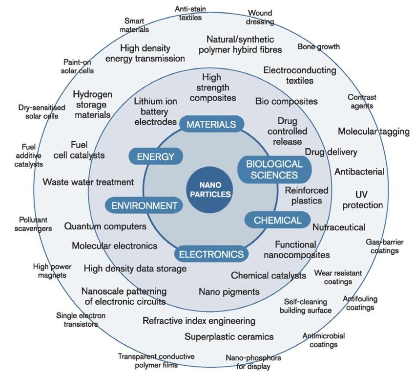
Japanese Nanotech Cluster and Industry Landscape

Table of Contents

List of Abbreviations.................................................................................................................................4

List of figures and tables ..........................................................................................................................5

Acknowledgment .....................................................................................................................................6

1. Nanotechnology ...................................................................................................................................7
1.1 INTRODUCTION ...............................................................................................................................................7
1.2 METHODOLOGY ...............................................................................................................................................8
1.3 NANOTECHNOLOGY APPLICATIONS ...............................................................................................................8
1.4 TRENDS IN NANOTECHNOLOGIES...................................................................................................................9
1.5 FUTURE OF NANOTECHNOLOGY IN JAPAN .................................................................................................. 10

2. Government ...................................................................................................................................... 11
2.1 JAPANESE GOVERNMENT ACTIVITIES ON NANOTECHNOLOGY ................................................................... 11
2.2 GOVERNMENT INVESTMENTS IN NANOTECHNOLOGY ................................................................................ 11
2.3 NANOTECH CLUSTERS IN JAPAN.................................................................................................................. 13

3. Government bodies active in Japanese nanotechnology ................................................................. 14
3.1 CABINET OFFICE, GOVERNMENT OF JAPAN ........................................................................................... 14
3.2 METI ............................................................................................................................................................ 14
3.3 MEXT ........................................................................................................................................................... 14
3.4 NEDO ........................................................................................................................................................... 14
3.5 JETRO .......................................................................................................................................................... 14

4. Nanotechnology platforms in Japan ................................................................................................. 16
4.1 NBCI ............................................................................................................................................................. 16
4.2 NANOTECHNOLOGY EVENTS ........................................................................................................................ 16
4.2.1 NANO TECH EXPO ..................................................................................................................................................... 16
4.2.2 NANOMICRO BIZ ........................................................................................................................................................ 17
4.3 NANOTECH CLUSTER SUPPORT MISSION TO JAPAN – EU-JAPAN CENTRE .............................................. 17

5. Research & development activity ..................................................................................................... 18
5.1 TIA - NANO .................................................................................................................................................. 18
5.2 SUPER CLEAN ROOM (SCR) ........................................................................................................................ 18
5.3 NIMS ............................................................................................................................................................ 18
5.4 AIST ............................................................................................................................................................. 18
5.5 BIO-NANO ELECTRONICS RESEARCH CENTRE ........................................................................................... 19
5.6 NANOTECHNOLOGY PLATFORM JAPAN ....................................................................................................... 19
5.7 NANOFABRICATION PLATFORM .................................................................................................................. 20
5.8 UNIVERSITIES ............................................................................................................................................... 21

6. Nanotech companies in Japan .......................................................................................................... 22
6.1 CASE STUDIES: ............................................................................................................................................. 22
6.1.1 SHOWA DENKO (JAPAN).......................................................................................................................................... 22
6.1.2 GENELITE + GL MATERIALS (JAPAN) ................................................................................................................... 22
6.1.3 OXFORD INSTRUMENTS (UNITED KINGDOM, EU) .............................................................................................. 22
6.1.4 CARBODEON (FINLAND, EU) .................................................................................................................................. 23
6.1.5 GRAPHENEA (SPAIN, EU) ....................................................................................................................................... 23

                                                                                      2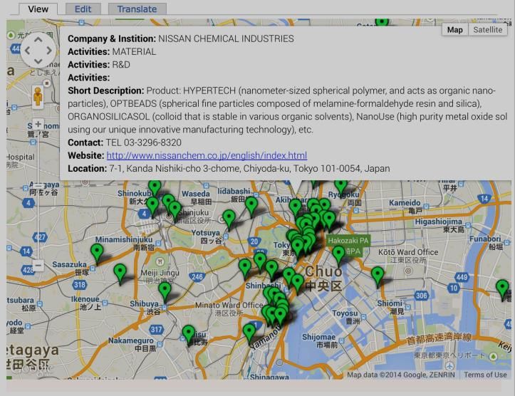
Japanese Nanotech Cluster and Industry Landscape

7. Nanotech industry landscape ............................................................................................................ 24
7.1 NANOTECH INDUSTRY LANDSCAPE MAP ..................................................................................................... 24
7.2 NANOTECHNOLOGY INDUSTRY LANDSCAPE ............................................................................................... 25
7.3 NANOTECHNOLOGY INDUSTRY LANDSCAPE GRAPHIC DISPLAY ................................................................ 26

8. Nanotechnology in European Union and supporting programs ....................................................... 27
8.1 HORIZON 2020 ........................................................................................................................................... 27
8.2 KEY ENABLING TECHNOLOGY – NANOTECHNOLOGY ................................................................................. 27
8.3 JEUPISTE .................................................................................................................................................... 28
8.4 HORIZON 2020 - NATIONAL CONTACT POINT JAPAN .............................................................................. 28
8.5 ENTERPRISE EUROPE NETWORK (EEN) ................................................................................................... 28

9. Business opportunities ...................................................................................................................... 29
9.1 ENTERING THE JAPANESE NANOTECH MARKET ......................................................................................... 30

10. Conclusions and Recommendations ............................................................................................... 31

11. ANNEX ............................................................................................................................................. 33

                                                                                3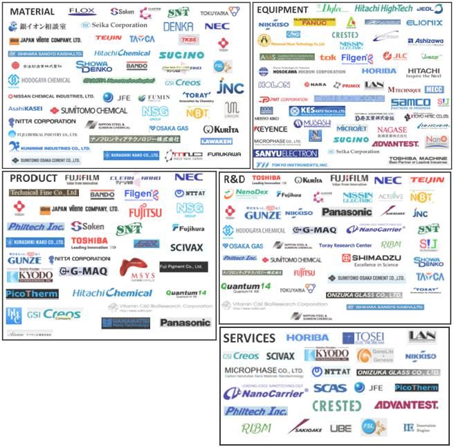
Japanese Nanotech Cluster and Industry Landscape

List of Abbreviations
AFM            Atomic force microscopy
Ag             Silver
AIST           National Institute of Advanced Industrial Science and Technology
ALD            Atomic Layer Deposition
Au             Gold
B2B            Business to business
CAO            Cabinet office
CLUSTER        geographic concentration of interconnected businesses
CNTs           Carbon nanotubes
CVD            Chemical vapor deposition
DDS            Drug deposition system
EEN            Enterprise Europe Network
ESH            Environment, safety & health
EU             European Union
Expo           Exhibition
FIB-SEM        Focused Ion Beam Scanning Electron Microscope
Horizon 2020   Framework program for Research and Innovation
ICT            Information and communication technology
JETRO          Japan External Trade Organization
JEUPISTE       Japan-EU Partnership in Innovation, Science and Technology
KEIDANREN      Japan Business Federation
KEK            High Energy Accelerator Research Organization
KET            Key Enabling Technologies
METI           Ministry of Economy, Trade and Industry, Japan
MEXT           Ministry of Education, Culture, Sports, Science and Technology
N-MEMS         Nano – micro electromechanical systems
NBCI           Nanotechnology Business Creation Initiative
NCP            National contact point for Horizon 2020
NEDO           New Energy and Industrial Technology Development Organization
NIMS           National Institute for Materials Science
NM             Nanometer (10-9 meter)
OEM            Original equipment manufacturer
PVD            Physical vapor deposition
R&D            Research and development
RIT            Regional Industry Tie-up program
SCR            Super Clean Room
SDK            Showa Denko
SEM            Scanning electron microscope
Si             Silicon
SiC            Silicon Carbide
SME            Small and Medium-sized Enterprise
SPM            Scanning probe microscopy
STBP           Science and Technology Basic Plan
STEM           Scanning transmission electron microscope
STI            Science, Technology and Innovation
TIA            Tsukuba Innovation Area

                                             4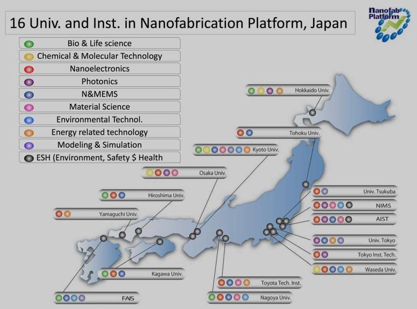
Japanese Nanotech Cluster and Industry Landscape

TiO2                  Titanium dioxide
VC                    Venture Capital
XRF                   X-ray fluorescence
ZnO                   Zinc oxide

List of figures and tables
Figure 1: Nano particles applications, ......................................................................................................8

Figure 2: Nanotechnology patents ...........................................................................................................9

Figure 3: Nanotechnology patents, by applications.................................................................................9

Table 1: Science and technology budget (2006 - 2012) ........................................................................ 12

Figure 4: Science and technology budget ............................................................................................. 12

Table 2: Science and technology budget frame (2012)......................................................................... 13

Figure 5: Share of investments in Science and Technology in Japan, ................................................... 13

Figure 6: Nanotechnology platform Japan, Source: NanotechJapan .................................................... 19

Figure 7: Nanofabrication Platform Japan, ........................................................................................... 20

Table 3: Equipment and technical personnel prices, ............................................................................ 21

Figure 8: Major Universities with activities in nanotechnology ............................................................ 21

Figure 6: Map of nanotech companies in Japan ................................................................................... 24

Figure 7: View of nanotech companies in Tokyo area .......................................................................... 24

Figure 8: Nanotech interactive map with company details. ................................................................. 25

Figure 9: Nanotechnology business landscape in Japan ....................................................................... 26

                                                                      5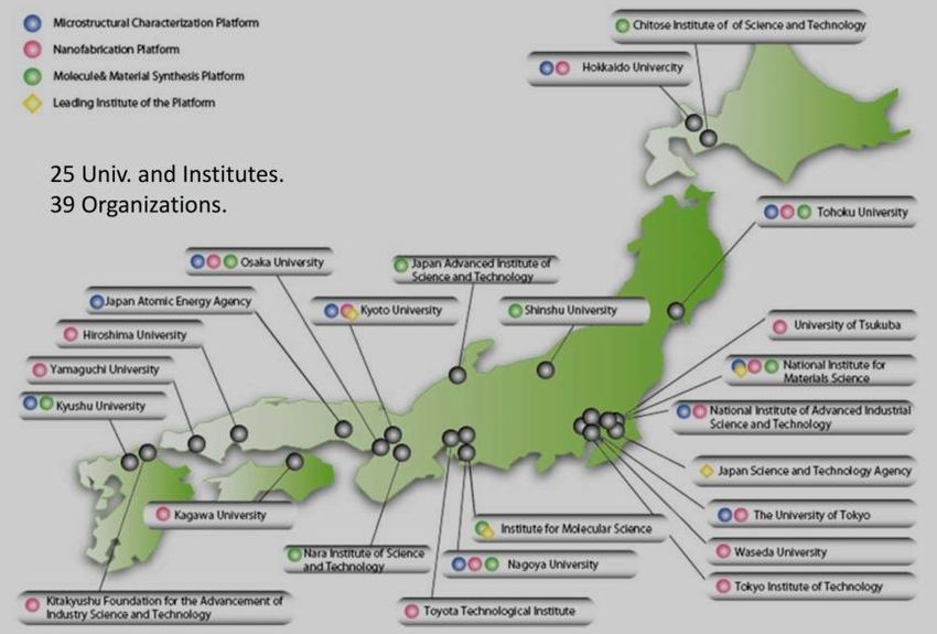
Japanese Nanotech Cluster and Industry Landscape

Acknowledgment
The author wishes to thank Dr. Silviu Jora, General Manager (EU side) of the EU-Japan
Centre for Industrial Cooperation, the staff of the EU-Japan Centre for Industrial
Cooperation and everyone who has kindly offered their time for interviews and their
input.

                                           6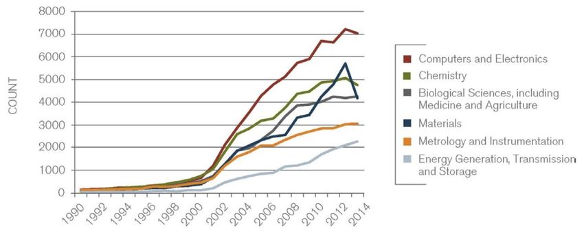
Japanese Nanotech Cluster and Industry Landscape

1. Nanotechnology
1.1 Introduction
Nanotechnology is a technology of producing very small “things”, which are particularly
less than 100 nm in size. One nanometer is 10-9 meters or about three atoms wide and
for comparison, a human hair is about 60-80,000 nanometers wide. Nanotechnology has
the potential to change every part of our lives, and will greatly impact us in the coming
decade. The technology affects all materials (ceramics, metals, polymers, biomaterials,
etc.), which are the foundation of major technological advances.

Traditionally, Japan has been very active in the field of nanotechnology. In the 14th
century the golden pavilion in Kyoto was built, later on when it was coated with gold
leaf, the thickness of the coating was 100 nanometers1. Although that technique is not
used anymore, it exemplifies that the Japanese are historically innovative and precise
engineers. Japan has been among the top three countries in patents and publications in
the field of nanotechnology, although lately Asian countries such as China and Korea are
gaining the momentum surpassing Japan in many fields.

Market size of the Japanese nanotech sector has ranged 29,6 billion euros in 2010 and is
projected to grow extensively in the future reaching 94,4 billion euros in 2020 and
should be worth 188,9 billion euros in 20302.

Japan has produced some important innovations and developments in the field of
nanotechnology; invention of carbon nanotubes has had a great impact on the area and
it has been the foundation for diverse directions of development. Advancements in
Silicon carbide lead to effective semiconductors bringing smaller computer devices with
greater performances. Further developments have been done on Gallium arsenide used
also for thin films in solar cells and detectors; all those achievements can bring new
niches or major markets to Japanese companies.

Despite the economic difficulties that Japan is tackling with, advanced technologies have
always been the driving force of new opportunities and further development. Constant
research and development on new technologies namely nanotechnology can bring
market advantage for innovative companies.

This report aims to provide an overview of the Japanese nanotech sector, its structure
and an industry landscape. The author has had a European and business oriented
perspective on Japan, therefore this report is perhaps more suitable for European
nanotechnology companies potentially planning to enter the Japanese market. One can
get the understanding of the structure of the nanotechnology sector in Japan, as well as
the key government and research bodies, clusters, pointing out how to enter the market,
etc. In the last part of the report one can find the nanotechnology industry landscape and
in the annexes a broad database of Japanese companies that have activities in
nanotechnology.

1   Wikipedia: Kinkaku-ji, Golden pavilion. http://en.wikipedia.org/wiki/Kinkaku-ji
2   Market size estimations by METI

                                                                        7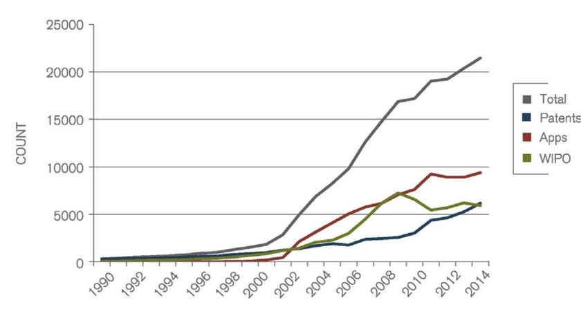
Japanese Nanotech Cluster and Industry Landscape

Additionally to the report, the author has made an interactive map displaying
nanotechnology companies across Japan; their details, contacts and activities. This map
can be found on the website of EU-Japan Centre for Industrial Cooperation –
http://www.eu-japan.eu/interactive-map-nanotech-cluster-and-industry-landscape-
japan

1.2 Methodology
Main points which the report is thriving to are: Who are the key players in the Japanese
nanotech sector, clusters, research and major companies involved in this area? How can
an EU nanotech company enter the market? What kinds of companies are present in this
field?

Data was collected through literature review and interviews with experts from Japanese
government and related organisations, nanotech clusters, research and development
institutes, Japanese and EU nanotechnology companies.

To provide a clear view of the nanotech sector a review of 150 nanotechnology related
companies have been made, that is found in the annex.

1.3 Nanotechnology applications
Nanotechnology has a wide area of applications. Numerous new applications are being
developed across the globe. The diagram bellow shows commercial applications of
inorganic nanoparticles, focus of research and development as well as future directions
is comprehensively displayed.

Figure 1: Nano particles applications,
Source: McDermott, Will & Emery, 2013 Nanotechnology Patent Literature Review

                                                                8
Japanese Nanotech Cluster and Industry Landscape
1.4 Trends in Nanotechnologies
Patent trends shows that nanotechnology has been growing exponentially since the
2000s. At that time, technology has matured and first nanotechnology products rolled
out such as coatings, nanoparticles, nanostructured metals, polymers, etc. Up to 2005,
new active nanostructures were developed: 3d transistors, target drugs, actuators,
adaptive structures, etc., giving new grounds for further development, that is evident in
the shown graphs.
Figure 2: Nanotechnology patents
Source: McDermott, Will & Emery, 2013 Nanotechnology Patent Literature Review
With development of new electronic devices using semiconductors and other nanotech
elements, the most emphasis has been put on computers and electronics followed by
materials and chemistry patents.
Figure 3: Nanotechnology patents, by applications.
Source: McDermott, Will & Emery, 2013 Nanotechnology Patent Literature Review
9Japanese Nanotech Cluster and Industry Landscape
1.5 Future of nanotechnology in Japan
Future advances could change approaches to manufacturing, electronics, IT,
communications, energy and medicine.
Japan priorities for further development of nanotechnology is divided in three pillars:
Green innovation, Life innovation, Recovery and reconstruction from the disaster. Total
budget for this plan that includes nanotechnology is 25 trillion yen (179 billion euro) for
the next 5 years.
Key decision makers in Japan have tailored a strategic program for nanotechnology;
named Cross-ministerial strategic innovation promotion program (SIP)3 has selected
future priority policy issues segmented to:
Energy
- Next-generation power electronics
- Innovative combustion technology
- Innovative structural materials
- Energy carriers
- Next-generation ocean resources development technologies
Next-generation infrastructures
- Technologies for avoidance of accidents and alleviating congestion
- Low-cost operation & maintenance system and long life materials for infrastructure
- Natural disaster forecasts and prediction
Local resources
- Advanced IT (Quantum computing)
- Additive manufacturing
3Presentation: Overview of Materials Science and Nanotechnology R&D in Japan - MEXT (Material Science and Nanotechnology
Development Division, Research Promotion Bureau), May 29, 2014, Kobe University
10Japanese Nanotech Cluster and Industry Landscape
2. Government
2.1 Japanese government activities on nanotechnology
Years of investments into nanotechnology have made Japan amongst the leading
countries in this field. Nanotechnology becoming a national priority technology has
brought immense investments into research and development as well as the research
infrastructure. Cabinet office of Japan, MEXT and METI has recognized the necessity and
has dedicated divisions in the ministries focused only on nanotechnology. Strategic
technology roadmap4 has been produced to outline priorities in future technological
development.
In 2001 the government started its 2nd Science and Technology Basic Plan 5 (STBP)
where nanotechnology and nanomaterials have been prioritized as one of eight national
issues of importance.
In 2006 the government created the 3rd Science and Technology Basic Plan6 and pursued
nanotechnology as one of four priority research fields. At that period Cabinet decided to
support regions that has certain potential and developed “world-class clusters”. Clusters
were established around research institutions such as universities and research
institutes connecting R&D field with companies, SMEs, and venture businesses. Most
emphasized nanotechnology clusters were Kyoto nanotechnology cluster, Nagano,
Hamamatsu, Aichi/Nagoya, etc. Some of these clusters still remain, many in different
forms and sizes, due to lower funding by the government.
In 2011 the current 4th STBP was introduced, which now focuses on development of
green and life innovations. Nanotechnology is not an independent field but is an
important way to strive to these innovations. The government investments for
nanotechnology have lowered and now the private sector is taking a huge roll and is
starting to commercialize and further develop these technologies to the market.
The Japanese government has established platforms for development of
nanotechnology. These include nanotechnology clusters around Japan, formed by R&D
institutes, Universities and companies involved in the field.
Many of these also form nanotechnology platforms that connect Japan’s knowledge and
specialised equipment. The platform consists of 25 Universities and Research Institutes,
which can be utilised by domestic and international companies seeking for high quality
equipment and staff to perform research and development.
2.2 Government investments in nanotechnology
Japan has been dedicatedly investing in nanotechnology since introducing the 2nd
Science and Technology Basic Plan. Since then it has invested about 800 million US
dollars annually7 (see table 1).
4 METI: Strategic Technology Roadmap 2010: Roadmap for Strategic Planning and Implementation of R&D Investment.
http://www.meti.go.jp/policy/economy/gijutsu_kakushin/kenkyu_kaihatu/index.html#shokai
5 Cabinet office, Government of Japan, Science and Technology business plan: http://www8.cao.go.jp/cstp/english/basic/
6 OECD, Japan’s R&D strategy of nanotechnology including Nano-medicine. http://www.oecd.org/sti/nano/44859900.pdf
7 Cabinet office, Government of Japan. http://www8.cao.go.jp/cstp/budget/h24yosan_bunya.pdf
11Japanese Nanotech Cluster and Industry Landscape
Table 1: Science and technology budget (2006 - 2012)
- (in 100 million yen = approx. 1 million USD)
Year 2006 2007 2008 2009 2010 2011 2012
System revolution 3173 3259 3456 3910 3778 3726 3403
Frontier 1679 1681 1809 1821 1764 1713 1688
Infrastructure 3342 3050 3681 3261 3265 2521 2919
Manufacturing 305 331 356 277 306 283 321
Energy 5603 5050 4598 4462 4896 5465 4942
Nanotech 762 786 865 881 759 814 883
Environment 1190 1281 1228 1217 1112 1131 1277
ICT 1726 1681 1613 1580 1392 1262 1245
Life Science 3154 3137 3315 3461 3300 3171 3201
Basic R&D 14809 14856 14786 14769 15319 16563 17047
Sum 35743 35112 35707 35639 35891 36649 36926
Share of investments into nanotechnology has been inconsiderable regarding the size of the
Science and technology budget.
40000
35000
30000
Basic R&D
25000 Life Science
Ict
20000
Enviroment
15000 Nanotech
Energy
10000
5000
0
2006 2007 2008 2009 2010 2011 2012
Figure 4: Science and technology budget
Source: Nanotechnology business creation initiative (2014)
12Japanese Nanotech Cluster and Industry Landscape
Table 2: Science and technology budget frame (2012)
- (in 100 million yen = approx. 1 million USD)
Budget frame (in million yen)
Frontier 1688 Frontier
Life Science 3189 Life Science
ICT 1246 ICT
Environment 1219 Enviroment
Nanotech 883 Nanotech
Energy 4941 Energy
Manufacturing 321 Manufacturing
Infrastructure 2932 Infrastructure
Figure 5: Share of investments in Science and Technology in Japan,
Source: Nanotechnology business creation initiative (2014)
2.3 Nanotech Clusters in Japan
In light of the 2nd Science and Technology Basic Plan (STBP), Japan introduced regional
R&D focused Knowledge Clusters. Knowledge clusters are a system for technological
innovation, which are organized around Universities, public research institutions and
companies. Through project planning, exchanging ideas and joint-research, clusters are
developing new technologies and are implementing them on the market.
Knowledge Clusters8 were segmented in to:
- Life Sciences
- IT (Information Technology)
- Environment
- Nanotech/Materials
Some essential still active nanotechnology clusters are: Kyoto, Nagano, Toyama/Takaoka,
Aichi/Nagoya, etc.
Many successful developments were resulted in the clusters:9
- Kyoto – succeeded to commercialize SiC (Silicon Carbide) in several applications,
largely for electricity saving applications. This was conducted under Dr. Matsunami
and later followed by Prof. Kimoto of Kyoto University.
- Shinshu (Nagano) – progress in developments on Carbon nano-tubes (Prof. Endo)
- Nagoya – progress in further developments in Gallium arsenide GaAs
Testimonials indicate that Knowledge Clusters could be carried out more deliberately with
better focus on funds distribution to relevant fields. These indications follow the results of
numerous nanotech clusters to stop their activities, deriving to not intended results. Concern
that the clusters couldn't spend funds for foreign research activities is significant, reflecting
on the closed Japanese society.
8 MEXT, Knowledge Cluster Initiative http://www.mext.go.jp/a_menu/kagaku/chiiki/cluster/h20_pamphlet_e/001.pdf
9 Information obtained through interview
13Japanese Nanotech Cluster and Industry Landscape
3. Government bodies active in Japanese nanotechnology
3.1 CABINET OFFICE, Government of Japan
Cabinet office at the Japanese government plays an important role in Japanese
nanotechnology10. The council for Science, Technology and Innovation (STI) investigates and
discusses basic STI policies, allocates resources and evaluates key research and development
paths for Japan. The Cabinet office initiates STBP that includes nanotechnology as an
important subject.
3.2 METI
Ministry of Economy, Trade and Industry11 has the role of financing nanotechnology
activities especially investments in nanotech infrastructure. It has co-financed the largest
research and development nanotechnology platform – Tsukuba Innovation Arena (TIA
NANO).
3.3 MEXT
Ministry of Education, Culture, Sports, Science and Technology12 Japan is one of the largest
financiers of nanotechnology activities in Japan. MEXT is mainly responsible for support of
basic and fundamental research in STI in Japan. It supports nanotechnology clusters as well
as nanotechnology platforms (Japan nanofabrication platform). Materials, science and
nanotechnology development unit is in charge of nanotechnology in the ministry13.
3.4 NEDO
New Energy and Industrial Technology Development Organization (NEDO) coordinates
integration of the technological capabilities of private enterprises and research abilities of
universities and organizes technology development activities as national projects to realize
common fundamental technologies (including technology demonstrations) that are difficult
for private enterprises to develop by themselves due to the high level of risk before practical
application14. NEDO produces roadmaps for future developments and projects, promotes
R&D and cooperation between different parties such as supply, R&D and end product
companies – anticipating practical applications.
One of the key focuses is “materials and nanotechnology” with many projects ongoing at this
time. NEDO will invest approx. 85 million euros in nanotechnology project in 201415. For
foreign companies to participate in the project, it is essential to have a Japanese subsidiary
and R&D facilities in Japan and should cooperate with Japanese companies and/or research
institutions in order to be eligible for NEDO projects.
3.5 JETRO
Japan External Trade Organization (JETRO) is an organization promoting mutual trade and
investment between Japan and the rest of the world. Its slogan is “Talk to JETRO first” which
encourages foreign companies trying to enter the Japanese market to exploit free expert
10 Cabinet Office, Council for Science, Technology and Innovation, http://www8.cao.go.jp/cstp/english/index.html
11 Ministry of Economy, Trade and Industry, Strategic Technology Roadmap,
http://www.meti.go.jp/english/information/downloadfiles/STR2006outline.pdf
12 Ministry of Education, Culture, Sports, Science and Technology, R&D in Nanotechnology field,
http://www.mext.go.jp/english/research_development/1303912.htm
13 Information obtained through interview
14 NEDO, mission statement http://www.nedo.go.jp/english/introducing_index.html
15 NEDO http://www.nedo.go.jp/english/introducing_pja.html
14Japanese Nanotech Cluster and Industry Landscape
consultation and free temporary office space. Regional Industry Tie-up 16(RIT) program
facilitates industry partnerships between regions in Japan and foreign countries. Some
success stories relating to nanotech have already been accomplished through RIT.
16 JETRO, Regional Industry tie-up program http://www.jetro.go.jp/en/jetro/activities/business/rit.pdf
15Japanese Nanotech Cluster and Industry Landscape
4. Nanotechnology platforms in Japan
4.1 NBCI
Nanotechnology Business Creation Initiative (NBCI) is an industrial organisation interested in
nanotechnology and consists of around 180 industrial members.
NBCI’s mission is to accelerate the creation of new business based on utilization of
nanotechnology, by promoting cooperation of various industries and public research
laboratories, and exchanging up-to-date information about nanotechnology businesses.
NBCI’s main activities are:
1. Business matching among big enterprises and SMEs & Venture businesses
2. Technology matching based on nanotechnology business road-map
3. Networking and collaboration with member companies, academia, government
4. Standardization and social implications for nanotechnology
5. Proposals for nanotechnology policies to the government
6. Nanotechnology information exchange (seminar, symposia and forums)
As one of its important activities, NBCI has provided opportunities of business matching
between big member enterprises and SMEs & VCs. Starting from its own member network, it
has expanded its web alliance involving regional public bodies dedicated to industry
promotion in advanced technology fields. NBCI now has better relationships with over 6,000
manufacturers in greater Tokyo, Central Japan, and Western Japan. It has great interest to
bridge the Japanese industry to counterparts in EU in the burgeoning nanotechnology field.
NBCI is one of the most important platforms regarding business in nanotechnology. It can be
used to bridge Japanese and EU industries17. EU-Japan Centre for Industrial Cooperation is
the member of NBCI.
4.2 Nanotechnology events
Japan has many international nanotechnology related exhibitions and events throughout the
year. The main exhibition is “Nanotech Expo” in Tokyo, followed by Micro-Nano Biz in
Yokohama, which is smaller than the former. Other exhibitions including nanotechnology are
usually a part of larger exhibitions with its own separate focus. Smaller events, seminars and
symposiums are usually held in Japanese, creating an obstacle for EU participants.
4.2.1 Nano tech Expo
The world’s largest exhibition held annually in Tokyo, taking place in Tokyo Big Sight at the
end of January. Comprised of 600 companies and 800 booths, which hosts over 45.000
visitors in three days. The Nanotech expo is the optimal way to present the company, its
products and get in contact with potential customers or partners18.
17 More about NBCI on: http://www.nbci.jp
18 More about Nanotech Expo on: http://www.nanotechexpo.jp
16Japanese Nanotech Cluster and Industry Landscape
4.2.2 Nanomicro biz
The nanomicro biz is held in Yokohama in the biggest venue - Pacifico Yokohama. The
exhibition is organized towards the end of April and consists of approximately 160
participants attracting over 18.000 visitors19.
4.3 Nanotech Cluster Support Mission to Japan – EU-Japan Centre
EU-Japan Centre for Industrial Cooperation is organizing a 5-day mission for European
nanotech SMEs trying to internationalize their businesses into Japan. The mission will be
held in January 2015 at the time of the Nanotech expo Japan. The participants will benefit
from market-specific business seminars, group visits to nanotechnology companies and
institutes. The Centre will organize a booth at the Nanotech expo 2015 where participants
can present their companies. Participants can use English interpretation assistance at B2B
meetings held at the expo. The objective of the mission is to maximize the opportunities for
EU participants20.
19More about Nanomicro biz on: http://www.micromachine.jp/en/
20More about Nantech Cluster support mission to Japan on: http://www.eu-japan.eu/detail-business-programmes/Nanotech-Japan-
Cluster-Mission-2015
17Japanese Nanotech Cluster and Industry Landscape
5. Research & development activity
Research and development on nanotechnology is substantial in Japan. Following are the
main institutions related to nanotechnology.
5.1 TIA - Nano
Tsukuba Innovation Arena for Nanotechnology is the largest R&D innovation hub for
nanotechnology in Japan. Consists of four core organizations: AIST (National Institute of
Advanced Industrial Science and Technology), NIMS (National Institute for Materials
Science), University of Tsukuba and KEK (High Energy Accelerator Research Organization).
Supported by Japan Business Federation (KEIDANREN)21.
TIA-Nano focuses on various fields:
- Nanoelectronics
- Power electronics
- N-MEMS
- NANO-GREEN (environmental energy)
- Carbon nanotubes
- Nano-Material Safety
- Networking school for nanotechnology
5.2 Super Clean Room (SCR)
3,000 m2 is the core facility in the TIA-Nano infrastructure. Located at the AIST offers latest
research and development equipment and it is one of the world’s most advanced research
facilities. The super cleanroom (SCR) provides process equipment for the fabrication of
general-purpose semiconductor integrated circuits using 300 mm and 100 mm silicon
wafers22.
Equipment includes: Lithography, PVD, CVD, Etching, Cu process, CMP, etc.
SCR is specialized for nanoelectronics and Nano-MEMs fabrication.
5.3 NIMS
National Institute of material science is the biggest material focused institute involved in
nanotechnology in Japan23. Its R&D focus is on: Nanoelectronics, Photonics, Material science,
Environmental technologies, energy related technologies and ESH (environment, safety &
health). It is the leading institute for the Microstructural Characterization platform, which is
a part of the Nanotechnology platform. World renowned institute is also well connected
with world-leading organizations, institutes and industry.
5.4 AIST
National institute of Advanced Industrial Science and Technology located in Tsukuba and it is
one of the largest public research institutes in Japan24. AIST preforms research activities on
fields: environment and energy, life science and biotechnology, information technology and
21 Tsukuba innovation arena- Nano pamphlet http://tia-nano.jp/en/pamphlet/pdf/TIA-nano_E201409.pdf
22 More information on: https://unit.aist.go.jp/tia/scr-mo/index_en.html
23 More information on: http://www.nims.go.jp/eng/
24 More information on: http://www.nims.go.jp/eng/
18Japanese Nanotech Cluster and Industry Landscape
electronics, nanotechnology, materials and manufacturing, metrology and measurement
science, etc.
It hosts a “one stop service” for Nanofabrication platform where interested parties can
consult with coordinators get introduced with offered services most suitable for ones needs.
5.5 Bio-Nano Electronics Research Centre
Established in 1996 the Centre is independent and working under private Toyo University. It
is one of the rare independent Nanotechnology institutes with great knowledge,
international collaborations and resources.
Performing research on nanotechnology (carbon nanotubes, carbon fibers, Si, etc.) and also
bio related nanotechnology (carbon nanotubes hybrids, enzyme/magnetic particle hybrids,
nanomaterials for bio-medical studies, etc.).
The Centre also offers nanoelectronics super clean rooms and biotechnology clean rooms
and other facilities. Open for international and domestic cooperation the Centre welcomes
start-ups, institutions and industry to use their research and incubation facilities under
favourable conditions.25
5.6 Nanotechnology platform Japan
Nanotechnology platform is user-friendly platform to establish a reliable research
infrastructure for scientific innovation.
Established in 2002, the platform now and consists of 25 Japanese Universities and research
institutions offering services and equipment for outsourcing to third parties.
Nanotechnology platform is divided in three segments:
- Microstructural Characterization platform
- Nanofabrication platform,
- Molecule & material synthesis platform.
Figure 6: Nanotechnology platform Japan, Source: NanotechJapan
25 More information on: http://bionano.toyo.ac.jp/indexpage.html
19Japanese Nanotech Cluster and Industry Landscape
5.7 Nanofabrication platform
Nanofabrication platform unites 16 Universities and Institutes around Japan 26. For
reasonable rent, one can use all varieties of cutting-edge equipment and staff, specifically
trained to use the equipment. This infrastructure can be utilised by any industry (domestic or
international) for researching new solutions in science and technology.
Figure 7: Nanofabrication Platform Japan,
Source: Nanofab Platform
Types of support for the third party users27:
1. Technical consultation – Users can have consultations with the scientists of the
organization.
2. Remote assistant - The technical staff performs the experiment as required by the
user.
3. Technical assistant - Users can solely operate the equipment with presence of the
technicians
4. Hands-on use – Users with skills can operate the equipment by themselves. Institute
provides trainings for users.
5. Joint research – The project can be conducted together with the institution.
26 More about Nanotech platform on: http://nsn.kyoto-u.ac.jp
27 NanofabPlatform https://nanonet.go.jp
20Japanese Nanotech Cluster and Industry Landscape
Pricelist of the available equipment and technical assistance:
Table 3: Equipment and technical personnel prices,
Source: Nanotechnology platform
Apparatus Academic Industry
Technical Technical
Unit: Yen/hour assistant, Hands-on assistant,
Hands-on use
(100yen = about $1) Remote use Remote
assistant assistant
1. Electron beam 1500 2250 3000 4500
2. Laser lithography 500 1250 1000 2500
3. Mask aligner 500 1250 1000 2500
4. Nanoimprint 500 1250 1000 2500
5. Sputter 500 1250 1000 2500
6. Ald 500 1250 1000 2500
7. Dry etching 500 1250 1000 2500
8. SEM 500 1250 1000 2500
9. FIB-SEM 1500 2250 3000 4500
10. CMP 500 1250 1000 2500
11. Wire bonder 500 1250 1000 2500
12. Low Temp. Prober 500 1250 1000 2500
Prices of the equipment in comparable European institutions are usually higher, making the
use of Nanotechnology platform in Japan high in cost effectiveness.
5.8 Universities
Considerable amount of research and development is done in Japanese universities. Many of
them are also part of the Nanotechnology Platform Japan sharing their facilities for public-
private partnerships. In the table can be found some of the major Universities that have
different activities in the field of nanotechnology.
Universities
Hokkaido University Kyoto University
Tohoku University Osaka University
University of Tsukuba Kagawa University
Waseda University Hiroshima University
Nagoya University Yamaguchi University
Kwansei Gakuin Shinshu University
University
University of Hyogo Yokohama National University
Kobe University Ritsumekian University
Keio University Meji University
Chuo University Kyushu University
The University of Tokyo Toyo University
Figure 8: Major Universities with activities in nanotechnology
21Japanese Nanotech Cluster and Industry Landscape
6. Nanotech companies in Japan
Succeeding are the Case studies of five nanotech companies active in Japan (two Japanese
companies and three EU companies) displaying the reflection of the Japanese nanotech
market.
6.1 Case Studies:
6.1.1 Showa Denko (Japan)
Showa Denko 28(SDK) is large Tokyo based company with a focus on chemicals, electronics,
petrochemical, advanced material, etc. It invests great amounts of funds into R&D on
nanotechnology and is involved in a project with TIA-Nano. Diverse nanotech products are
integrated in various applications. Showa Denko produces: Carbon nanotubes, Carbon
nanofibers, Silicon fullerene, Titanium Oxide, Fullerene, etc.
SDK is one of the world’s largest producers of Carbon nanotubes (VGCFtm – Vapor Grown
Carbon Fiber); its capacity is more than 200 tonnes per year29. Main application at the
moment is Lithium Ion batteries which market is growing immensely, therefore making SDK
one of the biggest suppliers of CNTs. Joint venture with Mitsubishi Corporation creates new
business with production of fullerene and other advanced materials. Showa Denko has a
strong presence in Europe through its subsidiary in Germany.
6.1.2 GeneLite + GL materials (Japan)
GeneLite + GL materials 30is a small company based in Tokyo. Pioneer company to introduce
next generation Nano Particles on plasma technology. It uses physical deposition method
and its advances are no impurity mixing, good and adjustable size, quick probing, etc.
Business fields:
-Plasma and Ion beam controlled devices (R&D, manufacturing and sales)
-Metal and precious metal Nano materials (manufacturing and sales)
-Metal Nano particles/Metal oxide and ceramic based mixture (manufacturing and sales)
Products:
Platinum Nano particles in carbon particles, Ag/Au Nano particles on base particles, Ag Nano
particles on TiO2, Si nano particles in graphite. Manufacturing on demand related to
customers’ needs.
Currently their market is domestic working with major Japanese companies. Future plan is
expanding overseas in the future.
6.1.3 Oxford Instruments (United Kingdom, EU)
A British company Oxford Instruments31 (OI) has been in the Japanese market since the
1960’s through distributers and from 1991 they sell through their Japanese subsidiary
Oxford Instruments Japan. The company is manufacturing high quality tools and equipment
for research and industry needs. They have a long list of nanotechnology related systems
such as nano analysis systems, Atomic force microscopy, UHV nanoprobes and many others.
28 More information on: http://www.sdk.co.jp/english/
29 Information obtained through an interview
30 More information on: http://genelite.co.jp/glmaterials/
31 More information on: http://www.oxford-instruments.jp/home
22Japanese Nanotech Cluster and Industry Landscape
The Japanese market is a highly important one for OI, where they operate in niche markets
with limited domestic competition. Being one of the best in the field, demanding Japanese
customers are very receptive to their products. They do not report any special obstacles
regarding various regulations in entering the Japanese market, which can be encouraging for
EU companies thinking to enter the market32.
6.1.4 Carbodeon (Finland, EU)
Carbodeon33 is a private SME with corporate headquarters in Helsinki, Finland. Their main
activities are applications in Superhard nanomaterials. Its main products are nanodiamond
used as additives to improve product performances (thermal conductivity, wear resistance,
strength, etc.). The company also produces graphitic carbon nitride used in various
applications as coatings, thin films and such.
Carbodeon entered the Japanese market in 2008 through and by that had no difficulties due
to their experienced local partner. Companies technology exceeds the technology possessed
by the competition, therefore, is positively recognized in the market. Their advice is that
when trying to approach the Japanese market you should consecutively participate in the
local trade shows, find valuable representation and work closely with them to get feedback
in order to learn about the specifics of the market34.
6.1.5 Graphenea (Spain, EU)
Graphenea35 is a small company from Spain and is one of Europe’s main producers of
graphene. It has received an investment by a Spanish oil and gas company Repsol to boost
its business and growth. Company exports grapheme material to 40 countries and supplies
its products for Universities, Research Centers and Industy. It produces various graphene
products such as: monolayer, bilayer, tilayer graphene and graphene oxide.
Graphenea has entered the Japanese market in 2011 through a distributor. Japan is a very
important market for them because many Japanese companies are already applying
nanotechnology in their products. Although the market is still at early stages, the domestic
competition is building and has well developed technology. They recommend entering the
market through intermediaries by offering the best quality36.
32 Information obtained through interview
33 More information on: http://www.graphenea.com
34 Information obtained through interview
35 More information on: http://www.graphenea.com
36 Information obtained through an interview
23Japanese Nanotech Cluster and Industry Landscape
7. Nanotech industry landscape
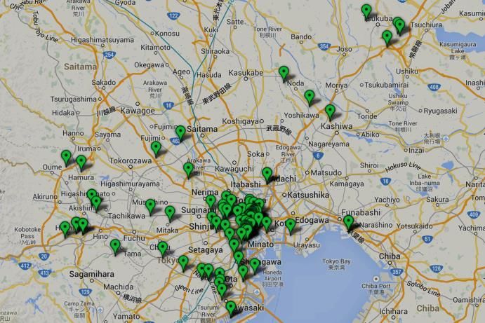
7.1 Nanotech industry landscape map
Nanotech companies in Japan are mostly concentrated among large cities across the
country. Mainly the companies’ headquarters are in and around Tokyo.
Alongside the report, a web application for searching among nanotech companies has
been made.
Figure 6: Map of nanotech companies in Japan
On the website of the EU-Japan Centre for Industrial Cooperation (http://www.eu-
japan.eu/interactive-map-nanotech-cluster-and-industry-landscape-japan), one can
find an interactive map that shows companies involved in nanotechnology.
Figure 7: View of nanotech companies in Tokyo area
The map is interactive and further details (contacts, activities, locations, etc.) are
displayed while sliding over the green marker.
24Japanese Nanotech Cluster and Industry Landscape
Figure 8: Nanotech interactive map with company details.
Source: http://www.eu-japan.eu/interactive-map-nanotech-cluster-and-industry-landscape-japan
7.2 Nanotechnology industry landscape
Japanese nanotechnology industry landscape is very diverse. In Japan there are over 600
companies37 related to nanotechnology and this number is increasing daily. The report
covers 150 major Japanese companies38, active in the nanotechnology field.
These companies were separated into five categories:
- Equipment (companies that have activities in the field of equipment, machinery and
device manufacturing)
- Research and development (companies that have activities in R&D of
nanotechnology)
- Materials (companies that have activities in the field of materials)
- Products (companies that have activities or are selling nanotechnology related
products)
- Service (companies offering services related to nanotechnology)
Many companies are operating in more than one field, therefore, included in multiple
categories. Out of 150 profiled companies, there are 57 companies operating in the
“equipment” field, 51 in “materials”, 38 in “products” and 47 active in “research and
development” field and 25 in the field of “services”.
Traditionally, strong equipment manufacturing is also emphasized in the nanotechnology
landscape. There is a variety of companies involved with development in “hardware” for
nanotechnology; there are many already established and new companies in various niche
segments.
37 Source: JETRO
38 Data obtained through internet, interviews, literature. Database is found in the annex
25Japanese Nanotech Cluster and Industry Landscape
Likewise activities in materials are also abundant in the Japanese nanotech sector.
Companies are developing new, innovative and improved materials. Many of them are
pioneers and leading in the world segments.
In the annex are compiled databases of 150 Japanese companies that have activities in the
nanotechnology sector.
7.3 Nanotechnology industry landscape graphic display
Below is a graphic display of the Japanese nanotechnology landscape. Compiled into five
groups: Material, Equipment, Product, R&D and Services.
Figure 9: Nanotechnology business landscape in Japan
26Japanese Nanotech Cluster and Industry Landscape
8. Nanotechnology in European Union and supporting
programs
Nanotechnology in European Union has been set as a priority research topic. In the largest
open research fund Horizon 2020 nanotechnology is considered a key enabling technology
(KET). From 2014 until 2020 near to 4 billion euros will be invested into nanotechnology
research projects in the EU.
Japanese individuals and organizations have the opportunity to participate in these projects,
gaining access to EU research area and potential market advantage. Following are described
the key institutions that can assist with applying to Horizon 2020 funds, searching for
partners and acquiring information on this matter.
8.1 Horizon 2020
Horizon 2020 is a Framework Programme for Research and Innovation created by the
European Union in order to implement the Innovation Union flagship initiative by
encouraging and supporting collaborative R&D and innovation for the competitiveness of
the EU39. The programme will run from 2014 to 2020 and provides an estimated €80 billion
of funding for research and innovation projects as well as other supporting activities. This is,
if not unique, one of the largest research funds open to the entire world.
"Leadership in enabling and industrial technologies" is under “Industrial Leadership”, one of
the 3 priorities of the programme with the budget of 14 billion euros and focuses on areas
with strong industrial dimension and potential to drive innovation, such as Information and
communication technologies (ICT), Key Enabling Technologies (KETs), and space.
8.2 Key enabling technology – Nanotechnology
Nanotechnology is considered as a KET and therefore is a priority topic for R&D in the
Horizon 2020. Dedicated funds for nanotechnology are 3.85 billion euros until year 202040.
Although Japan is not eligible for automatic funding from the EU, Japanese organizations and
individuals can join the projects, potentially with the following benefits:41
- Creation of a large network with top class research organizations and researchers in
the EU
- Role in standardization and rulemaking, therefore a key market advantage
- Access to databases not available in Japan and/or devices not (yet) authorized in
Japan
- Possibility of doing technology watch
The participation enables researchers; research organizations and companies to have direct
access to newly developed technologies and therefore permits them to be the first in
capitalizing innovations. Japanese subsidiary companies in Europe are eligible for Horizon
2020 funds as European legal entities.
39 Horizon 2020 framework programme. http://ec.europa.eu/programmes/horizon2020/
40 Horizon 2020, Key enabling technologies. http://ec.europa.eu/research/industrial_technologies/policy_en.html
41 JEUPISTE presentation 2014
27Japanese Nanotech Cluster and Industry Landscape
8.3 JEUPISTE
Japan-EU Partnership in Innovation, Science and Technology (JEUPISTE) is a project co-
financed by FP7 (Framework Programme prior to Horizon 2020) aiming to promote EU-Japan
bilateral cooperation in Science, Technology and Innovation (STI) through support to STI
policy dialogues, deployment of bilateral information services, organization of
academic/innovation workshops, networking events, etc.
JEUPISTE is a consortium of 10 partners from Japan and Europe, coordinated by the Institute
for International Studies and Training of which the EU-Japan Centre for Industrial
Cooperation is a branch42.
8.4 Horizon 2020 - National Contact Point Japan
The EU-Japan Centre for Industrial Cooperation has been nominated as the National contact
point (NCP)43 in Japan for Horizon 2020.
Supported by the Japanese government, NCP in Japan offers accessible and free of charge,
impartial and confidential services for all types of organizations interested in participating in
Horizon 2020 and tailored to the needs of each individual businesses and organization. The
services include:
- Guidance on choosing relevant Horizon 2020 topics and types of action
- Advice on administrative procedures and contractual issues
- Assistance on proposal preparation
- Distribution of documentation (forms, guidelines, manuals etc.)
- Assistance with consortium building (in cooperation with the Enterprise Europe
Network, if appropriate)
- Information on other European opportunities
8.5 Enterprise Europe Network (EEN)
Enterprise Europe Network is an international network of close to 600 partners, committed
to providing excellent customer service to clients across 48 countries. The partnering
organizations which are members of the Enterprise Europe Network offer support to small
and medium-sized companies in the fields of international business cooperation, innovation,
knowledge and technology transfer, financial sources and participation in EU-funded
programmes.
Main support activities:
- Support to the B2B Partnering Process
- Online database with 20,000 partnership requests and offers (http://www.een-
japan.eu/content/network-database)
- Selective search for partnerships in business or technology transfer
- Support to matchmaking events in Europe
- EEN co-organizes brokerage and matchmaking events across Europe to facilitate face
to face B2B meetings
- Information Service – inquiry helpdesk
- Provision of sources of information on EU Market, regulations and innovation
EU-Japan Centre for Industrial Cooperation is the coordinator for EEN in Japan44.
42 More information at http://www.jeupiste.eu
43 More about NCP at http://www.jeupiste.eu
44 More about EEN on: http://www.een-japan.eu
28Japanese Nanotech Cluster and Industry Landscape
9. Business opportunities
In developing a broad market for nanotechnology, business opportunities are abundant.
Nanotechnology being a sector based on disruptive innovation, there are many fields of
potential application. Japan is more open to new advanced technologies that can be
implemented into their product spectrum, but on the other hand quite closed for entire
products from overseas. For companies in the sector to be successful, they must meet high
Japanese standards and receive the best references which is sometimes very challenging
Japanese strengths in the nanotechnology field45:
Materials – The Japanese research and development field is constantly pursuing new
materials for further improvements. The following companies have discovered new
materials: NEC, Hitachi, Flox Corporation, Hodogaya, Toshiba, etc. Most emphasized
are carbon nanotechnology products – CNTs, Fullerenes, Multi-walled carbon
nanotubes.
Equipment - Traditionally, Japanese companies are strong in high-tech research and
manufacturing equipment and devices. Companies such as Hitachi, Jeol, Horiba,
Fujitsu and many others, provide equipment for nanotechnology related activities.
Opportunities for EU companies:
Niche markets are open for companies with advanced technologies46 - Testimonials
show that Japan is a good market for niche nanotechnology products, advanced
technologies and materials. Most of the interviewed companies stated that they
didn't have many obstacles with entering the Japanese market and that state-of-the-
art technologies have advantages in the niche markets where some enjoy the lack of
domestic competition. The majority of the Japanese market will always remain
protected and will be harder to access.
Joint R&D projects through Horizon 2020 – In 2014, the EU introduced the world’s
largest open research fund. European companies can create consortiums with
Japanese companies and institutions conducting joint research and development.
This can result in partnerships with both sides that give market advantage through
representation. Final products or technologies that are the end-result of the projects
can be more easily introduced to the Japanese market due to references, links and
information gained through Horizon 2020 projects.
Japanese companies want “future” technologies 47 - Experience shows that
Japanese companies are interested in new foreign technologies. While large
Japanese companies still have well established markets in Asia and the US, and have
an immense reach in the region, due to the increasing developments in China and
Korea, Japan is sometimes struggling with keeping its presence in the markets. The
Japanese by nature emphasize the optimization than innovation. Therefore, foreign
advanced technologies are welcomed. Although implementation and technology
transfer can take much time, the results can be well compensated.
45 Information acquired through interviews
46 Information acquired through interviews
47 Information acquired by author through business development experience
29You can also read