Self-aligned process for large scale fabrication of CNTFETs
←
→
Page content transcription
If your browser does not render page correctly, please read the page content below
Chapter 4
Self-aligned process for large
scale fabrication of CNTFETs

                                 69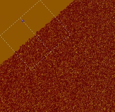
In the previous chapter, C-AFM measurements have shown that the catalytic areas (Al/Ni) are
conductive. It sounds logical since Al and Ni are metals. Based on this fact, the first attempt
to fabricate CNTFETs is to use the catalyst directly as SWNT contacts, by patterning catalytic
pads separated by a narrow gap (5 to 50 µm). When SWNTs, which start to grow from one
pad, reach the second one, the pads can be directly used as source and drain electrodes. In
section 4.1, the mask used for source/drain patterning is described, as well as the setup for
CNTFET measurements. In section 4.2, some preliminary results of successful fabrication and
measurement of CNTFETs with Al/Ni catalytic areas as S/D electrodes are presented. However,
the devices exhibit poor electrical performances. To prove that CNTFETs are potential candidates
for replacing conventional MOSFETs, and that the in situ growth of SWNTs is a suitable method
for CNTFET fabrication, novel integration concepts are developed and tested. These concepts
are reported in sections 4.3 to 4.4.

4.1 Preparatory work

 4.1.1 Mask for optical lithography

  The mask used for patterning source and drain electrodes has been designed and fabricated
at ISTN. The layout of the mask is represented in Fig. 4.1a. The wafer is divided into four parts:
  1. The top right corner contains five chips with 102 regular CNTFETs and one chip with 34
     CNTFETs. The layout of a single device is drawn in Fig. 4.1b. It is very simple. Source
     and drain are separated by a rectangular region, the length of which is called S/D spacing
     and is equal to the nominal channel length (Lnom ) of the transistor. The nominal device
     width (Wnom ) is defined as the width of the S/D metal bars, as indicated in Fig. 4.1b. S/D
     electrodes extensions are large quadratic pads of 0.01 mm2 . Each chip contains CNTFETs
     with different channel geometries. Lnom is ranging from 1.6 µm to 4 µm in 0.2 µm intervals
     and from 4.5 µm to 6 µm in 0.2 µm intervals. Wnom is ranging from 5 µm to 25 µm in
     0.5 µm steps and one fixed value of 50 µm.
  2. In the bottom right corner, special devices with very wide S/D electrodes (see Fig. 4.1c)
     have been designed. Lnom is ranging between 1.8 and 2.2 µm. Wnom is equal to 100 µm,
     500 µm or 1000 µm. These structures are used to obtain a device with high current when
     SWNT growth occurs selectively, i.e., only s-SWNTs and no m-SWNTs are obtained.
  3. In the bottom left corner, two chips have been drawn especially for C-AFM measurements
     which require an electrical contact to the AFM chuck (see subsection 4.3.1). The chips are
     identical with the ones of the top right region except that the left electrodes of the 102
     devices of the chip have a common drain, linked to a mm scale pad which can be soldered
     to a usual wire (see Fig. 4.1d). The other extension of the wire can be clipped to the AFM
     chuck.
  4. Finally, CNTFETs included in special frames are drawn in the top left corner. The frames
     contain alignment marks for an eventual utilization of the electron beam lithography as
     a second lithography step (which has not been tried yet). Otherwise, the transistors are
     designed like the regular devices situated in the top right corner (see Fig. 4.1b) and can be
     measured in the same way.

Chapter 4. Self-aligned process for large scale fabrication of CNTFETs                         71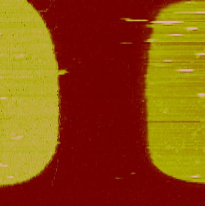
There is a total of 923 transistors on one wafer. In the next sections of this chapter, the devel-
opment of a novel process for CNTFET fabrication is reported, in which all devices of the mask
are processed simultaneously. This is the reason why the process can be referred as “large-scale
integration” of CNTFETs and this fact alone constitutes one of the major novelties of this PhD
work. Statistics on yield are reported in section 5.1 in the next chapter.

                                                                    wafer

                                               6 regular CNTFETs chips
                        2 CNTFETs chips         1 chip = 102 CNTFETs
                         for alignment          with 17 different L nom
                         with electron           and 6 different Wnom
                       beam lithography

                                                                                                 Drain

                                                                          Special transistors
                                                                              with very                             S/D
                                                                           wide electrodes        S/D             spacing
                    2 CNTFETs chips
                       for C-AFM                                             (>100 μm)           width
                     measurements
                                                                                                         100 μm
                                                                                                                  Source

                                                                                                                  100 μm
                                                                                                (c) special transistors

                                                 mm scale pad to be          102 CNTFETs with
     (a) whole mask                              manually connected       common drain electrode
                                                   to AFM chuck

         Drain             S/D        Source                                           100 μm
                         spacing
      S/D width = Wnom
                            =
                          L nom                         5 mm

        100 μm           100 μm       100 μm
     (b) regular transistors                   (d) chip for C-AFM measurements

Figure 4.1: (a): Layout of the whole mask used for lithography step. (b) to (d): Details of the mask layout
            representing CNTFETs with different geometries.

72                                                                                                  4.1 Preparatory work
4.1.2 Semiconductor parameter analyzers

  After fabrication is completed, the processed CNTFETs should be electrically evaluated with
a semiconductor parameter analyzer. Initial electrical tests have been performed with the
HP 4145B, which is a somewhat older measurement setup. Off-state leakage measurements
(Io f f ) are limited by the equipment to 10−10 A because of oscillations between -100 and 100 pA.
With this setup, the quality of the fabricated devices regarding the on/off ratio parameter can-
not be correctly evaluated (see Fig. 4.15). Neither Io f f nor the on/off current ratio (Io f f /Ion )
were calculated because they would have been misleading. Later on, a new measurement setup
was installed at the ISTN, the Keithley 4200. This very modern setup for semiconductor device
analysis allows the measurement of off-state leakage currents down to some tens of femto-
Amps (10−15 A) when using preamplifiers which are placed immediately near the wafer within
the measurement box of the wafer prober. Most sweeps presented in this dissertation have been
measured with the Keithley setup. Nevertheless, some important preliminary results measured
with the HP 4145B are also presented in the next sections because the non-optimized devices
exhibited a reduced life time and could not be remeasured with the new setup.

4.2 First attempt on CNTFET fabrication using catalytic areas as source/drain electrodes

  The in situ growth of SWNTs developed to build SWNT devices is catalyzed by an Al/Ni double
layer. Since both materials are well-known metals and C-AFM measurements confirmed that the
catalytic areas are conductive (see Fig. 3.22), the simplest way to obtain a CNTFET is to use the
layout of regular transistors (see Fig. 4.1b) to pattern Al/Ni areas, which serves as the catalyst
for SWNT growth as well as metallic S/D electrodes after growth. The Si substrate acts as
the back gate electrode. When a s-SWNT links the source and drain structures of a regular
transistor, a very simple CNTFET is realized. Such a device and its electrical connections are

                    SWNTs grown from Ni clusters                Ids
                                            Vds
                  catalyst                              SWNT acting as channel
                                          drain                                  source
                  (Al/Ni)

                             SiO2

                             Si               gate

                                                  Vgs

      Figure 4.2: Schematic of CNTFET in which catalytic areas are directly used as S/D electrodes.

shown schematically in Fig. 4.2. The AFM in tapping-mode is used to confirm that SWNTs can
really grow from one electrode, extend on the SiO2 (catalyst underlayer) and then reach the

Chapter 4. Self-aligned process for large scale fabrication of CNTFETs                                73
neighborly electrode. Some structures at different places on the wafer have been measured and
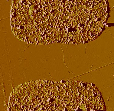
an example of such an AFM measurement is given in Fig. 4.3a. It can be seen that some SWNTs
10-5
10-6
-6 on/off ratio:
10-7 Ion = 1.5 x 10 A
2.0 x 10³
10-8
10-9
Ids (A)
10-10 Ioff = 7.3 x 10⁻¹⁰ A
10-11
10-12
10-13
10-14
-100-80 -60 -40 -20 0 20 40 60 80 100
Vgs (V)
(a) (b)
Figure 4.3: (a): AFM measurement (amplitude) of a CNTFET by which catalytic areas act as S/D electrodes
(b): Example of transfer characteristics measured on such a CNTFET.
grew in the wrong positions, i.e., they do not link the two electrodes. However, one SWNT
grew almost perfectly, because it is nearly perpendicular to both electrodes. SWNTs which link
source and drain diagonaly would also be usable but this geometry would increase the effective
channel length (see subsection 5.3.1). The fabricated CNTFETs are tested using a semiconductor
parameter analyzer and the electrical connections drawn in Fig. 4.2. To be able to have a
detectable current, very high S/D biases such as 30-40 V must be applied. This indicates that the
contacts between SWNTs and electrodes are highly resistive. Also, in order to control the current
flow by the field effect, high gate voltages must be applied because of the thick gate oxide (i.e.,
500 nm). Elevated gate biases in the range of 100 V are used. However, they correspond to
an electric field strength across the gate dielectric of 2 MV/cm, which is a common value in
CMOS applications. In other words, when scaling down the oxide thickness from 500 to 5 nm
for example, the gate voltage will be scaled down accordingly to 1 V. Initially, a very low on/off
ratio of about 4 has been measured on the fabricated CNTFET structures. The transistors are
working like p-type MOSFETs, which means that they are turned off at large positive values of
V g and turned on at negative values of V g . However, the low on/off ratio of 4 indicates that both
s-SWNTs and m-SWNTs link the contacts, as expected from the standard CVD growth which is
not selective with respect to the chirality. According to theoretical considerations, approximately
30% of SWNTs are metallic. Metallic SWNTs short circuit S/D electrodes. In order to improve
the switching characteristics of the CNTFETs, the parasitic m-SWNTs must be eliminated. For
this purpose, a process found in literature was used, namely the selective burning of m-SWNTs
[91]: A very short electrical pulse is applied between source and drain, while a positive voltage
is applied to the back gate during pulsing to turn off and protect the s-SWNTs. In contrast, the
m-SWNTs are still conductive so that the power of the electrical pulse is dissipated and burns
the m-SWNTs away selectively. The on/off ratio of the CNTFETs improves significantly upon
applying this method, at least to a value of 100 for most of the transistors. Fig. 4.3b shows one
74 4.2 First attempt on CNTFET fabrication using catalytic areas as source/drain electrodes
example of a CNTFET transfer characteristics (Ids versus V g ) after burn pulse. The corresponding
on/off ratio is equal to 2100. When trying to increase this ratio by applying even higher voltage
pulses (typically more than 300 V), no improvement could be achieved since it mostly lead to a
dielectric breakdown of the gate oxide.
   One solution to this problem is to contact SWNTs with an appropriate metal so that low
contact resistances are obtained, which means that more current will flow through the tubes
(ohmic contacts). Pd is known to provide very good contacts to SWNTs used in p-type FETs
[30] (see also subsection 2.3.2). To fabricate CNTFET structures with a similar process to the
one reported above and to improve them by contacting SWNTs with Pd, a second lithography
step must be processed to align metal electrodes exactly on the catalytic areas. In this case,
the SWNTs lying on the SiO2 still serve as the channel and the SiO2 layer forms the gate oxide.
The end parts of the SWNTs are encapsulated between catalyst and Pd. Fig. 4.4a shows an
illustration of such a structure. However, precise alignment of the metal electrodes on the
catalytic areas is difficult. Even when special alignment marks were used, misalignments could
not be avoided. Fig. 4.4b shows an example of CNTFET structures which are not usable at all as
the alignment of the Pd electrodes on the catalytic areas failed. For all wafers which have been
structured with a double lithography step during this PhD work, it was impossible to obtain well
aligned structures.
                                            Ids
                         Vds
 catalyst Pd                       SWNT acting as channel
                       drain                                source
 (Al/Ni)

         SiO2

         Si                 gate

                            Vgs

                                      (a)                                           (b)

Figure 4.4: (a): Schematic of CNTFET where Pd S/D electrodes are aligned on catalytic areas. (b): Exam-
            ple of AFM scan (height) of a CNTFET fabricated by aligning Pd electrodes on catalytic areas
            showing the difficulty of this process and the misalignment problem.

  Another phenomenon has been discovered by observing the fabricated structures before Pd
evaporation under the optical microscope, as shown in Fig. 4.5a. In some areas, the SiO2 ap-
pears partly covered by an unknown material. AFM measurements (tapping-mode) have been
performed at the limit between covered and non covered SiO2 . The material is found to be a
∼2.6 nm ultra thin layer (see Fig. 4.5b and Fig. 4.5c). Moreover, C-AFM measurements show
that the layer is made of a conductive material (see Fig. 4.5d and Fig. 4.5e). The layer is prob-
ably composed of carbon, either amorphous or crystalline, resulting from parasitic methane
pyrolysis. Indeed, it has already been reported that pyrolysis of methane can occur during CVD,
especially when no H2 is mixed to CH4 [74]. Pyrolysis is a reaction which chemically decom-

Chapter 4. Self-aligned process for large scale fabrication of CNTFETs                               75
poses organic materials (on the basis of carbon-hydrogen bonds) when they are heated in an
atmosphere free from oxygen or any other possible reagent. N2 , used during annealing directly
before CVD is probably still present in the chamber during CVD but it is an inert gas and does
not participate in chemical reactions. The ultra reduced thickness of the carbon layer could
correspond to a crystalline material, i.e., graphite with only three to four graphene flakes. The
carbon layer often appears near the catalytic areas and probably covers the catalytic areas them-
selves. More problematic, the conductive carbon layer sometimes completely covers the spacing
between source and drain, which shorts the electrodes. CNTFETs with shorted S/D electrodes
are defect. The carbon layer must be eliminated to increase the probability that a CNTFET is
functional.

                          SiO2

                            limit

       SiO2 covered
       with carbon

       Al/Ni after CVD
          without H2

     (a) Optical microscope photograph         (b) AFM scan (height)            (c) height cross section (average)
                                                                                    along all scan lines in the white
                                                                                    box.

                                                             40

                                                             20
                                                           nm

                                                                0

                                                            -20

                                                            -40
                                                                0.0     0.5     1.0    1.5     2.0
                                                                                µm
                         (d) C-AFM current scan                 (e) cross section in the white box

Figure 4.5: Investigation of the parasitic carbon layer by optical microscope, AFM and C-AFM. The ultra
            reduced thickness of the layer could correspond to a graphite layer with only a few graphene
            flakes.

76                         4.2 First attempt on CNTFET fabrication using catalytic areas as source/drain electrodes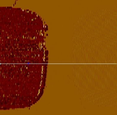
4.3 Development of a novel fabrication process based on “sacrificial catalyst” for high
    on/off ratio CNTFETs

 4.3.1 Introduction to “sacrificial catalyst” and C-AFM measurements

   In the previous section (4.2), it has been established that a carbon layer partly covers the
wafers after SWNT growth and sometimes shorts S/D electrodes. Since the parasitic carbon
layer probably results from CH4 pyrolysis when no H2 is mixed to CH4 during CVD [74], it was
decided to add H2 to CH4 during SWNT growth. H2 inhibits the pyrolysis of methane as it is
itself a product of the pyrolysis reaction (see equation (4.1)). The system moves toward its new
equilibrium which should be the reverse reaction (production of methane). The production of
methane is of course, under the given time and pressure conditions, impossible.

                                                C H4 → C + 2 H2                                    (4.1)

 As a result, no carbon layer is visible on the wafers, neither under the optical microscope nor
under AFM/C-AFM. Moreover, the Al/Ni catalytic layer itself is not conductive anymore after
SWNT growth. Initial simple measurements on the catalyst area indicate that the metal converts
into an insulating material. We call it “sacrificial catalyst”. We suspect that the conduction of
the catalyst reported previously was due to the ultra thin carbon layer covering the catalyst,
which would also explain why such high drain/source voltages (30 V) had to be applied: The
resistance of a 3 nm thin carbon layer is excessively elevated.
  Detailed investigation of the sacrificial catalyst are performed with C-AFM. For this task, spe-
cial wafers have been produced, in which large areas of Al/Ni catalyst have first been structured
on the SiO2 . Subsequently, Pd contacts have been patterned on them using the mask described
previously in section 4.1. As a result, two topographical steps are formed: Pd to catalyst and
catalyst to SiO2 (see Fig. 4.6). The large pads of the special chips for C-AFM measurement (see
Fig. 4.1d) are connected manually to the AFM chuck. An example of such a C-AFM measure-
                                                Itip
                                  AFM tip                 AFM

                                                           SWNT
                    sacrificial      Pd                                   Pd
                     catalyst

                          SiO2

                           Si

                                                                   AFM chuck
                                              Vchuck

              Figure 4.6: Schematic of test structure for AFM sacrificial catalyst investigation

Chapter 4. Self-aligned process for large scale fabrication of CNTFETs                                77
ment using a structure located within the C-AFM test chips of the wafer is shown in Fig. 4.7. In
the topographical scan (Fig. 4.7a), the steps formed by the Pd pads on the catalyst structure and
by the catalyst on the SiO2 are visible. The cross section (see Fig. 4.7c) shows two topographical
steps: the catalyst on the oxide and the palladium on the catalyst. In contrast, the step formed
by the Al/Ni on the SiO2 is invisible in the current image (Fig. 4.7b), which is also evident in
the current cross section (Fig. 4.7d). Only the conductive Pd area can be identified. The catalyst

                           (a) C-AFM (height) scan                            (b) C-AFM (current) scan

               80                                                 40
               60          Pd
               40                                                 20
               20
                                                                              Pd
              nm

                                                                 pA

                   0                  catalyst       SiO2             0
                                                                                         non-conductive area
               -20                                                                         (SiO2 + catalyst)
               -40                                               -20
               -60
               -80                                               -40
                       0    2    4        6      8          10            0    2     4        6     8      10
                                     µm                                                  µm
                           (c) height cross section                           (d) current cross section

Figure 4.7: Comparison of C-AFM height and current scans on structured sacrificial catalyst. (a) and (c)
            show that the geometrical step created by the sacrificial catalyst is still visible whereas in
            (b) and (d), only the Pd electrode is visible. Both sacrificial Al/Ni catalyst area and SiO2 are
            nonconductive.

layer has the same color as SiO2 , corresponding to 0 pA. However, the thin layer of Ni on Al was
initially conductive, as proved by simple surface measurements before CVD. The Al most likely
converts into Al x O y (i.e., a high-κ dielectric) due to:

     1. reaction with SiO2 during the high-temperature step (i.e., oxidation of the lower part of
        the Al layer at the SiO2 interface).

     2. reaction with the ambient oxygen/water. The 1 nm Ni film turns into separated nickel
        nanoclusters during CVD. This discontinuous Ni layer allows ambient air contact from

78      4.3 Development of a novel fabrication process based on “sacrificial catalyst” for high on/off ratio CNTFETs
the top, resulting in the oxidation of any residual metallic fraction in the top part of the
aluminum layer.
To the best of our knowledge, C-AFM measurements of the metallic to dielectric conversion of
the catalyst used for in situ SWNT growth has been observed and published for the first time
within this PhD (see list of publications and conference contributions, 2).
4.3.2 CNTFET fabrication process and associated C-AFM characterization method
The previous experiment confirms that the catalyst can be used as a “sacrificial” layer: since
it converts into a dielectric, it is not necessary to pattern it. It is sufficient to structure metal
pads on the wafer after SWNT growth. When the nanotubes grow with an appropriate density,
on average one single SWNT ideally links source and drain, i.e., its end parts are encapsulated
between catalyst and source/drain whereas its center part lies on top of the catalyst. Even if
the converted catalyst covers the entire wafer surface, it does not short circuit devices laterally
and allows the vertical electric field of the gate to penetrate and control the current flow within
the active part of the SWNTs. Such a process is self-aligned, i.e., only one step lithography is
required. Thus, the problem of the misalignment of the palladium pads on catalyst as shown in
section 4.2 is solved. To the best of our knowledge, such a fabrication process on the basis of
metallic catalyst which turns into a non conductive material after in situ SWNT growth has been
developed and published for the first time as a result of this PhD work (see list of publications
and conference contributions, 5).
Description of fabrication steps
Fig. 4.8 summarizes the 12 steps of this novel CNTFET self-aligned fabrication process.
Since the substrate is used directly as a back gate electrode, it should have a high conductivity
equivalent to a metal. It has been decided to use 2 inches, highly p-doped (boron) wafers, the
resistivity of which is situated between 0.01 and 0.02 Ohms. Prior to the covering and patterning
of the different layers, the wafers are labeled on the back side with a diamond pen and then
cleaned in three steps: a standard cleaning, a special cleaning used when the growth of a very
thin gate oxide is the subsequent step and a hydrofluoric acid (HF) short cleaning (“HF-dip”).
The standard cleaning consists of two sulfuric acid (H2 SO4 ) baths, one at 100°C, the other at
room temperature. The special cleaning is called piranha cleaning and is composed of sulfuric
acid mixed with hydrogen peroxide (H2 O2 ) in ratio 4:1. The wafers are immersed during 15 min
in each of the three baths so that a thin layer of SiO2 grows on the silicon surface which also
aids in the elimination of the organic residue. The native oxide layer is finally removed in a
hydrofluoric acid (HF) bath diluted in de-ionized water (1:22) during 30 s (HF-dip). After the
HF-dip, the wafers must be oxidized within a short time otherwise the native SiO2 will grow
again from ambient air. The thermally SiO2 is grown on the whole wafer and must have a very
good quality as it serves as the gate oxide. It isolates the SWNTs used as the channel from the
Si-substrate used as the back gate electrode (see Fig. 4.9a). As the SiO2 thicknesses necessary
for the experiments are only between 30 and 100 nm, the dry oxidation process takes place at
1000°C with a growth time of 30 min and 5 h respectively. Dry oxidation is preferred because it
produces a better oxide quality than wet oxidation.
Chapter 4. Self-aligned process for large scale fabrication of CNTFETs 79Labeling E-beam
Dry - evaporation
+ -
Cleaning oxidation of Al/Ni
Oxygen CCVD
- - Annealing -
plasma of SWNTs
Resists Resists
- spin coating - Exposure -
development
+ Postbake
E-beam Back side
- evaporation - Lift-off - etching
of Pd in HF
Figure 4.8: Steps of the self-aligned fabrication process for Pd-connected CNTFETS.
For the next step, ultra thin layers of Al (5 to 7 nm) and Ni (0.5 to 1 nm) are evaporated
on the entire wafer surface by means of electron beam evaporation (see section 3.1). Note
that no patterning of this catalyst is required. Subsequently, the wafers are annealed to about
870°C in the CVD reactor in N2 at atmospheric pressure for 5 min to form Ni nanoclusters,
which act as catalyst particles for SWNT growth (see Fig. 4.9b). The next step is the SWNT
growth, which takes place for 10 min in a CH4 /H2 mixture without changing the temperature
or taking the wafers out of the reactor. H2 is used during growth to prevent carbon deposition
on the wafers during CVD, as described in the previous section. SWNTs are grown on the entire
surface of the wafer (see Fig. 4.9c). As already mentioned, the Al/Ni catalyst converts into an
Al x O y film (i.e., high-κ dielectric), which is covered with discontinuous Ni nanoclusters after
the high-temperature step.
Lastly, Pd S/D electrodes are structured and placed all over the wafer without need of align-
ment using the lift-off method. This step requires primarily that the wafers are heated for 2 h
in a dry chamber to remove humidity. Then, an adhesion promoter (A1100) is applied under
vacuum. For the photolithography, a two-layer-system from All Resist is used [92], instead of
a conventional one-layer photoresist to simplify the lift-off step. PMMA (polymethyl methacry-
late), a copolymer based on methyl methacrylate and methacrylic acid, is spin-coated and dried.
A positive photoresist (novolac-naphthoquinondiazide combination) is brought on top of this
tempered copolymer layer (see Fig. 4.9d). Only the photoresist is photosensitive and the ex-
posed parts are removed in the developer (positive resist). The PMMA layer does not react with
light but is removed by the developer at a defined rate. The removal is isotropic and undercuts
are formed (see Fig. 4.10). After lithography, the wafers are covered with Pd by electron beam
evaporation. During the collimated evaporation, the wafers lie above the Pd source. The wafer
80 4.3 Development of a novel fabrication process based on “sacrificial catalyst” for high on/off ratio CNTFETsAl Ni
SiO2
Si
SiO2
(a) After evaporation (b) After annealing
st
to resi
pho
MA
PM
SiO2
Si
SiO2
(c) After SWNT growth (d) After spin coating, exposure and development
(e) After lift-off Final structure
(f) (after back-side etching)
Figure 4.9: Schematic of intermediate steps and final structure of the fabrication process for CNTFET re-
ported in this chapter.
Chapter 4. Self-aligned process for large scale fabrication of CNTFETs 81Figure 4.10: SEM micrograph of the undercut formed by the PMMA under the photoresist. holder is not rotating (see Fig. 3.3) so that the undercuts are not covered with Pd. The Pd layer which covers the photoresist mask is clearly separated from the Pd structures on the substrate so that the photoresist is lifted-off easily in a solvent based on NMP (N-Methyl-2-pyrrolidone). When using only standard photoresist, the lift-off step is very difficult since a continuous metal layer covers the whole wafer: the photoresist sides are not perfectly vertical (see Fig. 4.10), which consequently means that the sides are covered with Pd as well. The final step is the SiO2 etching of the back side of the wafer with a drop of HF because the silicon substrate, which is used as the back gate electrode, must have electrical contact to the wafer prober chuck (see Fig. 4.9f). The wafer is then rinsed with water and dried. Associated C-AFM process characterization The C-AFM measurement method is extensively used for process control during the production of CNTFETs on sacrificial catalyst. Three different C-AFM applications on transistor structures are described below. First, when performing an AFM scan in tapping-mode on the sacrificial catalyst, it is some- times impossible to identify SWNTs due to the enhanced surface roughness in the presence of nickel clusters on Al x O y . The image contrast is largely degraded so that clusters cannot be distinguished from SWNTs, as evident in Fig. 4.11 top row. However, a method of character- izing SWNTs also on the rough catalytic area is necessary. For that, C-AFM is used. Indeed, the problem of the rough underlayer which is degrading the detectability of SWNTs is absent in the C-AFM image when the underlayer is insulating. Regardless of the surface roughness of the oxidized sacrificial underlayer, the current level of the background signal will remain close to 0 pA when scanning this electrically insulating layer. Using this approach, it is possible to identify SWNT structures grown on rough catalysts by means of C-AFM. Unambiguous current images are obtained, as shown in Fig. 4.11 bottom row as an example of such a measurement. For this measurement, the C-AFM test chips located in the bottom left corner of the wafer (see Fig. 4.1d) are used, after their common drain electrode has been soldered manually to the AFM- chuck. When a scan is performed in close proximity to connected areas, SWNTs electrically 82 4.3 Development of a novel fabrication process based on “sacrificial catalyst” for high on/off ratio CNTFETs
connected to the Pd can be detected in the current images. Fig. 4.11c shows an example of
such a measurement with the corresponding current cross section (Fig. 4.11d). In contrast, no
CNT can be identified in the topographical image and in the height cross section obtained by
tapping-mode AFM (Fig. 4.11a and b). To the best of our knowledge, the C-AFM characteri-
zation of SWNTs on highly rough surfaces has been demonstrated for the first time within this
PhD (see list of publications and conference contributions, 6 and 10).

                                                                5
                                                                4
                                                                3
                                                                2
                                                                1

                                                           nm
                                                                0
                                                                -1
                                                                -2
                                                                -3
                                                                -4
                                                                -5
                                                                  0.0   0.5   1.0   1.5    2.0   2.5   3.0
                                                                                    µm

                (a) Tapping-mode AFM height scan                          (b) height cross section

                                                            100
                                                                80
                                                                60
                                                                40
                                                                20
                                                           pA

                                                                0
                                                            -20
                                                            -40
                                                            -60
                                                            -80                     SWNT
                                                           -100
                                                              0.0       0.5   1.0   1.5    2.0   2.5   3.0
                                                                                    µm

                      (c) C-AFM current scan                              (d) current cross section

Figure 4.11: Comparison of tapping-mode and conductive mode AFM measurements on sacrificial catalyst.
             Although tapping-mode AFM has a very good resolution (see section 3.2), no SWNT are visible
             on the height scan due to underlayer increased roughness (sacrificial catalyst, Al: 10 nm, Ni:
             1 nm). C-AFM current scan in the same wafer reveals SWNTs connected by Pd electrode.

  Secondly, it is possible to evaluate the density of the in situ grown SWNTs by means of C-AFM.
This evaluation is important since it enables an estimation of the average number of SWNTs
which are electrically connected to source and drain electrodes. Different SWNT densities are
required according to the devices which are to be fabricated. For example, a high SWNT density
would lead to devices which have a channel formed by several SWNTs, connected in parallel.
When they are all semiconducting, and some remaining metallic SWNTs are burned with a
current pulse (see section 4.2), high current power transistors can be built. Seidel et al. already

Chapter 4. Self-aligned process for large scale fabrication of CNTFETs                                       83
built such transistors, however, they exhibit reduced on/off ratios, probably due to a damaging
of the s-SWNTs during the burning of the m-SWNTs [93]. If the targeted devices are high
on/off ratio FETs, only one SWNT should form the channel, i.e., the density of the in situ grown
SWNTs must be reduced. Fig. 4.12 shows three examples of different densities of SWNTs,
measured once again on C-AFM test structures. The three scans show clearly that different
SWNT densities can be reached with the growth process presented in this PhD work, which is a
great advantage compared to ex situ growth methods where SWNTs are randomly dispersed on
wafers and a reliable control of SWNT density is not possible.
(a) low SWNT density (b) intermediate SWNT density (c) high SWNT density
Figure 4.12: Utilization of C-AFM scans (current images) to evaluate SWNT density.
Last but not least, the C-AFM measurement method allows the distinction of structures in
which SWNTs are electrically linking source and drain or not. For these experiments also, the
CNTFETs with a common drain, which is manually connected to AFM chuck are used (C-AFM
test structures). Two kinds of C-AFM scans are obtained, as shown in Fig. 4.13, which in fact
differ only in the current image. The left column shows a structure which does not have any
SWNT link between source and drain: the drain is invisible in the current image as well as in the
current cross section. In contrast, the right column shows measurements of a structure in which
source and drain are connected by at least one SWNT, since the drain electrode is visible in the
current image. The SWNT which links the electrode is also visible in the scan. Unfortunately,
the top part of the SWNT is located outside of the scan field. This method provides a new way
to test device operation and locate defective devices, at the nanometer scale, in situ and without
damaging the fabricated device structures.
4.3.3 Macroscopical electrical measurements of CNTFETs
Fig. 4.14 shows the schematic of structure electrical connections of a CNTFET fabricated with
the process based on sacrificial catalyst reported previously. The Pd contacts are used as usual
S/D electrodes and the silicon substrate acts as the back gate electrode.
Systematic optimization of catalyst thickness
84 4.3 Development of a novel fabrication process based on “sacrificial catalyst” for high on/off ratio CNTFETs(a) C-AFM scan (height image) (b) C-AFM scan (height image)
(c) Associated current image (source con- (d) Associated current image (source con-
nected manually to AFM-chuck) nected manually to AFM-chuck)
200 200
150 150
100 100
50 50 current on CNT
pA
pA
0 0
no "real"
-50 current -50
-100 on drain -100
current current current
-150 on source -150 on source on drain
-200 -200
0 1 2 3 4 5 6 0 1 2 3 4 5 6
µm µm
(e) current cross section (f) current cross section
Figure 4.13: Detection of CNT linking S/D with C-AFM. Link column: no CNT link, right column: with CNT
links.
Chapter 4. Self-aligned process for large scale fabrication of CNTFETs 85Ids
Vds
SWNT acting as channel
sacrificial catalyst Pd drain source
SiO2
Si gate
Vgs
Figure 4.14: Schematic of electrical measurement setup for CNTFET characterization.
After having measured several batches of CNTFETs fabricated with different parameters, it
could be confirmed that the choice of the catalyst thickness is decisive, not only to obtain the
selective growth of SWNTs over MWNTs, and the appropriate density of SWNTs on the wafer,
but also to obtain the requested insulating properties of the catalyst after growth. Several
catalyst thicknesses have been tested. Their influences on the CNTFET electrical measurements
are summarized in Table 4.1.
Al (nm) Ni (nm) Quantity of working devices
8 1 Devices do not have any functionality: S/D electrodes are shorted.
3.5 0.8 Only devices with very large S/D width (>100 µm, see Fig. 4.1c).
5 0.9 Big majority of working devices. Optimal thickness.
Table 4.1: Influence of catalyst thickness on the quantity of working CNTFETs.
If the aluminum layer is too thick (e.g. 8 nm), it cannot be completely converted in Al x O y
during CVD so that a remaining conductive layer shorts all devices all over the wafer surface.
Moreover, an excessively increased Al thickness also induces an excessively dense SWNT net-
work on the surface of the wafer, which can be assimilated to a carbon conductive layer. In this
case as well, all devices are shorted.
If the aluminum thickness is drastically reduced (e.g. 3.5 nm), the density of the SWNTs on
the wafer surface is reduced as well: a large fraction of the devices do not have any SWNT as
S/D link at all. On such wafers, only the devices with very wide S/D contacts (see Fig. 4.1c) are
working.
An optimized catalyst thickness should provide exactly one SWNT per device for the small
S/D width (e.g. Wnom =5 µm) combined with a complete conversion of the catalyst layer into
a non-conductive (“sacrificial”) layer. This happens when using 0.9 nm of Ni on 5 nm of Al
86 4.3 Development of a novel fabrication process based on “sacrificial catalyst” for high on/off ratio CNTFETsas catalyst: The devices are rarely leaky and more than half of them have at least one SWNT
linking S/D. This combination is used for all the following tests reported in this section, and
section 4.4 and chapter 5 as well. The only geometrical parameter which differs from wafer to
wafer is the SiO2 thickness: It varies from 30 to 90 nm in most cases and for a few wafers, a
250 nm thick oxide is used.
Characteristics of fully functional CNTFETs
When the catalyst thickness is optimized (0.9 nm of Ni on 5 nm of Al), numerous fully func-
tional CNTFETs can be measured. Fig. 4.15 shows an example of transfer characteristics mea-
sured on a device with semiconducting SWNT as the channel. The current-voltage sweep has
the typical form of a FET transfer characteristics. The drain-source voltage is set to -400 mV for
all transfer characteristics presented in this work. The transistor is unipolar PMOS-like, which
10-5
On-current: 1,5 µA
10-6
10-7
10-8 slope: 232 mV/dec
Ids (A)
10-9
Measurement setup
10-10 leakage limit
10-11 hysteresis:
0.79 V
Vth,f = 0.32 V Vth,b = 1.11 V
10-12
-3 -2 -1 0 1 2 3
Vgs (V)
Figure 4.15: Example of transfer characteristics obtained on a CNTFET fabricated with the self-aligned
fabrication process reported in this section. SiO2 thickness: 50 nm.
means that the device turns off at positive values of V gs and turns on at negative values of
V gs . This implies that mainly holes participate in the conduction and the electron conduction
is being suppressed. This observation corresponds to the theoretical expectations presented in
chapter 2 on Pd contacted CNTFETs: Pd contacted CNTFETs are unipolar, due to the ohmic
contacts to holes, i.e., the Schottky barrier seen by the holes is almost equal to 0 eV at negative
gate voltages, leading to a high on-current whereas the Schottky barrier is high and wide for the
electrons at positive gate voltages, inhibiting both thermionic and tunneling emission of elec-
trons and thus a parasitic conduction at positive V g (see Fig. 2.18 and Fig. 2.19). In the transfer
characteristics in Fig. 4.15 however, two different sweeps are plotted. One corresponds to the
measurement of the transistor with back gate voltages ranging from -3 to 3 V (forward sweep)
and the other from 3 to -3 V (backward sweep). In nearly all measurements, Ion and Io f f have
Chapter 4. Self-aligned process for large scale fabrication of CNTFETs 87the same value for both forward and backward sweeps. Only the current in the “sub-V th” part
(i.e., where the transistor switches from the on to off state or inversely) is different. In all mea-
surements, the “sub-V th” part of the forward sweep is always located to the left of the backward
one, i.e., the transistor always needs smaller gate voltages to switch from the on to off state,
as inversely. In thousands of measurements, the contrary has never been observed, not even
once. The fact that forward and backward sweeps are not identical is called hysteresis effect.
The voltage difference between both sweeps is called hysteresis, as expressed in equation 4.2.
h yst er esis = Vth,b − Vth, f , with Vth, f /b threshold voltages of forward/backward sweeps. (4.2)
Hysteresis in CNTFETs is a well-known phenomenon and has been reported by almost all groups
fabricating devices in which SWNTs are lying unprotected on SiO2 surfaces exposed to an ambi-
ent environment. The systematic appearance of the hysteresis effect in transfer characteristics
constitutes one of the major differences between CNTFETs and MOSFETs with conventional
SiO2 as the gate oxide.
For all sweeps presented and evaluated in this work, the hysteresis is calculated as the differ-
ence between the threshold voltages of the forward (V th, f ) and backward (V th,b ) sweeps. The
definition of the threshold voltage of MOSFETs (gate voltage at which the inversion layer or con-
ductive channel first appears between source and drain) are not appropriate because CNTFET
operation relies on a different mechanism to conventional MOSFETs. However, the evaluation
of the threshold voltage of the CNTFETs, roughly defined as the transition between on- and
off-states, should occur reliably so that characteristics and devices can be compared. Such a
threshold voltage equivalent can be obtained graphically from the transfer characteristics, as
illustrated in Fig. 4.15. Three lines are drawn in the graph: a horizontal line ( I = I on ) and two
diagonal lines as an approximation of the sub-V th part. The slopes of the two lines represent the
so-called subthreshold slopes of the transistor. The steeper the subthreshold slope, the narrower
the switching range and the better the transistor. For most devices, both forward and backward
subthreshold slopes are identical. In Fig. 4.15, the forward threshold voltage is 0.32 V. V th,b is
equal to 1.11 V, giving an hysteresis of 790 mV. The subthreshold slope is equal to 232 mv/dec.
Finally, the on-current is equal to 1.5 µA at a drain bias of only -0.4 V. It leads to an on-resistance
(Ron ) of 267 kΩ. This value is fairly larger than the theoretical minimal resistance of SWNTs
(6.5 kΩ [29]). The higher value of the SWNT on-resistance is most likely due to increased con-
tact resistance at the SWNT/eletrode contact and could be decreased by contact improvement,
e.g. electrode annealing in forming gas.
Fig. 4.16 shows four further examples of transfer characteristics obtained on devices with s-
SWNTs as the channel. The devices in Fig. 4.16a to Fig. 4.16c have been measured on three
different wafers, the devices in Fig. 4.16c and Fig. 4.16d on the same wafer at different places.
The sweeps look very similar, with subthreshold slopes around 300 mV/dec. Only the on-current
is found to fluctuate slightly (0.5 to 1.5 µA). We propose three explanations for this fluctution:
1. The SWNTs may have different diameters. If the diameter is above 1.6 µm, the trans-
parency of the Schottky barrier for holes is found to be better than by thinner tubes due to
decreased band gap, leading to higher on-currents [30].
2. Some devices may have a SWNT as the channel which contains defects. This would in-
crease its resistance and decrease the on-current.
88 4.3 Development of a novel fabrication process based on “sacrificial catalyst” for high on/off ratio CNTFETs3. In some cases, excessively tall catalytic particles in the proximity of the SWNTs may cause
a shadowing during the metal evaporation so that a non conformal deposition of metal
occurs, i.e., at some places, the SWNTs may not be perfectly cover by the metal and a
tiny distance between metal and SWNTs exists. This geometrical gap forces the carriers to
tunnel from the SWNT to the contact (or inversely). Carrier tunneling induces increased
contact resistance. An annealing step at high temperature (i.e., higher than 660°C, melting
point of Al [84]) could decrease the contact resistance by decreasing or eliminating the
geometrical gap between SWNTs and metallic electrodes, and improving the adhesion of
Pd on the SWNTs.
10-5 10-5
10-6 On-current: 460 nA 10-6 On-current: 410 nA
10-7 10-7
10-8 10-8
Ids (A)
Ids (A)
S = 337 mV/dec
10-9 10-9 S = 393 mV/dec
hyst. = 0.82 V
10-10 10-10
hyst. = 1.25 V
10-11 10-11
0.84 V Vth 1.66 V 0.24 V Vth 1.49 V
10-12 10-12
-4 -3 -2 -1 0 1 2 3 4 -4 -3 -2 -1 0 1 2 3 4
Vgs (V) Vgs (V)
(a) Wafer 1 (b) Wafer 2
10-5 On-current: 1.8 µA 10-5
On-current: 1.5 µA
10-6 10-6
10-7 10-7
Ids (A)
10-8 10-8
Ids (A)
S = 350 mV/dec S = 262 mV/dec
10-9 10-9
10-10 hyst. = 1.87 V 10-10
hyst. = 0.96 V
10-11 10-11
-0.79 V Vth 1.08 V 0.03 V Vth
10-12 10-12 0.99 V
-4 -3 -2 -1 0 1 2 3 4 -3 -2 -1 0 1 2 3
Vgs (V) Vgs (V)
(c) Wafer 3 (d) Wafer 3
Figure 4.16: Four examples of CNTFET transfer characteristics measured on three different wafers, all with
a SiO2 thickness of 50 nm.
Fig. 4.17 shows an example of output characteristics (Ids versus Vds for different V gs ). Note
that the source electrode is, as for all measurements reported in this dissertation, connected to
the ground whereas the drain electrode is connected to a positive or negative voltage which is
measured in reference to ground. The black vertical line indicates the selected date of Vds of
-400 mV which is used for all transfer characteristics measurements. The output characteristics
are not fully symmetrical. In the negative Vds range, the three typical working regions of MOS-
FET can be recognized. For positive V gs , the device is in the cutoff range. For negative V gs and
Vds < Vds,sat , it is in the linear region. A saturation part can be seen for V gs between -1 and -3 V
Chapter 4. Self-aligned process for large scale fabrication of CNTFETs 89fabricated with conventional lithographic methods using a increase the transconductance. A further step was realized
spacer reduction method [11]. by the introduction of a top gate device by Wind et al.
[14]. The electric field at the nanotube was increased by
improving the geometry of the gate electrode and the
5x10⁻⁶
4. Carbon nanotube transistors and circuits
- 400 mV contact resistance was reduced by a suitable choice of
4x10⁻⁶ contact material resulting -3V -4V Vgs
in further (V) = performance
increased
Semiconducting 3x10
single-walled
-6 carbon nanotubes were -2V
values. Additional progress was made by-4 the creation of
first demonstrated in 1998-6 to show a technologically the first CMOS-like device, where a section -3 of a nano-
2x10 -1V
exploitable switching behavior [12]. Tans et al. applied tube was doped with potassium thus reversing -2 its con-
the -6nanotube
an electric field to 1x10 0V to 5V using a back gate and ductivity type [15]. This 0V device corresponds
-1 to a
Ids (A)
managed to modulate the 1V
0 conductivity over more than 5 complementary NOR gate with a gain larger 0 than unity.
orders of magnitude (Fig. 9).
-6 -1V
Since this first demonstra- Other realizations of CNTFET based circuits
1 include
-1x10 n ear
tion of a carbon nanotube field-effect transistor li simple SRAM-cells as well
2V to 5V as ring oscillators
2 [13].
-2V
(CNTFET) tremendous -2x10⁻⁶progress has been made in im- However, the performance of these devices 3 is poor due
proving the electrical characteristics
-3x10 -6 -3V of the CNTFET. One to associated off-chip wiring, non-optimized 5 device de-
disadvantage of Tan’s arrangement was the back-gate sign, and the fact that only single nanotubes can be used
-4x10⁻⁶ of
dielectric which consisted -4Va thick
v silicon v dioxidevds,sat
layer. as devices. Further, comparison with state-of-the-art sili-
Bachthold et al. [13] -6
replaced
-5x10 siliconds,sat
theds,sat dioxide dielec- con devices requires virtually upgraded CNT-devices in
tric by a thin native Al-1.00O
2 3 layer-0.75
on top-0.50
of a -0.25
patterned 0.00which0.25 0.50
an appropriate 0.75
number of 1.00
tubes work in parallel to
V (V)
Al-gate and were able to lower the gate voltage and to ds increase the lateral dimensions to that of existing devices.
Figure 4.17: Example of output characteristics obtained on device with s-SWNT as channel. The dashed
lines are linear approximations of the sweeps.
(starting at different Vds,sat ) whereas for V gs = -4 V, no saturation region can be seen. This be-
havior can be compared with the simulation of Hoenlein et al. [94] which is shown in Fig. 4.18:
for ideal contacts (i.e., contact resistance values at source and drain are 0 kΩ), a saturation re-
gion is visible for all gate voltages whereas for increased contact resistance at source and drain
contacts, the saturation region is absent for increased negative gate voltages. This confirms the
previous argument that the high value for Ron obtained on our device (i.e., 267 kΩ) is due to
increased contact resistances at source and drain contacts. In the conventional MOSFET, the
Figure 4.18:
Fig. 11. Degradation of theResults from [94]. Left:
ideal transconductance (a) andideal
drive output characteristics.
current (b) Right:
due to source and drain degradation
series of output
contact resistances characteris-
(circles denote an assumed value
ticsoutput
of Rs = Rd = 50 kV). The ideal with characteristics
source and (c) drain
also contact resistances
degrade due kΩ.
of 50resistances
to contact series (d).
so-called pinch-off of the conduction (inversion) channel in silicon is reached at Vds,sat . From
this voltage, the channel which normally links source and drain becomes shorter, the carriers
must tunnel through the non inverted silicon to reach the drain electrode. The tunnel current is
constant for all Vds > Vds,sat , this is why the output characteristics are constant in the saturation
region.
90 4.3 Development of a novel fabrication process based on “sacrificial catalyst” for high on/off ratio CNTFETsIn the positive Vds range, a significant current can be measured even for V gs =0 to +1 V. The
cutoff region is only reached for V gs ≥ 2 V. It can easily be explained by the fact that the source
always stays at 0 V whereas at the drain, negative and positive voltages are applied successively.
Thus, for negative Vds , at the drain side, the gate field is reduced compared to the one at the
source side whereas for positive Vds , the local electric field is increased, leading to a difference
in the Schottky barrier height. This also explains why the current in the positive Vds range is
increased compared to the negative Vds range, due to the effective gate voltage difference, e.g.:
V −V
• V gs = 1 V and Vds = 0.9 V implies a local gate field E g at e = gst ds = 0.1
tox
corresponding to
ox
a 0.1 V voltage at the drain side, which means that the device is still in the on-state when
looking at the transfer characteristics.
• V gs = 1 V and Vds = -0.9 V implies a local gate field E g at e = 1.9
tox
corresponding to a 1.9 V
voltage at the drain side, which means that the device is in the off-state.
Devices with metallic/small band-gap SWNTs as the channel
Not all devices work like the previous ones. Some CNTFETs do not show any gate voltage
dependency at all and Ids is constant. The SWNT which acts as the channel in such devices is
probably an armchair nanotube, the only one without a curvature induced band-gap, i.e., with
allowed wave vectors at the K points (see chapter 2). Accordingly, armchair nanotubes are the
only “real” metallic SWNTs (see subsection 2.2.4). An example of such a device is given in
Fig. 4.19a. The channel of the devices fabricated in this work has a minimum length of 1.6 µm
10-5 10-5
10-6 I = 3.05 µA 10-6 Ion: 564 nA
on
10-7 10-7 Ioff: 251 nA
Ids (A)
10-8 10-8
Ids (A)
10-9 10-9 on/off ratio: 2.24
10-10 10-10
10-11 10-11
10-12 10-12
-4 -3 -2 -1 0 1 2 3 4 -3 -2 -1 0 1 2 3
Vgs (V) Vgs (V)
(a) Metallic SWNT (probably armchair) (b) narrow band gap (n − m = 3 × k, k ∈ Z∗ )
Figure 4.19: Example of transfer characteristics obtained on devices with metallic SWNT as channel.
These devices are considered as non-working.
(see subsection 4.3.2), and devices similar to the one in Fig. 4.19a are reproducible and stable.
This means that long purely metallic SWNTs can be grown with CVD at 870°C. This differs from
the result reported by Seidel on in situ growth of SWNTs based on CCVD from methane [95].
He could not measure any purely metallic SWNTs by devices with channel length above 500 nm,
with the explanation that the growth rate is dependent on the chirality of the nanotube. We did
not notice such an effect in this work. However, the deviation may be explained by the lower
growth temperature of 700°C he used.
Chapter 4. Self-aligned process for large scale fabrication of CNTFETs 91Fig. 4.19b shows a similar transfer characteristic to Fig. 4.19a, i.e., in which Ids seems to be
constant. However, a very reduced gate dependency can be noticed. The SWNT linking S/D
is most likely a quasi-metallic nanotube, with a very narrow band gap due to the curvature
of the tube. This narrow band gap only allows a slight gate field control of the on-current.
Quasi-metallic nanotubes are all zigzag and chiral tubes which are found to be metallic based
on the zone folding approximation of the graphene band structure (see subsection 2.2.4), i.e.,
the (n-m) of which is a multiple of three.
A last category of devices appeared during the measurement of our CNTFETs, as shown in
Fig. 4.20. For these devices, a significantly higher gate dependency than for narrow band gap
SWNT devices (see Fig. 4.19b) is obtained. However, it is not possible to turn these devices
completely off as in the devices in Fig. 4.15 and Fig. 4.16. In Fig. 4.20a, the device shows a
10-5 10-5
10-6 Ion = Ion =
S= 10-6
10-7 3.63 µA 835 mV/dec Ioff = 10-7 9.1 µA S= Ioff =
3.45 V/dec
Ids (A)
Ids (A)
10-8 173 nA 10-8 on/off 528 nA
on/off
10-9 ratio = 21 10-9 ratio = 17
10-10 10-10
hyst. = 0.64 V hyst.= 7.90 V
10-11 10-11
-0.03 V Vth 0.61 V -3.32 V Vth 4.58 V
10-12 10-12
-3 -2 -1 0 1 2 3 -10 -8 -6 -4 -2 0 2 4 6 8 10
Vgs (V) Vgs (V)
(a) (b)
Figure 4.20: Two examples of transfer characteristics obtained on devices with several SWNTs as channel.
At least one metallic SWNT causes drastic reduction in on/off ratio, as well as in subthreshold
slope. SiO2 thickness for both devices: 38 nm.
degraded on/off ratio which is reduced to 21, because the off-current is increased from 100 pA
to 173 nA. The second device (Fig. 4.20b) has been measured with a fairly wide gate voltage
cycling range (-10 to 10 V) but it does not increase the on/off ratio which stays at 17. Moreover,
it can be seen that the slope largely degraded and is about three times less steep as the slope of
the devices with a semiconducting SWNT as the channel (835 mV and 262 mV respectively, for a
cycling range of -3 V to 3 V, see Fig. 4.16). Also, the on-current is fairly elevated. We believe that
the channel of such devices is formed by a semiconducting SWNT in parallel with a metallic one.
In Fig. 4.20a, the metallic SWNT contributes to the total current with 173 nA for all gate voltages
(the off-current) whereas in Fig. 4.20b, it contributes with 528 nA, current which is comparable
to the one of the metallic tube in Fig. 4.19b. This statement is corroborated experimentally in
section 5.2 (see Fig. 5.10). Another explanation for the devices with smaller on/off ratio could
be that the nanotube linking S/D is individual but has a large diameter (∼3 nm) implying a
small band gap and thus a small on/off ratio. However, the SWNT growth has been optimized to
obtain a narrow SWNT distribution around 1 nm, making this second explanation less plausible
than the first one (several SWNTs in parallel).
By comparing the devices in Fig. 4.15 and Fig. 4.16 with the ones in Fig. 4.19, it can be
concluded that the first ones have a channel composed exclusively of s-SWNTs. This leads to
the question of the channel width. It is definitely not Wnom (S/D width) given by S/D electrode
92 4.3 Development of a novel fabrication process based on “sacrificial catalyst” for high on/off ratio CNTFETsgeometry but rather determined by the SWNT diameter multiplied by the number of SWNTs. When several SWNTs link S/D in parallel, the channel width is the addition of the individual diameters of each SWNT. In the examples shown in Fig. 4.15 and Fig. 4.16, in which only one SWNT links source and drain, the electrical channel width is approximately 1 nm (average diameter of the SWNTs grown in this work, see chapter 3). When normalizing to the electrically relevant device width, Ion = 1.5 µA translates to 1.5 mA/µA at Vd =-0.4 V. If the channel is formed by several s-SWNTs in parallel, two cases are possible. Either they have approximately the same diameter, which implies that they have the same band gap. In this case, it is probable that they have the same V th and the same subthreshold slope so that they switch from the on- to the off-state simultaneously. Such devices show an increased on-current compared to the ones with only one SWNT. Or their diameter and thus their band gap is different which implies that they do not switch simultaneously (at the same gate voltage), leading to a substantially degraded subthreshold slope. This could be the case for the isolated devices we measured which exhibit degraded subthreshold slopes. In our CNT process, it is very unlikely that more than two or three semiconducting SWNTs in parallel form the channel. The normalized on-current would be then divided by three, which, however, does not change its order of magnitude. 4.3.4 Analysis and experiments on hysteresis As already mentioned, all CNTFETs show hysteresis in their transfer characteristics, i.e., the forward sweep (V gs increasing) is different to the backward sweep (V gs decreasing). The form of the curves is the same with approximately the same slope but they are shifted horizontally on the V gs -axis. This effect is usually absent in regular MOSFET, except in some special cases, e.g. when wet SiO2 is used to intentionally increase trap density [96] or when using some high-κ oxides [97]. Using very clean and advanced processing, MOSFET can be fabricated free of hysteresis. The situation is more complicated for novel devices like CNTFETs. Nevertheless, if CNTFETs are intended to be used in the future as an alternative to conventional MOSFETs, hysteresis in the degraded transfer characteristics will be a problem and should be eliminated: In CMOS logic technologies, devices must have a well-defined threshold voltage, independent of gate voltage cycling range and direction. On the other hand, however, hysteresis may become a usable effect in emerging technologies like SWNT-based sensors (see section 2.4) or memory applications (see section 5.4). In this work, considerable attention has been given to trying to understand the hysteresis phenomenon in CNTFETs. Before performing advanced experiments on hysteresis, a study of the possible origins of hysteresis as found in literature was performed, and is summarized below. •Water molecules: According to Kim et al., hysteresis is due to charge trapping by water molecules which are located around the nanotubes, including water molecules which are ad- sorbed by the SiO2 (i.e. water which sticks at SiO2 surface) near the nanotubes [98]. To prove their assumption, Kim et al. passivated their devices with the copolymer PMMA (polymethyl methacrylate) and noticed a reduction in the hysteresis effect in their devices. PMMA isolates nanotubes from ambient air and thus from ambient humidity. However, the water which is al- ready adsorbed prior to passivation due to previous rinse cycles still remains. This is most likely the reason why other groups, like the one of Shimauchi et al. [99], report that PMMA passiva- tion of CNTFET does not reduce the hysteresis at all. Another group working on hysteresis [100] reports that even the measurement of the devices in vacuum does not eliminate completely the Chapter 4. Self-aligned process for large scale fabrication of CNTFETs 93
hysteresis when the gate voltage cycling range is increased, which means that at least one part
of the hysteresis effect is not caused by adsorbed water or ambient humidity.
   •Fabrication process induced contaminations: Shimauchi et al. believe that the hysteresis
is due to some contaminations which degrade nanotubes. When cleaning the nanotubes with
a piranha solution (sulfuric acid mixed with hydrogen peroxide), which is supposed to oxidize
and etch the organic contamination occurring during the fabrication process (e.g. from the
photoresist), a substantial reduction in hysteresis is noticed compared to non cleaned devices,
but a part of the hysteresis still remains. Also, Bradley et al. observed an increased hysteresis
in devices covered by an electrolytic layer (sodium poly(styrenesulfonate) or Na PSS), which
provides mobile cations (Na+ ) on the surface of the device [101]. Compared to devices which
they processed, paying great attention to avoid ion contamination, the Na PSS covered devices
show a hysteresis with a width five times greater. However, only the forward sweep is shifted. By
further measuring the devices in a humid environment, the backward sweep is in turn shifted.
   •Reversible injection of charges from SWNTs to SiO2 during sweeping: This explanation
for hysteresis is accepted by most scientists working on CNTFETs [100, 102, 61, 103, 104].
The shift in threshold voltage originates from a reconfiguration of the carriers near the CNTS
when applying a gate voltage. The reconfiguration is based on different traps or charges located
within the SiO2 which change their state depending on the applied V g . From MOS technology,
it is known that the SiO2 has fixed charges and traps in its body and also traps at the SiO2 /Si
interface.
   Accordingly, the causes of hysteresis are apparently a combination of environmental humidity
and charge trapping effects within the oxide. The mechanisms of hysteresis are still not fully un-
derstood. But in ambient air stable and reproducible hysteresis-free CNTFETs have never been
demonstrated: Several hundreds of mV wide hysteresis always remain. Some groups which
have measured their devices under vacuum have obtained hysteresis-free CNTFET transfer char-
acteristics, however, other groups could not confirm the differences between measurements in
ambient air and vacuum.
   In order to understand the hysteresis phenomenon in the devices fabricated within this PhD
work, detailed measurements are performed. The results of five experiments are reported be-
low, followed by a proposition to explain the origins of the hysteresis effect.

Experiment 1: reversibility and reproducibility

  First of all, the influence of the starting gate voltage is tested. The same device is measured
once from -3 V to 3 V and back to -3 V, and once from 3 V to -3 V and back to 3 V. The result-
ing sweeps are identical as shown in Fig. 4.21a, which means that the transfer characteristics
are reproducible whatever the previous history of measurement cycles. The mechanism induc-
ing hysteresis is reversible, which could reasonably correspond to a trapping and detrapping of
charges in the gate dielectrics (SiO2 and or aluminum oxide). Moreover, when a device is mea-
sured many times in the same way and with the same parameters, the resulting characteristics
are found to be fully identical: Fig. 4.21b shows measurements of a device which have been
repeated five times (each time from -4 V to 4 V and back to -4 V). All sweeps are found to be
very similar. Not only hysteresis, but also current levels, threshold voltages, subthreshold slopes
are found to be reproducible and stable. From these experiments, we propose the conclusion
that a charge trapping/detrapping from water molecules is less reasonable than a charge trap-
ping/detrapping from the underlaying oxide, as the quantity of water molecules from ambient

94    4.3 Development of a novel fabrication process based on “sacrificial catalyst” for high on/off ratio CNTFETs
You can also read