Self-Assembled Monolayers: Versatile Uses in Electronic Devices from Gate Dielectrics, Dopants, and Biosensing Linkers - MDPI
←
→
Page content transcription
If your browser does not render page correctly, please read the page content below
micromachines

Review
Self-Assembled Monolayers: Versatile Uses in Electronic
Devices from Gate Dielectrics, Dopants, and Biosensing Linkers
Seongjae Kim and Hocheon Yoo *

                                          Department of Electronic Engineering, Gachon University, Seongnam 13120, Korea; lml456@gachon.ac.kr
                                          * Correspondence: hyoo@gachon.ac.kr

                                          Abstract: Self-assembled monolayers (SAMs), molecular structures consisting of assemblies formed
                                          in an ordered monolayer domain, are revisited to introduce their various functions in electronic
                                          devices. SAMs have been used as ultrathin gate dielectric layers in low-voltage transistors owing to
                                          their molecularly thin nature. In addition to the contribution of SAMs as gate dielectric layers, SAMs
                                          contribute to the transistor as a semiconducting active layer. Beyond the transistor components,
                                          SAMs have recently been applied in other electronic applications, including as remote doping
                                          materials and molecular linkers to anchor target biomarkers. This review comprehensively covers
                                          SAM-based electronic devices, focusing on the various applications that utilize the physical and
                                          chemical properties of SAMs.

                                          Keywords: self-assembled monolayers (SAMs); organic materials; gate dielectrics; SAMFETs; dop-
                                          ing; biosensors


                                          1. Introduction
Citation: Kim, S.; Yoo, H.
Self-Assembled Monolayers: Versatile
                                               Self-assembled monolayers (SAMs) have been used extensively because of their great
Uses in Electronic Devices from Gate
                                          advantages, which include molecular assembly, spontaneous formation, and formation
Dielectrics, Dopants, and Biosensing      by immersion of the substrate in a solution with the precursor molecules [1–3]. SAMs
Linkers. Micromachines 2021, 12, 565.     are composed of a head group that binds to the surface, an end group that determines
https://doi.org/10.3390/mi12050565        the surface’s characteristics after SAM treatment, and a spacer group that connects the
                                          head and end groups. The head group includes silane, phosphonic acid, and thiol, and
Academic Editor: Jayne C. Garno           the end group includes amine, methyl, and thiol. The spacer group mainly consists
                                          of alkyl carbon chains. Through molecular assembly, SAMs form an extremely strong
Received: 29 March 2021                   molecule–substrate interaction, whereby chemical bonds are clearly formed at the interface.
Accepted: 14 May 2021                     Owing to these powerful chemical interactions, SAMs can be used in several applications,
Published: 17 May 2021                    especially in electronics that require an ordered domain of chemical components. Electronic
                                          devices have been developed comprehensively. To functionalize electronic devices, surface
Publisher’s Note: MDPI stays neutral      treatments are used to alter the interface between the layers to produce hydrophobic,
with regard to jurisdictional claims in   hydrophilic, or specific molecular surfaces. This review provides an overview of the key
published maps and institutional affil-   contributions of SAMs to electronic devices taking into consideration three main aspects:
iations.                                  (1) dielectrics, dielectric interfaces, or the semiconductor itself; (2) dopants to control the
                                          device’s properties; and (3) linkers to anchor analytics for biosensors.

                                          2. SAMs as Basic Elements of the Device
Copyright: © 2021 by the authors.              In the first section, we comprehensively recapitulate the important advances of SAMs
Licensee MDPI, Basel, Switzerland.        in organic thin-film transistors (OTFTs) [4–8]. Since 1990, OTFTs have emerged as soft
This article is an open access article    electronic devices with functional properties that include mechanical flexibility [9–13]
distributed under the terms and           and a solution-processed, facile manufacturing process [14,15]. However, the organic
conditions of the Creative Commons        semiconductors in OTFTs are vulnerable to charge traps [16–18] and leakage current, which
Attribution (CC BY) license (https://
                                          frequently occur in oxide dielectrics (i.e., silicon dioxide (SiO2 ) [19–21], aluminum oxide
creativecommons.org/licenses/by/
                                          (Al2 O3 ) [22,23], and hafnium oxide (HfO2 ) [24]). Owing to the strong susceptibility of
4.0/).

Micromachines 2021, 12, 565. https://doi.org/10.3390/mi12050565                                    https://www.mdpi.com/journal/micromachines
Micromachines 2021, 12, 565                                                                                               2 of 17

                              organic semiconductors to charge traps, OTFTs suffer from instability, which causes current–
                              voltage sweep hysteresis [25–27], shifts in the threshold voltage (VTH ) [28,29], and bias
                              stress effects [30–33]. To address these issues, the treatment of the hydroxylated surfaces
                              of dielectrics is crucial. SAMs exhibit appropriate properties to resolve these hydroxyl
                              dielectric–organic semiconductor interface limitations. As SAMs have a Janus structure,
                              a head group on one side and a tail group on the other [34], reactions with SAMs enable
                              a dramatic change in the properties of a film surface. For example, a silane-based SAM
                              contains a Si-O-H head group that can react with a hydroxyl group on the substrate,
                              forming a covalent R-Si-O-substrate bond [35,36]. Through this mechanism, the dielectric
                              surface can be altered to one that is desirable for the stable and robust operation of OTFTs.
                              Furthermore, SAMs act as dielectrics or semiconductors in OTFTs.

                              2.1. SAM Treatment on SiO2 Gate Dielectrics
                                   SiO2 has a large energy bandgap of ~9 eV and is used as a gate dielectric in most
                              electronic devices owing to its excellent insulating properties. However, the many hydroxyl
                              groups present on the surface of SiO2 can act as traps at the interface with the semiconductor
                              layer. Therefore, if the gate dielectric SiO2 film is not controlled, the electrical hysteresis
                              caused by the trap can lead to problems, such as operation failures of the electronic device,
                              which must be solved. Based on this, many researchers have studied the use of SAMs as a
                              surface treatment for SiO2 .
                                   Ku et al. fabricated a graphene field effect transistor (FET), in which several functional
                              group SAMs were applied as buffer layers, and analyzed the effect of each SAM (Figure 1a) [37].
                              Among them, the graphene FET on 1H,1H,2H,2H-perfluorodecyltriethoxysilane (FDTS)-treated
                              SiO2 showed a p-doping effect, whereas for the (3-aminopropyl) triethoxysilane (APTES)-
                              treated SiO2 , an n-doping effect was observed. These results suggest that it is important to
                              control the influence of the SAM dipole in the fabrication of graphene FETs. Wang et al.
                              reported that the performance of an n-type polymer pSNT transistor was improved by
                              treating the SiO2 surface with [3-(N,N-dimethylamino) propyl] trimethoxysilane (NTMS),
                              an amine-tailed SAM (Figure 1b) [38]. The SiO2 surface treatment improved the low on/off
                              current ratio characteristic due to the hole current in the off state by a factor of 10. Lei et al.
                              studied the optimal surface treatment for SiO2 used in OFETs by using octyltrichlorosilane
                              (OTS), octadecyltrichlorosilane (ODTS), and phenyltrichlorosilane (PTS) as treatments
                              (Figure 1c) [39]. When using the ODTS treatment, high mobility characteristics appeared,
                              but a low on/off current ratio was observed owing to the high off current. In contrast,
                              when using the OTS and PTS treatments, high on/off current ratio characteristics but
                              low mobility characteristics were obtained. Therefore, a combination of ODTS, with high
                              mobility characteristics, and OTS or PTS, with a high on/off current ratio, was applied.
                              As a result, both high mobility characteristics and high on/off current ratio characteristics
                              were achieved. Kang et al. reported the p-type and n-type doping of black phosphorus (BP)
                              films on SiO2 substrates treated with ODTS and APTES, respectively (Figure 1d) [40]. They
                              suggested that this is because the energy band structure of BP was changed by the dipole
                              of the APTES and ODTS functional groups. In addition, the APTES and ODTS functional
                              groups affected the optical characteristics. For the BP transistor on the APTES-treated
                              SiO2 , the photocurrent generated under light irradiation was reduced compared to that
                              on the untreated SiO2 . In contrast, for the BP transistor on the ODTS-treated SiO2 , the
                              photocurrent increased.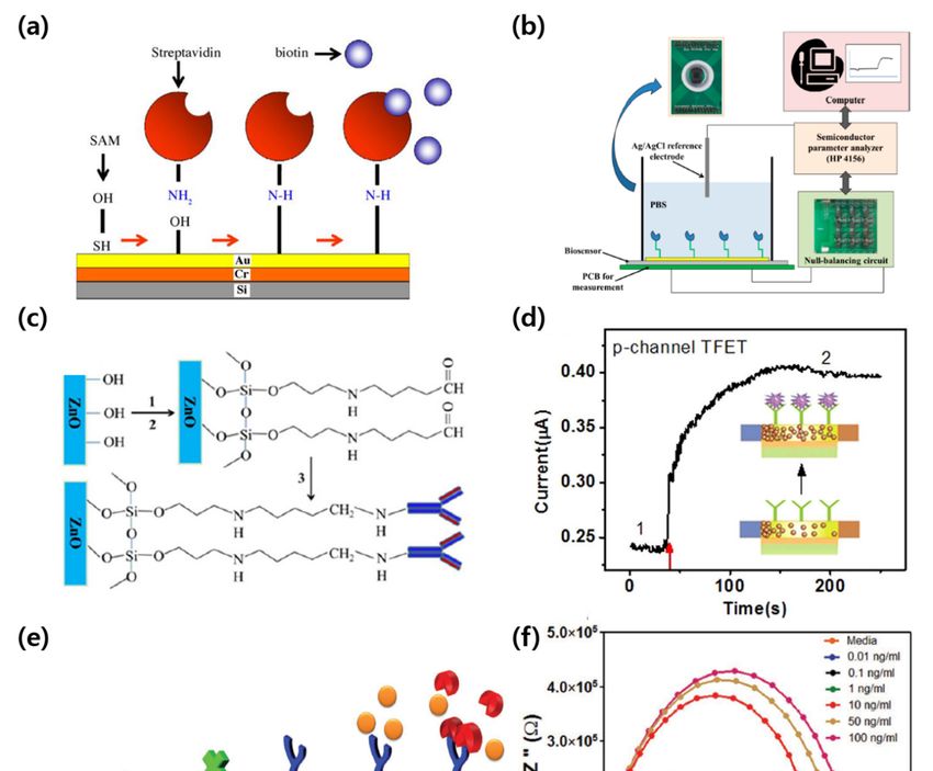
Micromachines 2021, 12, 565 3 of 17
Micromachines 2021, 12, x FOR PEER REVIEW 3 of 17
Figure
Figure1.1.SAM
SAMtreatment
treatmentononSiO
SiO2 2gate
gatedielectrics.
dielectrics.(a)
(a)Various
VariousSAMs
SAMsononthe
theSiO
SiO2 2surface
surface(adapted
(adaptedfrom
from[37]
[37]with
withpermission
permission
from the Royal Society of Chemistry). (b) Structure of a pSNT transistor with NTMS-treated SiO and
from the Royal Society of Chemistry). (b) Structure of a pSNT transistor with NTMS-treated SiO2 and the chemical
2 the chemical struc-
ture of NTMS (adapted from [38] with permission from John Wiley and Sons). (c) Transfer characteristics
structure of NTMS (adapted from [38] with permission from John Wiley and Sons). (c) Transfer characteristics of a poly(3-of a poly(3-
hexylthiophene) (P3HT) transistor before/after various silane-based SAM treatments on SiO2 (adapted from [39] with per-
hexylthiophene) (P3HT) transistor before/after various silane-based SAM treatments on SiO2 (adapted from [39] with
mission from the Royal Society of Chemistry). (d) BP transistor with ODTS- and APTES-treated SiO2 gate dielectric and
permission from the Royal Society of Chemistry). (d) BP transistor with ODTS- and APTES-treated SiO2 gate dielectric
the energy band diagram before/after each SAM treatment (adapted from [40] with permission from the American Chem-
andSociety).
ical the energy band diagram before/after each SAM treatment (adapted from [40] with permission from the American
Chemical Society).
2.2. SAM Treatment on Al2O3 Gate Dielectrics
2.2. SAM Treatment on Al2 O3 Gate Dielectrics
In addition to the SAM treatment on SiO2, many advances of SAM-treated Al2O3 have
In addition
been reported. to the
Jang SAM
et al. treatment
treated on SiO2 , many
the hydrophilic advances
surface of Al2Oof SAM-treated
3 with Al2 O3 have
various phosphonic
been reported. Jang et al. treated the hydrophilic surface
acid SAMs and compared the characteristics based on the alkyl of Al O with various phosphonic
2 3 chain length and func-
acid SAMs
tional and compared
end groups of the SAMsthe characteristics based
(Figure 2a) [41]. on the alkyl
The longer chain
the alkyl length
chain and functional
length, the more
end groups of the SAMs (Figure 2a) [41]. The longer the alkyl chain length,
hydrophobic the surface, resulting in greater contact angle characteristics. The character- the more
hydrophobic the surface, resulting in greater contact angle characteristics.
istics of phosphonic acid SAM according to functional end-groups were identified The charac-
as
teristics of phosphonic acid SAM according to functional end-groups
phosphonohexadecanoic acid (PHDA), 12-mercaptododecylphosphonic acid (MDPA), were identified as
phosphonohexadecanoic acid
12-pentafluorophenoxydodecylphosphonic(PHDA), 12-mercaptododecylphosphonic
acid (PFPA), acid
and (MDPA), 12-
11-hy-
pentafluorophenoxydodecylphosphonic
droxyundecylphosphonic acid (PFPA),
acid (HUPA). Among and 11-hydroxyundecylphosphonic
these phosphonic acid SAMs, only PFPA,
acid (HUPA).
which Amongfunctional
has a non-polar these phosphonic
end-group,acid SAMs, only
exhibited PFPA, which
hydrophobic has a similar
properties non-polar
to
functional end-group, exhibited hydrophobic properties similar to alkyl phosphate SAMs.
alkyl phosphate SAMs. It was established that PHDA, MDPA, and HUPA have high sur-
It was established that PHDA, MDPA, and HUPA have high surface energy character-
face energy characteristics because their functional end-groups are polar. Aghamoham-
istics because their functional end-groups are polar. Aghamohammadi et al. investi-
madi et al. investigated the relationship between the gate dielectric thickness and the
gated the relationship between the gate dielectric thickness and the threshold voltage
threshold voltage of n-octadecylphosphonic acid (ODPA)- and
of n-octadecylphosphonic acid (ODPA)- and 12,12,13,13,14,14,15,15,16,16,17,17,18,18,18-
12,12,13,13,14,14,15,15,16,16,17,17,18,18,18-pentadecylfluoro-octadecylphosphonic acid
pentadecylfluoro-octadecylphosphonic acid (FDPA)-treated Al O3 in DNTT transistors
(FDPA)-treated Al2O3 in DNTT transistors (Figure 2b) [42]. In the 2case of FDPA, when the
(Figure 2b) [42]. In the case of FDPA, when the Al2 O3 thickness increased, the threshold
Al2O3 thickness increased, the threshold voltage showed an inverse relationship with the
voltage showed an inverse relationship with the dielectric capacitance. In contrast, for the
dielectric capacitance. In contrast, for the ODPA-treated Al2O3, the threshold voltage was
ODPA-treated Al2 O3 , the threshold voltage was determined only by the SAM, regardless of
determined only by the SAM, regardless of the thickness of the Al2O3. Therefore, they
the thickness of the Al2 O3 . Therefore, they suggested that the shift in threshold voltage for
suggested that the shift in threshold voltage for the SAM-treated gate dielectric was re-
the SAM-treated gate dielectric was related not only to the dipole of the SAM material, but
lated not only to the dipole of the SAM material, but also to the interface between the SAM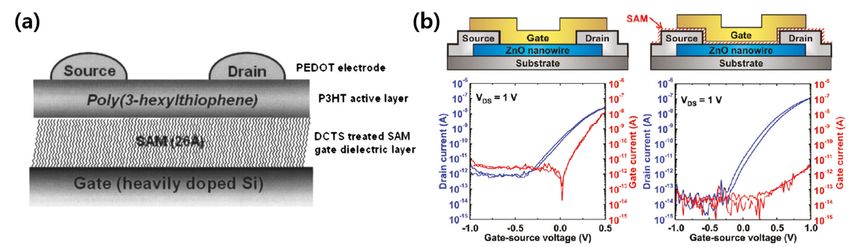
Micromachines 2021, 12, 565 4 of 17
Micromachines 2021, 12, x FOR PEER REVIEW 4 of 17
also to the interface between the SAM material and the semiconductor layer. Kawanago
material and thethe
et al. analyzed semiconductor
changes when layer. Kawanago et
ODTS-treated Alal.
2 Oanalyzed the changes
3 was applied when
as the gate ODTS-
dielectric
of an oxide
treated Al2Osemiconductor-based
3 was applied as the gate transistor (Figure
dielectric 2c) [43].
of an oxide After the ODTS treatment,
semiconductor-based as
transistor
the density
(Figure of the
2c) [43]. trapthe
After between the channel
ODTS treatment, asand
the the gateof
density dielectric
the trapdecreased,
between the the carrier
channel
mobility
and anddielectric
the gate on/off current ratio increased.
decreased, the carrierCai et al. used
mobility andan ODPA-treated
on/off Al2 O
current ratio 3 gate for
increased.
the et
Cai low-voltage
al. used anoperation of MoS2Al
ODPA-treated [44].
2O3 The
gategate leakage
for the current was
low-voltage significantly
operation of MoS reduced
2 [44].
by the
The gateODPA treatment
leakage current (Figure 2d).
was significantly reduced by the ODPA treatment (Figure 2d).
Figure
Figure 2.
2. SAM treatmenton
SAM treatment onAlAl 2O3 gate dielectrics. (a) Chemical structures of various phosphonic acid SAMs. [1: Hex-
2 O3 gate dielectrics. (a) Chemical structures of various phosphonic acid SAMs. [1: Hexylphos-
ylphosphonic acid (HPA), 2: dodecylphosphonic
phonic acid (HPA), 2: dodecylphosphonic acid (DDPA), acid 3:
(DDPA), 3: octadecylphosphonic
octadecylphosphonic acid
acid (ODPA), 4: (ODPA), 4: 16-phosphono-
16-phosphonohexadecanoic
hexadecanoic acid (PHDA), 5: 12-mercaptododecylphosphonic acid (MDPA), 6:
acid (PHDA), 5: 12-mercaptododecylphosphonic acid (MDPA), 6: 12-pentafluorophenoxydodecylphosphonic acid (PFPA), 7:12-pentafluorophe-
noxydodecylphosphonic acid (PFPA), 7: 11-hydroxyundecylphosphonic acid (HUPA)] (adapted from [41] with permis-
11-hydroxyundecylphosphonic acid (HUPA)] (adapted from [41] with permission from Springer Nature). (b) Schematic of a
sion from Springer Nature). (b) Schematic of a DNTT transistor to compare the effect of two phosphonic acid SAM treat-
DNTT transistor to compare the effect of two phosphonic acid SAM treatments for the thickness of Al2 O3 gate dielectrics
ments for the thickness of Al2O3 gate dielectrics (ODPA, FDPA) (adapted from [42] with permission from the American
(ODPA, FDPA)
Chemical (adapted
Society). from [42]
(c) Transfer with permission
characteristics from the
of an IGZO American
transistor Chemical
with Society).
and without ODTS(c) on
Transfer
Al2O3 characteristics
(adapted fromof an
[43]
IGZOpermission
with transistor with
fromandJohnwithout ODTS
Wiley and on Al
Sons). 2 OComparison
(d) 3 (adapted from [43]
of the with
gate permission
leakage from
current John
with or Wiley and
without theSons).
ODPA (d)treat-
Com-
parison
ment of 2the
of Al gate leakage
O3 (adapted fromcurrent withpermission
[44] with or withoutfrom
the ODPA treatment of Al2 O3 (adapted from [44] with permission from
AIP Publishing).
AIP Publishing).
2.3. SAM Treatment on HfO2 Gate Dielectrics
2.3. SAM Treatment on HfO2 Gate Dielectrics
As another high-k dielectric layer, HfO2 dielectric was applied by SAM treatments.
ActonAs et another high-k
al. showed thatdielectric layer, HfO
the performance of2 adielectric was applied
low-voltage OTFT can by be
SAM treatments.
controlled by
Acton et al. showed that the performance of a low-voltage OTFT can
adjusting the carbon chain length of the alkyl PA SAM on the HfO2 insulating layer (Fig- be controlled by
adjusting the carbon chain length of the alkyl PA SAM on
ure 3a) [45]. It was suggested that the high carrier mobility was determined the HfO insulating layer
2 by the balance
(Figure 3a)
between the[45].
SAMsItthat
wasexhibited
suggested that thethickness
sufficient high carrier
andmobility was determined
the disordered by the
SAMs to prevent
balanceeffects
adverse between the high-k
in the SAMs gate
that exhibited
dielectric. sufficient
Kim et al. thickness
introduced and the disordered
hydrophobic SAMs
properties
to prevent adverse effects in the high-k gate dielectric. Kim et al. introduced
on the hydrophilic HfO2 surface by incorporating OH groups through OTS, ODTS, and n- hydropho-
bic properties on the
dodecylphosphonic acidhydrophilic HfO2 3b)
(DDPA) (Figure surface
[46].by incorporating
With OH groups
this, they produced through
a poly-(2,5-
Micromachines 2021, 12, 565                                                                                                               5 of 17
Micromachines 2021, 12, x FOR PEER REVIEW                                                                                                5 of 17

                                   OTS, ODTS, and n-dodecylphosphonic acid (DDPA) (Figure 3b) [46]. With this, they
                                  bis(2-decyltetradecyl)-3-(3″,4′-difluoro-[2,2′:5′,2″-terthiophen]-5-yl)-6-(thiophen-2-yl)                 pyr-
                                   produced a poly-(2,5-bis(2-decyltetradecyl)-3-(3”,40 -difluoro-[2,20 :50 ,200 -terthiophen]-5-yl)-
                                  rolo [3,4-c] pyrrole-1,4-(2H,5H)-dione) (PDPP2DT-T2)-based organic transistor capable of
                                   6-(thiophen-2-yl) pyrrolo [3,4-c] pyrrole-1,4-(2H,5H)-dione) (PDPP2DT-T2)-based organic
                                  low voltage operation (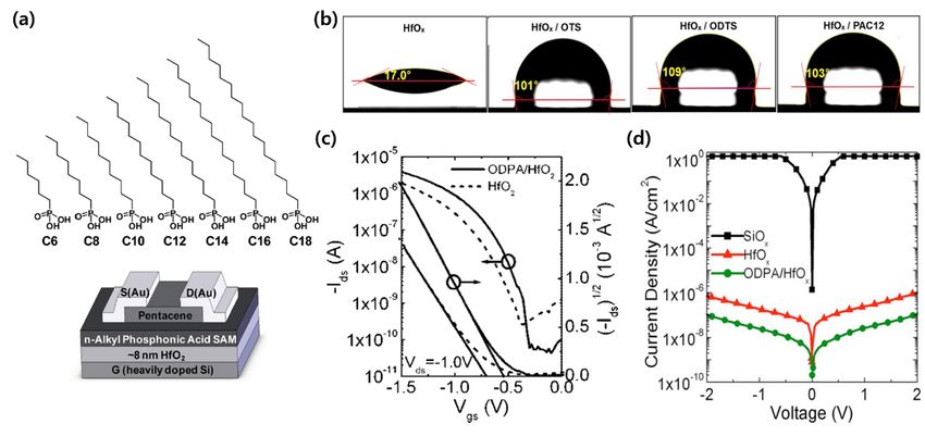
Micromachines 2021, 12, 565 6 of 17
Micromachines 2021, 12, x FOR PEER REVIEW 6 of 17
of low-voltage and low-power operation, even in organic devices. A solution-processed
(DCTS) SAM dielectric was
poly(3-hexylthiophene) demonstrated
(P3HT) (Figure 4a)
polymer transistor [50].aKälblein
using et al. prepared(DCTS)
docosyltrichlorosilane a top-
gate
SAM dielectric was demonstrated (Figure 4a) [50]. Kälblein et al. prepared a top-gate SAM
structure ZnO nanowire transistor in which ODPA, a phosphonic acid-based struc-
material,
ture ZnOwas applied
nanowire as the gate
transistor dielectric
in which ODPA,[51].a phosphonic
To confirm whether
acid-basedODPA
SAMismaterial,
effectivewas
as
aapplied
gate dielectric, thedielectric
as the gate electrical[51].
characteristics of the metal-semiconductor
To confirm whether ODPA is effective as FET a gate(MESFET)
dielectric,
structure without
the electrical the ODPAofgate
characteristics the dielectric and the metal-insulator-semiconductor
metal-semiconductor FET (MESFET) structure without FET
(MISFET) structure with the ODPA gate dielectric were compared (Figure
the ODPA gate dielectric and the metal-insulator-semiconductor FET (MISFET) structure 4b). The elec-
trical
with characteristics
the ODPA gateof the MESFET
dielectric structure without
were compared the ODPA
(Figure 4b). gate dielectric
The electrical and the
characteristics of
MISFET structure
the MESFET with the
structure ODPA
without thegate
ODPAdielectric were compared.
gate dielectric and the The
MISFETMESFET structure
structure with
without
the ODPA thegate
ODPA gate dielectric
dielectric exhibited
were compared. Thea high gate structure
MESFET leakage current
withoutflow. However,
the ODPA gate
the presence
dielectric of the ODPA
exhibited a highgate
gatedielectric greatlyflow.
leakage current reduced the gate
However, theleakage
presence current,
of the which
ODPA
improved the on/off
gate dielectric greatlycurrent
reduced ratio.
the Therefore,
gate leakage the dielectric
current, properties
which improved of the
ODPA were
on/off con-
current
firmed, and because of the thin thickness of the SAM, it was possible to operate
ratio. Therefore, the dielectric properties of ODPA were confirmed, and because of the thin the ZnO
nanowire
thicknesstransistor
of the SAM,at 1itV.
was possible to operate the ZnO nanowire transistor at 1 V.
Figure
Figure4.4.SAMs
SAMsasasgate
gatedielectrics.
dielectrics.(a)
(a)Schematic
SchematicofofP3HT
P3HTtransistor
transistorusing
usingdocosyltrichlorosilane
docosyltrichlorosilane(DCTS)
(DCTS)asasaagate
gatedielectric
dielectric
(adapted
(adaptedfrom
from[50]
[50]with
withpermission
permissionfromfrom AIP
AIP Publishing).
Publishing). (b)
(b)Comparison
Comparisonof ofthe
theelectrical
electricalcharacteristics
characteristicsin
inMISFET
MISFETand and
MESFET structures of ZnO nanowire FET with or without a SAM gate dielectric (adapted from [51] with permission
MESFET structures of ZnO nanowire FET with or without a SAM gate dielectric (adapted from [51] with permission from from
the American Chemical Society).
the American Chemical Society).
2.5.
2.5.Self-Assembled
Self-AssembledMonolayer
MonolayerFieldFieldEffect
EffectTransistor
Transistor (SAMFET)
(SAMFET)
AAself-aligned
self-alignedstructure
structureof ofSAMs
SAMsenabled
enabledtheirtheiroperation
operationas asaasemiconductor
semiconductoractive active
layer through the π–π overlap in the molecular packing. Cernetic
layer through the π–π overlap in the molecular packing. Cernetic et al. fabricated a et al. fabricated a p-type
SAMFET with (11-(5″′-(4-(methylthio)butyl)-[2,2′:5′,2″:5″,2″′-quaterthiophene]-5-yl)un-
p-type SAMFET with (11-(5000 -(4-(methylthio)butyl)-[2,20 :50 ,200 :500 ,2000 -quaterthiophene]-5-
decyl)phosphonic
yl)undecyl)phosphonic acid acid
(MTB4TC11)
(MTB4TC11) andand(12-(5″′-(4-(methylthio)butyl)-[2,2′:5′,2″:5″,2′′′-
(12-(5000 -(4-(methylthio)butyl)-[2,20 :50 ,200 :500 ,2000 -
quaterthiophene]-5-yl)
quaterthiophene]-5-yl) dodecyl) phosphonicacid
dodecyl) phosphonic acid (MTB4TC12),
(MTB4TC12), which which are are phosphonic
phosphonic
acid-based
acid-basedSAMsSAMs[52].[52].Figure
Figure5a 5ashows
showsthe theschematic
schematicofofthe thefabricated
fabricatedSAMFET.
SAMFET. They They
improved
improved thethe contact
contact characteristics
characteristics with with thetheAuAuelectrode
electrodeby byapplying
applyingmethylthiobutyl
methylthiobutyl as
as a functional
a functional terminal
terminal group.
group. In In addition,
addition, thethe bonding
bonding between
between the the
SAM SAMandand the elec-
the electrode
trode was strengthened
was strengthened through
through annealing,
annealing, so that
so that the the carrier
carrier mobility
mobility could
could be be increased
increased by
by more than 100-fold. By applying these optimized conditions,
more than 100-fold. By applying these optimized conditions, a SAMFET capable of low- a SAMFET capable of
low-voltage operation
voltage operation through
through a HfO a 2HfO
gate2 gate dielectric
dielectric was produced.
was produced. Zhao Zhao et al. imple-
et al. implemented
mented two organic
two organic invertersinverters using a SAMFET
using a SAMFET [53]. First,[53]. First,
after after fabricating
fabricating an ambipolar an ambipolar
transistor
transistor with a semiconducting
with a semiconducting SAM and SAM and a complementary
a complementary semiconductor,
semiconductor, they estab-a
they established
lished a CMOS-like
CMOS-like inverter inverter
with twowith two anti-ambipolar
anti-ambipolar transistors.transistors.
Second, aSecond,
CMOS ainverter
CMOS was in-
produced
verter by fabricating
was produced a benzothieno
by fabricating [3,2-b] [1][3,2-b]
a benzothieno benzothiophene (BTBT)-PA-based
[1]benzothiophene (BTBT)-PA- p-
type SAMFET
based and a 3,4,9,10-perylene
p-type SAMFET and a 3,4,9,10-perylene tetracarboxylic diimide
tetracarboxylic (PTCDI)-PA-based
diimide (PTCDI)-PA-based n-type
SAMFET
n-type (Figure
SAMFET 5b). They
(Figure presented
5b). They presentedthe possibility
the possibility of developing
of developing organic
organic circuits by
circuits
producing
by producing thethe
aforementioned
aforementioned SAM-based
SAM-based organic inverters
organic over
inverters a large
over areaarea
a large for the
for first
the
time.
first Gholamrezaie
time. Gholamrezaie et al.etsuggested
al. suggestedthatthat
semiconducting
semiconducting SAMs can can
SAMs be grown
be grown on organic
on or-
dielectrics
ganic and that
dielectrics andcharge transport
that charge is possible
transport even even
is possible at micrometer
at micrometerdistances [54]. They
distances [54].
also reported the use of a 4-bit code generator incorporating over
They also reported the use of a 4-bit code generator incorporating over 100 SAMFETs 100 SAMFETs (Figure 5c).
(Figure 5c). Andringa et al. reported the application of Fe(TPP)Cl as an NO receptor to a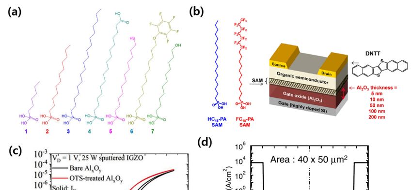
Micromachines 2021, 12, 565 7 of 17
Micromachines 2021, 12, x FOR PEER REVIEW 7 of 17
Andringa et al. reported the application of Fe(TPP)Cl as an NO receptor to a SAMFET and
used it as aand
SAMFET gas used
sensor
it (Figure
as a gas5d) [55].(Figure
sensor They suggested that asuggested
5d) [55]. They very thin that
SAMFET
a verychannel,
thin
approximately one molecule thick, is suitable for use as a sensor.
SAMFET channel, approximately one molecule thick, is suitable for use as a sensor.
Figure 5. SAMs
Figure 5. SAMsas as
semiconductor
semiconductorlayers.
layers.(a)
(a)Schematic
Schematic of
of aa SAMFET basedon
SAMFET based onphosphonic
phosphonicacidacidSAM
SAM (adapted
(adapted from
from [52][52]
with
with permission
permission from
from John
John Wiley
Wiley andSons).
and Sons).(b)
(b)Schematic
Schematic and
and illustration
illustration ofofaaSAMFET-based
SAMFET-basedCMOS CMOS inverter (adapted
inverter (adapted
from
from [53][53]
withwith permission
permission fromJohn
from JohnWiley
WileyandandSons).
Sons). (c)
(c) The
The output
output ofof aa 4-bit
4-bitcode
codegenerator
generatorincorporating
incorporating over 100100
over
SAMFETs. The red dotted line indicates the preprogrammed code (adapted from [54] with permission
SAMFETs. The red dotted line indicates the preprogrammed code (adapted from [54] with permission from the American from the American
Chemical Society). (d) Typical SAMFET transfer characteristic and the schematics of a SAM-based gas sensor (adapted
Chemical Society). (d) Typical SAMFET transfer characteristic and the schematics of a SAM-based gas sensor (adapted
from [55] with permission from Elsevier).
from [55] with permission from Elsevier).
3. SAMs as Dopants
3. SAMs as Dopants
In the second section, the effects of SAMs acting as dopants on the device’s properties
are In the second
introduced. Insection,
the last the effects
decade, of SAMssemiconductor
promising acting as dopants on the including
materials, device’s properties
transi-
are introduced. In the last decade, promising semiconductor materials,
tion metal dichalcogenides (TMDs) [56–60], oxides [61–65], and polymers [66–70], including transition
have
metal dichalcogenides
emerged (TMDs)semiconductors.
as next-generation [56–60], oxides [61–65],
However,andthe
polymers [66–70],doping
conventional have emerged
tech-
asniques
next-generation semiconductors.
(i.e., ion implantation) usedHowever, the conventional
in silicon-based doping
fabrications techniques
degrade (i.e., ion
and damage
implantation) used in silicon-based fabrications degrade and damage these semiconductors;
these semiconductors; thus, there is a need for the development of alternative methods to
thus, there
control theiselectrical
a need for the development
properties of alternative
of the semiconductors. Tomethods to control
meet these demands, theunusual
electrical
properties
SAM-based of doping
the semiconductors.
techniques have Tobeen
meetattempted
these demands,
[71–80].unusual
Owing to SAM-based
the ordereddoping
do-
techniques
main and large have area
beencoverage
attempted [71–80].
of SAMs, Owingand
uniform to controllable
the ordereddoping
domainwas andachieved.
large area
coverage
An expansiveof SAMs, uniform
overview and controllable
of SAM-based dopingdoping was achieved.
into oxides and TMDsAnisexpansive
presented overview
in this
ofsection.
SAM-based doping into oxides and TMDs is presented in this section.
3.1.
3.1.Doping
DopingEffects
Effectsof
of SAMs
SAMs in Oxide
Oxide Semiconductors
Semiconductors
InInrecent
recentyears,
years,the
the use
use of SAMs
SAMs as asaalayer
layerofofremote
remotedoping
doping material
material forfor prefabricated
prefabricated
transistors,
transistors, not asan
not as aninsulating
insulating film
film or aor a semiconductor,
semiconductor, hasattempted.
has been been attempted.
As an exam-As an
example of doping
ple of this this doping technique
technique of an SAMof anonSAM on oxide
a metal a metal oxide semiconductor,
semiconductor, Cai et al.
Cai et al. treated
treated
an IGZO an IGZO
surfacesurface
with ODTSwith ODTS
to form to aform a passivation
passivation layer (Figure
layer (Figure 6a), which
6a), which greatlygreatly
in-
creased the
increased thecarrier
carriermobility
mobility[79].
[79].InInaddition,
addition,without
withoutthethepassivation
passivationlayer, thethe
layer, device
device
significantlydeteriorated
significantly deteriorated after
after 1 year, whereas
whereasthe thedevice
devicecontaining
containing the passivation
the passivation layer
layer
maintained its performance after 1 year (Figure 6b). This indicates that the passivation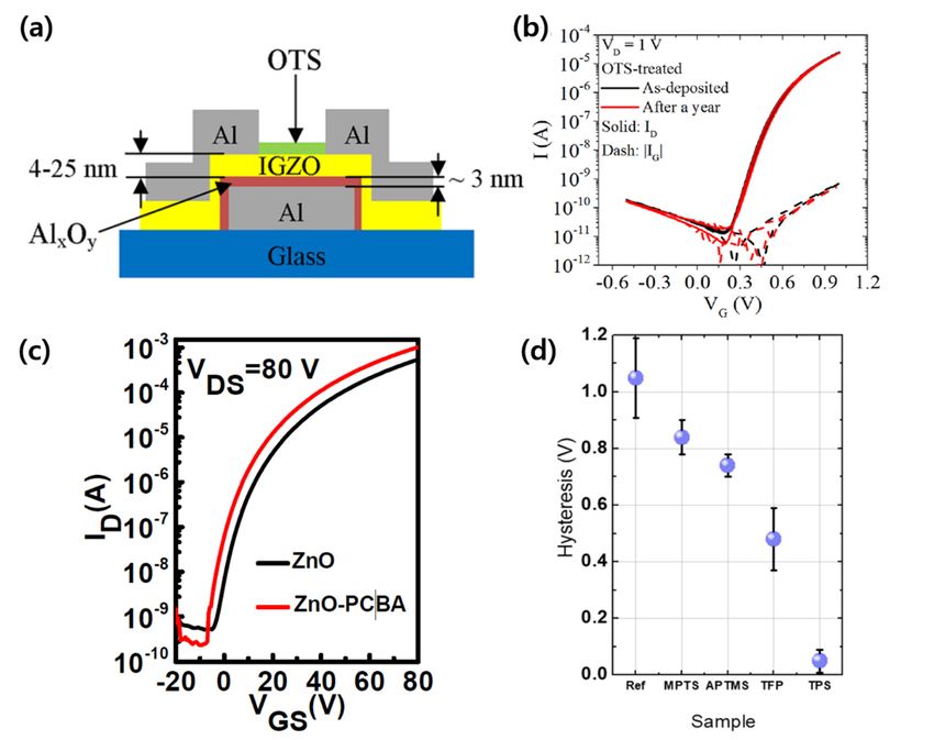
Micromachines
Micromachines 2021,2021, 12, x FOR PEER REVIEW
12, 565 88
ofof
1717
maintained its performance after 1 year (Figure 6b). This indicates that the passivation
layer introduced through the SAM treatment protected the device from oxygen derivatives
layer introduced through the SAM treatment protected the device from oxygen deriva-
from the air over an extended period. Wan et al. improved electron mobility and the
tives from the air over an extended period. Wan et al. improved electron mobility and the
on/off current ratio through the 4-chlorobenzoic acid (PCBA) treatment of ZnO transistors
on/off current ratio through the 4-chlorobenzoic acid (PCBA) treatment of ZnO transistors
(Figure 6c) [81]. They extracted the trap concentration from the electrical characteristics of a
(Figure 6c) [81]. They extracted the trap concentration from the electrical characteristics of
pristine ZnO transistor and a PCBA-treated ZnO transistor and found that it decreased by
a pristine ZnO transistor and a PCBA-treated ZnO transistor and found that it decreased
about 10-fold
by about after PCBA
10-fold treatment.
after PCBA Lee etLee
treatment. al. et
studied the surface
al. studied treatment
the surface of IGZO
treatment TFTs
of IGZO
with SAMs [78]. The results showed that by selecting a SAM with
TFTs with SAMs [78]. The results showed that by selecting a SAM with an appropriate an appropriate functional
group polarity
functional andpolarity
group alkyl chain length,
and alkyl thelength,
chain electron thetransport could becould
electron transport improved and the
be improved
hysteresis reduced (Figure 6d). In addition, it was shown that the
and the hysteresis reduced (Figure 6d). In addition, it was shown that the contact contact resistance canre-be
controlled by the alkyl chain length when using the same functional group.
sistance can be controlled by the alkyl chain length when using the same functional group. A similar result
wasAachieved by Xiao
similar result wasetachieved
al. for IGZO TFTset[75].
by Xiao al. forXiao
IGZOet al.TFTs
analyzed the effect
[75]. Xiao of passivating
et al. analyzed the
theeffect
surface of an IGZO TFT with triethoxysilane (TES)-based SAMs.
of passivating the surface of an IGZO TFT with triethoxysilane (TES)-based SAMs. In addition, three
types of TESs three
In addition, containing
types ofdifferent carbon different
TESs containing chain lengths,carbonnamely methyltriethoxysilane
chain lengths, namely methyl-
(MTES), octyltriethoxysilane
triethoxysilane (OTES), and oxtadecyltriethoxysilane
(MTES), octyltriethoxysilane (ODTES), were used to
(OTES), and oxtadecyltriethoxysilane
determine
(ODTES),the effect
were used oftothe alkyl chain
determine length
the effect of on
thethe semiconductor
alkyl chain length oncharacteristics.
the semiconductor As a
result, the longer the
characteristics. As aalkyl chain
result, thelength,
longer the
the more
alkyl improved
chain length, all the electrical characteristics,
more improved all the
such as carrier
electrical mobility and
characteristics, hysteresis.
such as carrier mobility and hysteresis.
Figure
Figure 6. SAMs
6. SAMs as dopants
as dopants in oxide
in oxide semiconductor-based
semiconductor-based transistors(a)
transistors (a)Schematic
Schematic of
of ODTS-treated
ODTS-treated IGZO
IGZOTFTTFT(adapted
(adapted
from [79] with permission from the American Chemical Society). (b) Transfer characteristics of IGZO TFT immediately
from [79] with permission from the American Chemical Society). (b) Transfer characteristics of IGZO TFT immediately after
after ODTS treatment and 1 year later (adapted from [79] with permission from the American Chemical Society). (c) Com-
ODTS treatment and 1 year later (adapted from [79] with permission from the American Chemical Society). (c) Comparison
parison of pristine ZnO TFT and PCBA-treated ZnO TFT transfer characteristics (adapted from [81] with permission from
of pristine
MDPI).ZnO TFT and PCBA-treated
(d) Hysteresis characteristics ZnO TFTTFT
of IGZO transfer characteristics
according (adapted
to SAM (adapted from
from [78][81] with
with permission
permission fromfrom MDPI).
the Amer-
(d) Hysteresis characteristics
ican Chemical Society). of IGZO TFT according to SAM (adapted from [78] with permission from the American
Chemical Society).
3.2. Electrical Doping Effect of SAMs in 2D Materials
The SAM doping techniques were attempted in 2D TMDs. Due to the atomically thin
nature of the TMDs, the SAM doping was more effective in improving device performance.
Kang et al. reported improved electrical properties for MoS2 and WSe2 transistors by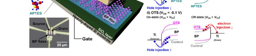
Micromachines 2021, 12, x FOR PEER REVIEW 9 of 17
3.2. Electrical Doping Effect of SAMs in 2D Materials
Micromachines 2021, 12, 565 9 of 17
The SAM doping techniques were attempted in 2D TMDs. Due to the atomically thin
nature of the TMDs, the SAM doping was more effective in improving device perfor-
mance. Kang et al. reported improved electrical properties for MoS2 and WSe2 transistors
by doping
doping withwith
ODTS ODTSandandAPTESAPTES SAM SAM materials
materials (Figure
(Figure 7a) [72].
7a) [72]. When When the MoS
the MoS 2 tran-
2 transistors
sistors were doped
were doped with APTES
with APTES and the andWSe the2WSe 2 transistors
transistors withwith
ODTS, ODTS,
the the field-effect
field-effect mo-
mobility
bility increased
increased by approximately
by approximately fivefold.fivefold. In contrast,
In contrast, when when
doping doping
the MoSthe MoS
2 2 transistor
transistor with
with
ODTS ODTS
and and the WSe
the WSe 2 2 transistor
transistor withwith APTES,
APTES, the
the field-effect
field-effect mobility
mobility deteriorated.
deteriorated. AsAs
ODTS
ODTS and andAPTES
APTESexhibited
exhibitedp-doped
p-doped and and n-doped
n-doped effects, the the
effects, n-type
n-typeMoS2MoS could 2 be
could im- be
proved by APTES doping, and the p-type WSe could be
improved by APTES doping, and the p-type WSe2 could be improved by ODTS doping.
2 improved by ODTS doping. They
also
Theysuggested that thethat
also suggested p-doping effect of effect
the p-doping the ODTS-doped WSe2 transistor
of the ODTS-doped WSe2 was owing was
transistor to
the functional group of the ODTS [73]. Due to the positive charges
owing to the functional group of the ODTS [73]. Due to the positive charges of the of the methyl functional
groups
methyl (-CH 3) in ODTS,
functional groups the(-CH
electrons in WSe2the
3 ) in ODTS, areelectrons
attracted in to WSe
the junction with ODTS,
2 are attracted to the
which
junctionleads
withtoODTS,
a decrease
whichinleads
the concentration
to a decrease in ofthe
electrons in the WSe
concentration 2 channel
of electrons inandthe aWSe
p- 2
doping
channeleffect
and a(Figure
p-doping 7b).effect
Hasnain et al.7b).
(Figure studied
Hasnainthe doping effect of
et al. studied the (3-aminopropyl)tri-
doping effect of (3-
methoxysilane (APTMS) in ReSe
aminopropyl)trimethoxysilane 2 transistors
(APTMS) in ReSewith n-type characteristics
2 transistors with n-typeas a function ofas
characteristics
the
a function of the APTMS concentration (Figure 7c–e) [74]. They suggested thatconcentra-
APTMS concentration (Figure 7c–e) [74]. They suggested that the electron the electron
tion in the ReSein
concentration 2 channel
the ReSeincreased
2 channelbecauseincreased of the negative
because charges
of the of the
negative amineof
charges functional
the amine
groups (-NH
functional 2) of APTMS
groups (-NH2 ) of atAPTMS
the interfaceat the between
interface APTMS
betweenand ReSeand
APTMS 2. As a result,
ReSe 2 . As the n-
a result,
doping effect of
the n-doping APTMS
effect reduced
of APTMS the effective
reduced barrierbarrier
the effective heightheight
between ReSe2 and
between ReSethe elec-
2 and the
trode, andand
electrode, the the
threshold
threshold voltage
voltage shifted
shifted in in
thethenegative
negative direction.
direction. After
Afterdoping
dopingwith with
APTMS, these effects increased
increased the the photoresponsivity
photoresponsivity for forall
allwavelength
wavelengthbands,bands,not notonly
onlyin
in terms
terms of of electrical
electrical characteristics,
characteristics, but but also
also ininterms
termsofofthe thephotoresponsive
photoresponsiveproperties.
properties.
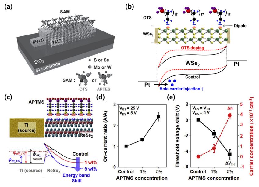
Figure 7. SAMs as dopants in TMD-based transistors. (a) Schematic of a SAM-doped TMD-based transistor (adapted
from [72] with permission from John Wiley and Sons). (b) Energy band diagram of a WSe2 transistor before/after ODTS
doping (adapted from [73] with permission from the American Chemical Society). (c) Charge polarity at the APTMS-ReSe2
interface and the change of energy band diagram after the doping of an ReSe2 transistor by APTMS concentration (1 and
5 wt%). Comparison of (d) on-current ratio, (e) threshold voltage shift, and carrier concentration according to APTMS
concentration (adapted from [74] with permission from Elsevier).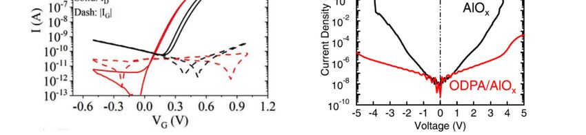
Micromachines 2021, 12, 565                                                                                            10 of 17

                              4. Biosensor Linkers Based on SAMs
                                   Finally, we revisit the recent advances and studies in biosensors that use SAM-based
                              linkers. Recent viral diseases and pandemics have generated interest in various types
                              of sensors, such as electrochemical impedance spectroscopy (EIS) [82–84] and field-effect
                              biosensors (BioFETs) [85–89]. These devices can provide warnings on a patient’s dangerous
                              condition or offer daily monitoring information. Biosensors should exhibit crucial functions,
                              including fast detection and response [90], robust operation [91], and the detection of low-
                              concentration targets [92], for reliable detection systems. To realize these functions, a linker
                              with an ordered domain should be located between the active layer and the analytes to
                              anchor the analytes (i.e., target antibodies and enzymes). As molecular assemblies allow
                              SAMs to be tightly packed and oriented on the active layer, a dense domain of analytes can
                              be formed. In this section, we provide an overview of biosensors for antigen and biomarker
                              detection enhanced by using SAM-based linkers.
                                   Kim et al. studied an extended gate FET (EGFET)-based biosensor for detecting
                              streptavidin–biotin protein complexes [93]. The sequence of immobilization of streptavidin
                              to the gate electrode is shown in Figure 8a. They used a C11-oligo(ethylene glycol)-
                              terminated (OEG) thiol SAM with thiol and hydroxyl groups to immobilize streptavidin
                              (SPV) on the Au gate electrode. The OEG thiol SAM head group thiols, was bonded to
                              the Au gate electrode to form a hydroxyl group on the surface. Then, streptavidin was
                              immobilized by combining the amine group of streptavidin with the surface’s hydroxyl
                              group. Similarly, Lee et al. demonstrated a biosensor based on a high electron mobility
                              transistor (HEMT) for C-reactive protein (CRP) detection by immobilizing the antibody on
                              the gate [94]. To immobilize the receptor, CRP, a carboxyl group was first formed on the
                              gate surface with 11-mercaptoundecanoic acid(11-MUA), and then a stable amine-reactive
                              product was formed with N-(3-dimethylaminopropyl)-N0 -ethylcarbodiimide hydrochlo-
                              ride (EDC) and N-hydroxysuccinimide (NHS). Then, CRP-antibody immobilization was
                              completed. Figure 8b shows the AlGaN/GaN HEMT-based biosensor configuration for
                              CRP detection. They detected CRP by measuring not only the change in drain current
                              but also the change in the output voltage using a null-balancing circuit. In addition to
                              immobilizing the receptor on the gate electrode, a method of immobilizing the receptor on
                              the channel layer has also been reported. Liu et al. immobilized uricase on a ZnO nanowire
                              channel to fabricate a sensor that detects uric acid [88]. Figure 8c shows the process of im-
                              mobilizing uricase. First, the hydroxyl group on the ZnO nanowire surface was converted
                              into an amine group by silane-based APTES treatment. Then, the surface modification was
                              completed by linking the uricase and the amine group through glutaraldehyde. Gao et al.
                              demonstrated a tunnel field-effect transistor (TFET)-based biosensor capable of detecting
                              CYFRA21-1, a lung cancer biomarker [85]. They first formed amine groups on the Si
                              nanowire channel by APTES treatment. Subsequently, the amine group on the Si nanowire
                              surface was reacted with glutaraldehyde, and then the CYFRA21-1 antibody was immobi-
                              lized. When the CYFRA21-1 antigen and antibody were combined, the electrical properties
                              acting on the channel region was changed, influenced by the polarity of the biomolecule.
                              The energy band structure of the TFET and the tunneling current were also modulated
                              (Figure 8d). As a result, the presence of CYFRA21-1 antigen could be detected through
                              the change of the current of the TFET. Shin et al. demonstrated a biosensor for detecting
                              biomarkers related to liver health based on EIS [95]. Starting with the SAM treatment, the
                              antibody’s binding process to the Au electrode is shown in Figure 8e. The Au electrode
                              was treated with 11-MUA SAM, and NHS ester was formed through EDC/NHS. Then,
                              SPV was immobilized by reacting the surface with the amine group of SPV. Finally, it was
                              completed by immobilizing biotinylated antibodies (biot-Abs) to SPV. The detection of the
                              target in the fabricated sensor was achieved through the change in impedance as shown in
                              Figure 8f.
Then, SPV was immobilized by reacting the surface with the amine group of SPV. Finally,
it was completed by immobilizing biotinylated antibodies (biot-Abs) to SPV. The detec-
Micromachines 2021, 12, 565 11 of 17
tion of the target in the fabricated sensor was achieved through the change in impedance
as shown in Figure 8f.
Figure 8. SAMs as a linker in biosensors. (a) Schematic of the immobilization sequence of streptavidin and the interaction
between streptavidin
between streptavidin and
and biotin
biotin (adapted
(adaptedfrom
from[93]
[93]with
withpermission
permissionfromfromElsevier).
Elsevier).(b)(b)
Measurement
Measurement setup to detect
setup C-
to detect
reactive protein
C-reactive protein(adapted
(adaptedfrom
from[94]
[94]with
withpermission
permissionfrom
fromMDPI).
MDPI).(c)(c)Immobilization
Immobilization of of uricase
uricase onto
onto the
the ZnO
ZnO NW surface
NW surface
via the crosslinking surface modification method: (1) 2% APTES in ethanol; (2) 25 wt% GAD; (3) 5μL uricase (5 units/mL)
via the crosslinking surface modification method: (1) 2% APTES in ethanol; (2) 25 wt% GAD; (3) 5µL uricase (5 units/mL)
(adapted from [88] with permission from Elsevier). (d) Electrical characteristics of an SiNW-TFET based biosensor detect-
(adapted from [88] with permission from Elsevier). (d) Electrical characteristics of an SiNW-TFET based biosensor detecting
ing CYFRA21-1 (adapted from [85] with permission from Springer Nature). (e) Illustration of immobilizing antibodies
CYFRA21-1 (adapted fromand
onto the microelectrodes [85]reacting
with permission from Springer
with antigens (adaptedNature).
from [95](e)with
Illustration of immobilizing
permission antibodies
from John Wiley onto the
and Sons). (f)
microelectrodes and reacting with antigens (adapted from [95] with permission from John Wiley and Sons).
Nyquist plots for different standard human albumin concentrations. Media refers to the treatment of cell culture media to (f) Nyquist
plots for the
prevent different standard
nonspecific human
binding albumin (adapted
of proteins concentrations. Media
from [95] withrefers to the treatment
permission from JohnofWiley
cell culture media to prevent
and Sons).
the nonspecific binding of proteins (adapted from [95] with permission from John Wiley and Sons).
5. Summary
We first revisited examples of using SAM for the surface treatment of oxide gate
dielectrics in electronics. Oxide dielectrics had problems due to charge traps caused by
hydroxyl groups on the surface and problems with leakage current flowing in high-kMicromachines 2021, 12, 565 12 of 17
dielectrics such as Al2 O3 and HfO2 . These problems in the oxide dielectric were addressed
by the SAM; the SAMs reacting with the hydroxyl groups on the dielectric surface were
treated. The increased hydrophobicity can improve device performance because it mini-
mizes the absorption of oxygen or water molecules that result in poor device stability and
performance degradation. As the SAM treatment reduced the charge trap by allowing the
hydrophilic surface to become hydrophobic. The decrease in trap density led to improved
electrical characteristics such as high on/off current ratio and the enhanced mobility of
the devices. Besides, several researchers have experimentally proven that there is also an
effect by the carbon chain of SAM. This is because the longer the carbon chain length is, the
better the SAM molecules can be ordered and the more hydrophobic the surface is.
Interestingly, SAMs themselves are also used as gate dielectrics or semiconductor
layers. Table 1 shows examples of applying SAMs to the gate dielectric surface treatment
and examples of using a SAM itself as a gate dielectric. The possibility of applying a
molecularly thin SAM as a gate dielectric mean that the device can be operated with
low voltage. Based on these research results, this has been demonstrated for SAM gate
dielectric- and SAMFET-based functional circuit-levels such as NANDs, ring oscillators,
and code generators. This shows that SAMs have great potential in electronics.
Table 1. Various types of self-assembled monolayers (SAMs) for gate dielectrics.
Bottom Operating
Name Type Head Group End Group Method Ref.
Layer Voltage
Trimethoxysilane Amine SiO2
NTMS Silane Spin-coating 80 V [38]
(-Si(OCH3 )3 ) (-NH2 ) (285 nm)
Triethoxysilane Amine SiO2
APTES Silane Dipping −40 V [40]
(-Si(OC2 H5 )3 ) (-NH2 ) (285 nm)
Trichlorosilane Methyl SiO2
OTS Silane Dipping −40 V [40]
(-SiCl3 ) (-CH3 ) (285 nm)
Trichlorosilane Phenyl SiO2
PTS Silane N/A −60 V [39]
(-SiCl3 ) (-C6 H5 ) (N/A)
Trichlorosilane Methyl SiO2
MTS Silane N/A −60 V [39]
(-SiCl3 ) (-CH3 ) (N/A)
Trichlorosilane Methyl SiO2
ODTS Silane Dipping −80 V [37]
(-SiCl3 ) (-CH3 ) (300 nm)
Triethoxysilane Trifluoromethyl SiO2
FDTS Silane Dipping −80 V [37]
(-Si(OC2 H5 )3 ) (-CF3 ) (300 nm)
Phosphonic Methyl Al2 O3
HPA Phosphonic acid Spin-coating −4 V [41]
(-PO(OH)2 ) (-CH3 ) (N/A)
Phosphonic Methyl Al2 O3
DDPA Phosphonic acid Spin-coating −4 V [41]
(-PO(OH)2 ) (-CH3 ) (N/A)
Phosphonic Carboxyl Al2 O3
PHDA Phosphonic acid Spin-coating −4 V [41]
(-PO(OH)2 ) (-COOH) (N/A)
Phosphonic Thiol Al2 O3
MDPA Phosphonic acid Spin-coating −4 V [41]
(-PO(OH)2 ) (-SH) (N/A)
Phosphonic Al2 O3
PFPA Phosphonic acid Pentafluorophenoxy Spin-coating −4 V [41]
(-PO(OH)2 ) (N/A)
Phosphonic Hydroxyl Al2 O3
HUPA Phosphonic acid Spin-coating −4 V [41]
(-PO(OH)2 ) (-OH) (N/A)
Phosphonic Trifluoromethyl Al2 O3
FDPA Phosphonic acid Dipping −2.5 V [42]
(-PO(OH)2 ) (-CF3 ) (5 nm)
Phosphonic Methyl Al2 O3
ODPA Phosphonic acid Dipping −2.5 V [42]
(-PO(OH)2 ) (-CH3 ) (5 nm)
Phosphonic Methyl
ODPA Phosphonic acid Dipping X 1.5 V [51]
(-PO(OH)2 ) (-CH3 )
Trichlorosilane Phenyl Vapor-phase
PhO-OTS Silane X −2.1 V [49]
(-SiCl3 ) (-C6 H5 ) deposition
Trichlorosilane Methyl
DCTS Silane Dipping X -2 V [50]
(-SiCl3 ) (-CH3 )Micromachines 2021, 12, 565 13 of 17
The utility of SAMs is not limited to basic elements of devices such as gate dielectrics
and semiconductors, but is also used as a dopant for devices. TMDs and oxide semicon-
ductors, emerging as next-generation semiconductor materials, have difficulty applying
the ion implantation process for doping conventional silicon semiconductors. As an alter-
native to the conventional doping method, which is difficult to apply, studies have been
conducted to provide a doping effect by placing a SAM on a fabricated device. We have
summarized examples of doping attempts using SAM in Table 2. The doping effect in oxide
semiconductors and TMDs is slightly different. In oxide semiconductors, the hydroxyl
group acting as a trap on the surface of the semiconductor layer decreases through reaction
with the head group of the SAM, thereby eliminating the trapping sites and increasing the
number of carriers in the channel, thereby improving the device performance [78]. On the
other hand, in TMDs, the characteristics of the TMD-based transistor are modulated due to
the effect of the tail group of the SAM facing the semiconductor layer, and the dipole of the
tail group applies an electric field to the channel [71].
Table 2. Self-assembled monolayers (SAMs) used as a dopant.
Name Type Head Group End Group Method Bottom Layer Doping Type Ref.
Trimethoxysilane Methyl
ODTS Silane Spin-coating Graphene P-type [71]
(-Si(OCH3 )3 ) (-CH3 )
Trichlorosilane Methyl [72,
ODTS Silane Dipping WSe2 P-type
(-SiCl3 ) (-CH3 ) 73]
Trichlorosilane Methyl
ODTS Silane Spin-coating IGZO N-type [79]
(-SiCl3 ) (-CH3 )
Triethoxysilane Methyl Vapor-phase [76,
OTES Silane ITZO N-type
(-Si(OC2 H5 )3 ) (-CH3 ) deposition 77]
Triethoxysilane Amine
APTES Silane Dipping MoS2 N-type [72]
(-Si(OC2 H5 )3 ) (-NH2 )-
Trimethoxysilane Amine
APTMS Silane Dipping RSe2 N-type [74]
(-Si(OCH3 )3 ) (-NH2 )-
Finally, we dealt with the use of SAMs as a linker in biosensors. In biosensors, it is
necessary to have selectivity for the specific target to be detected, such as an antigen, and the
ability to detect if even a small concentration of the target is present is important. Therefore,
it is necessary to allow the maximum interaction between the target and the receptor to
occur. As a method, there is alignment by immobilizing receptors such as antibodies in a
specific direction. However, since not all receptors can be directly immobilized on various
substrates, SAMs are widely applied to connect and immobilize the substrate and the
receptor as a linker.
As there are many advantages, shown through various examples, of using SAMs,
further advances in electronics will be in progress. SAM-based electronic devices have
the following merits and directions for future research: (1) low-cost, (2) device flexibility,
(3) work-function modification, and (4) device stability enhancement. Owing to the solution
processability of SAMs, the SAM-based device process can be performed through simple
spin-coating or printing, which reduces the fabrication process complexity, and thus lowers
the cost. Furthermore, the low thermal budget of the SAM-based process enhances the
compatibility with flexible substrates (i.e., polyimide and polyethylene terephthalate).
These merits provide great ease in implementing flexible devices such as communication
devices and sensors [96,97]. In addition to the fabrication processing aspect, SAMs enable
the contribution towards device aspects. The work function modification can be achieved
by SAM surface treatment due to its molecularly thin thickness and assembly reaction.
This property ensures that the work function of the electrodes matches what can provide
the desired energy band junction for each device [98,99]. The SAMs also improve the
device stability. The SAM can control surface properties into hydrophobicity, minimizing
the absorption of oxygen or water molecules that act as charge trap sites. There are still
difficulties such as the improvement of the integration process, miniaturization, and patternMicromachines 2021, 12, 565 14 of 17
refinement in SAM-based electronics. However, the advantages and possibilities of the
aforementioned SAMs are expected to lead to the next generation of electronic devices.
Author Contributions: S.K. performed the literature research and analysis and wrote the paper. H.Y.
initiated and supervised the work and wrote the paper. All authors have read and agreed to the
published version of the manuscript.
Funding: This research was supported by a National Research Foundation of Korea (NRF) grant
funded by the Korean Government (MSIT) (NRF-2020R1A2C1101647 and NRF-2020M3A9E4104385).
Conflicts of Interest: The authors declare no conflict of interest.
References
1. Fox, H.; Zisman, W. The spreading of liquids on low energy surfaces. I. polytetrafluoroethylene. J. Colloid Sci. 1950, 5, 514–531.
[CrossRef]
2. Bain, C.D.; Whitesides, G.M. Modeling organic surfaces with self-assembled monolayers. Angew. Chem. 1989, 101, 522–528.
[CrossRef]
3. Bigelow, W.; Pickett, D.; Zisman, W. Oleophobic monolayers: I. Films adsorbed from solution in non-polar liquids. J. Colloid Sci.
1946, 1, 513–538. [CrossRef]
4. Klauk, H. Organic thin-film transistors. Chem. Soc. Rev. 2010, 39, 2643–2666. [CrossRef] [PubMed]
5. Horowitz, G.; Fichou, D.; Peng, X.; Garnier, F. Thin-film transistors based on alpha-conjugated oligomers. Synth. Met. 1991, 41,
1127–1130. [CrossRef]
6. Haddon, R.; Perel, A.; Morris, R.; Palstra, T.; Hebard, A.; Fleming, R.M. C60 thin film transistors. Appl. Phys. Lett. 1995, 67,
121–123. [CrossRef]
7. Torsi, L.; Dodabalapur, A.; Katz, H. An analytical model for short-channel organic thin-film transistors. J. Appl. Phys. 1995, 78,
1088–1093. [CrossRef]
8. Peng, X.; Horowitz, G.; Fichou, D.; Garnier, F. All-organic thin-film transistors made of alpha-sexithienyl semiconducting and
various polymeric insulating layers. Appl. Phys. Lett. 1990, 57, 2013–2015. [CrossRef]
9. Kim, J.H.; Hong, S.H.; Seong, K.D.; Seo, S. Fabrication of Organic Thin-Film Transistors on Three-Dimensional Substrates Using
Free-Standing Polymeric Masks Based on Soft Lithography. Adv. Funct. Mater. 2014, 24, 2404–2408. [CrossRef]
10. Uno, M.; Isahaya, N.; Cha, B.-S.; Omori, M.; Yamamura, A.; Matsui, H.; Kudo, M.; Tanaka, Y.; Kanaoka, Y.; Ito, M.; et al.
High-Yield, Highly Uniform Solution-Processed Organic Transistors Integrated into Flexible Organic Circuits. Adv. Electron.
Mater. 2017, 3, 1600410. [CrossRef]
11. Choi, H.H.; Yi, H.T.; Tsurumi, J.; Kim, J.J.; Briseno, A.L.; Watanabe, S.; Takeya, J.; Cho, K.; Podzorov, V. A large anisotropic
enhancement of the charge carrier mobility of flexible organic transistors with strain: A Hall effect and Raman study. Adv. Sci.
2020, 7, 1901824. [CrossRef]
12. Min, H.; Kang, B.; Shin, Y.S.; Kim, B.; Lee, S.W.; Cho, J.H. Transparent and colorless polyimides containing multiple trifluoromethyl
groups as gate insulators for flexible organic transistors with superior electrical stability. ACS Appl. Mater. Interfaces 2020, 12,
18739–18747. [CrossRef]
13. Kim, J.-H.; Liang, Y.; Seo, S. Patchable thin-film strain gauges based on pentacene transistors. Org. Electron. 2015, 26, 355–358.
[CrossRef]
14. Bischak, C.G.; Flagg, L.Q.; Ginger, D.S. Ion Exchange Gels Allow Organic Electrochemical Transistor Operation with Hydrophobic
Polymers in Aqueous Solution. Adv. Mater. 2020, 32, 2002610. [CrossRef]
15. Yoo, H.; Choi, H.H.; Shin, T.J.; Rim, T.; Cho, K.; Jung, S.; Kim, J.J. Self-Assembled, Millimeter-Sized TIPS-Pentacene Spherulites
Grown on Partially Crosslinked Polymer Gate Dielectric. Adv. Funct. Mater. 2015, 25, 3658–3665. [CrossRef]
16. Choi, C.G.; Bae, B.S. Effects of Hydroxyl Groups in Gate Dielectrics on the Hysteresis of Organic Thin Film Transistors. Electrochem.
Solid State Lett. 2007, 10. [CrossRef]
17. Gu, G.; Kane, M.G. Moisture induced electron traps and hysteresis in pentacene-based organic thin-film transistors. Appl. Phys.
Lett. 2008, 92. [CrossRef]
18. Lee, S.; Koo, B.; Shin, J.; Lee, E.; Park, H.; Kim, H. Effects of hydroxyl groups in polymeric dielectrics on organic transistor
performance. Appl. Phys. Lett. 2006, 88. [CrossRef]
19. Zhang, Y.; Ziegler, D.; Salmeron, M. Charge trapping states at the SiO2–oligothiophene monolayer interface in field effect
transistors studied by Kelvin probe force microscopy. ACS Nano 2013, 7, 8258–8265. [CrossRef]
20. Mathijssen, S.G.; Kemerink, M.; Sharma, A.; Cölle, M.; Bobbert, P.A.; Janssen, R.A.; de Leeuw, D.M. Charge Trapping at the
Dielectric of Organic Transistors Visualized in Real Time and Space. Adv. Mater. 2008, 20, 975–979. [CrossRef]
21. Chua, L.-L.; Zaumseil, J.; Chang, J.-F.; Ou, E.C.-W.; Ho, P.K.-H.; Sirringhaus, H.; Friend, R.H. General observation of n-type
field-effect behaviour in organic semiconductors. Nature 2005, 434, 194–199. [CrossRef] [PubMed]
22. McLean, F.B.; Boesch, H.E.; McGarrity, J.M.; Oswald, R.B. Rapid annealing and charge injection in Al2 O3 MIS capacitors. IEEE
Trans. Nucl. Sci. 1974, 21, 47–55. [CrossRef]
23. Zaininger, K.; Waxman, A. Radiation resistance of Al2 O3 MOS devices. IEEE Trans. Electron. Devices 1969, 16, 333–338. [CrossRef]You can also read