Short-wave infrared organic phototransistors with strong infrared-absorbing polytriarylamine by electron-transfer doping - Nature
←
→
Page content transcription
If your browser does not render page correctly, please read the page content below
www.nature.com/npjflexelectron

                  ARTICLE                 OPEN

                  Short-wave infrared organic phototransistors with strong
                  infrared-absorbing polytriarylamine by electron-transfer
                  doping
                                                                                          1✉
                  Chulyeon Lee1, Hwajeong Kim1,2 and Youngkyoo Kim

                      Short-wavelength infrared (SWIR) sensors have attracted keen attention due to the increasing necessity in a variety of scientific and
                      industrial applications, including biomedical and information technology fields. Because conventional SWIR sensors are made of
                      inorganic materials with rigid and brittle characteristics, organic materials with a discrete SWIR absorption are required for flexible
                      SWIR sensors in the flexible electronics era. Here, we demonstrate that a polytriarylamine, poly[N,N′-bis(4-butylphenyl)-N,N′-bis
                      (phenyl)benzidine] (PolyTPD), can absorb almost full range of SWIR wavelength (λ = 1000–3200 nm) after 48 h doping with tris
                      (pentafluorophenyl)borane (BCF). The spectroscopic characterization disclosed that an electron transfer from PolyTPD to BCF
                      created a new low energy level (gap) state leading to the SWIR absorption in the BCF-doped PolyTPD complexes. Organic
                      phototransistors (OPTRs) with the BCF-doped PolyTPD films as a gate-sensing layer could detect the SWIR light with a reasonable
                      photoresponsivity of ~538 mA W−1 (λ = 1500 nm), ~541 mA W−1 (λ = 2000 nm), and ~222 mA W−1 (λ = 3000 nm). The present
1234567890():,;

                      breakthrough SWIR-OPTR technology can pave a way for further advances in SWIR-absorbing organic materials and flexible SWIR
                      sensors.
                      npj Flexible Electronics (2021)5:10 ; https://doi.org/10.1038/s41528-021-00105-z

                  INTRODUCTION                                                                             two approaches: (1) covalent bonding approach by combining atoms
                  Infrared (IR), which is invisible to human eyes, has been widely                         and/or functional groups with largely different energy levels (i.e.,
                  used for various applications, such as optical communication,                            electron-donating and electron-accepting groups), and (2) doping
                  night vision, light detection and ranging, thermal imaging                               approach by forming new energy levels (gap states) via introduction
                  (temperature monitoring), IR spectroscopy, biomedical imaging,                           of chemical and/or physical dopants28,29. To date, very limited
                  etc.1–10. According to the wavelength (λ) of IR, the IR range can be                     number of IR-absorbing organic materials have been reported by the
                  further divided into five categories: near-infrared (NIR,                                 covalent bonding approach and their IR absorption range was below
                  λ = 0.75–1.4 μm), short-wavelength infrared (SWIR, λ = 1.4–3 μm),                        λ = 1800 nm (NIR but very small part of SWIR; see Supplementary
                  mid-wavelength infrared (MWIR, λ = 3–8 μm), long-wavelength                              Table 1)30–32. In contrast, the doping approach delivered extremely
                  infrared (LWIR, λ = 8–15 μm), and far infrared (FIR, λ =                                 shifted IR absorption up to λ = 2000 nm, which is supported by well-
                  15–1000 μm)11. To date, the detection of IR could be possible                            known conducting polymers, such as poly(3,4-ethylenedioxythio-
                  using sensors based on inorganic materials, for example, silicon                         phene):poly(styrenesulfonate) (PEDOT:PSS) and polyaniline:camphor-
                  and germanium for NIR, indium gallium arsenide (InGaAs) for NIR                          sulfonic acid (PANI:CSA)33,34. The PEDOT:PSS and PANI:CSA polymers
                  and SWIR, indium antimonide (InSb) and mercury cadmium                                   have been reported to exhibit a broad range of IR absorption from
                  telluride (HgCdTe) for MWIR and LWIR, platinum silicide (PtSi; or                        λ = ca. 1000 nm to λ = ca. 2000 nm35,36. However, these doped
                  microbolometers) for LWIR, etc.12–15. In particular, SWIR has                            polymers could not attract much attention as an IR sensor because of
                  become one of the important IR categories because it can detect                          their predominant applications for electrodes and/or interfacial
                  further things underneath the surface of objects thanks to its                           charge transport layers thanks to the versatile electrical conductiv-
                  capability of penetration deeper than a shorter wavelength light                         ity37–40. Recently, it has been reported that the optical absorption
                  (visible and NIR) and reflection like a visible light (different from                     range of poly(3-hexylthiophene) (P3HT) can be extended up to ca.
                  MWIR and LWIR that emit heats)16. However, the inorganic                                 1100 nm (NIR range) by doping it with tris(pentafluorophenyl)borane
                  materials for conventional SWIR sensors have a demerit of rigid                          (BCF)41,42.
                  (hard) and/or brittle characteristics (and high-temperature pro-                            However, these doped polymers (PEDOT:PSS etc.) showed too
                  cesses), which are undesirable for flexible IR detectors17–19.                            broad IR absorptions, which can be a disadvantage for the
                  Therefore, flexible SWIR-sensing materials are required to replace                        development of discrete SWIR-sensing detectors (not disturbed by
                  conventional inorganic materials20–23.                                                   a longer wavelength IR) such as SWIR-sensing organic photo-
                     In this regard, keen attention has been paid to IR-absorbing                          transistors (SWIR-OPTRs) with a signal amplification and active
                  organic materials because organic thin films can be generally flexible                     matrix driving capability43. The reason why such too broad IR
                  due to the existence of free volumes among molecules24–27. In                            absorptions were made for the conventional doped polymers can
                  principle, the IR absorption of organic materials can be practically                     be ascribed to the long conjugation lengths along with the
                  realized by narrowing molecular orbital energy levels (band gaps) by                     conjugated polymer chains44,45. Therefore, a controlled

                  1
                   Organic Nanoelectronics Laboratory and KNU Institute for Nanophotonics Applications (KINPA), Department of Chemical Engineering, School of Applied Chemical Engineering,
                  Kyungpook National University, Daegu, Republic of Korea. 2Priority Research Center, Research Institute of Environmental Science & Technology, Kyungpook National University,
                  Daegu, Republic of Korea. ✉email: ykimm@knu.ac.kr

                  Published in partnership with Nanjing Tech University
C. Lee et al.
2
1234567890():,;
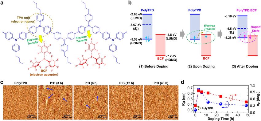
Fig. 1 Doping reaction for SWIR absorption and device structure. a Scheme for the doping reaction between PolyTPD and BCF (see
photographs of solutions according to the doping time on the right top) and illustration of the SWIR-OPTR structure with the BCF-doped
PolyTPD GSL (right bottom). b Optical absorption spectra of the BCF-doped PolyTPD (PolyTPD:BCF = P:B) films coated on quartz substrates
(annealed at 120 °C for 30 min) according to the doping time (inset: corresponding photographs). c Optical density as a function of doping
time at various wavelengths (data taken form b). d Photoelectron (PE) yield spectra for the BCF-doped PolyTPD films annealed at 120 °C for
30 min.
conjugation length is considered to deliver a managed absorption solutions. Upon adding the BCF solution to the PolyTPD solution,
range suitable for SWIR by varying the parameters, such as the solution color was noticeably changed and darkened with
backbone structure of conjugated polymers, types of dopants, time (see Fig. 1a right top and Supplementary Fig. 1). Considering
doping time and temperature, dopant concentration, etc. the change of solution colors with time, the doping reaction might
In this study, we demonstrate that the well-controlled SWIR be very quick and enter a stabilizing stage after 3 h at room
absorption (up to λ = ~3200 nm) can be achieved from a temperature. In addition, no clues on any reverse reaction (de-
polytriarylamine, poly[N,N′-bis(4-butylphenyl)-N,N′-bis(phenyl) doping) could be observed from the solutions reacted up to 48 h.
benzidine] (PolyTPD), by the time-dependent BCF doping at a To further understand, the optical absorption spectra were
fixed BCF concentration. The SWIR absorption intensity of the BCF- measured for the PolyTPD:BCF (P:B) films that were coated from
doped PolyTPD films was gradually increased with the doping corresponding solutions with different doping time. As shown in
time at a fixed BCF concentration of PolyTPD:BCF (P:B = 1:1 by Fig. 1b, the PolyTPD:BCF film from the mixture solution reacted for
weight or molar ratio) and almost saturated at 48 h. The optimized 3 h delivered a new broad optical absorption peak at a
BCF-doped PolyTPD films were applied as a gate-sensing layer wavelength (λ) range between 1000 and >3200 nm. This new
(GSL) in a geometry of organic field-effect transistors (OFETs). The absorption peak was quickly grown up to 10 h and then its
device results showed that the SWIR-OPTRs with the BCF-doped intensity was slowly increased (see Fig. 1c and Supplementary
Fig. 2). Similarly, a new optical absorption peak was also found in
PolyTPD GSLs could successfully detect the SWIR light up to
the visible range between λ = 420 nm and λ = 570 nm, and grown
λ = 3200 nm with high sensing stability and the SWIR sensitivity
with the doping time (refer to the optical absorption spectrum of
could be controlled by adjusting the gate voltage. BCF in Supplementary Fig. 3). A close look into the optical
absorption peaks in the UV–visible range finds that the original
RESULTS absorption peak (between λ = 280 nm and λ = 420 nm) of
PolyTPD was gradually decreased with the doping time (see
Doping reaction leading to strong SWIR absorption
Supplementary Fig. 4). This phenomenon means that the density
The doping reaction between PolyTPD and BCF was first examined of state (ground) in PolyTPD was decreased by the doping
by adding the BCF solution (40 mg ml−1, chlorobenzene (CB)) to reaction leading to the formation of two states: (1)
the PolyTPD solution (40 mg ml−1, CB) at room temperature λ = 420–570 nm and (2) λ = 1000–3200 nm (and higher).
(25 °C). As seen from the chemical structures in Fig. 1a, neither As a consequence, the ionization potential was gradually
PolyTPD nor BCF has a reactive functional group so that no reduced for the PolyTPD:BCF (BCF-doped PolyTPD) films with
chemical reactions involving the formation of covalent bonds and/ the doping time (tD) (Fig. 1d and Supplementary Fig. 5), indicative
or ionic moieties can be expected from the present mixed of the lowering in the highest occupied molecular orbital (HOMO)
npj Flexible Electronics (2021) 10 Published in partnership with Nanjing Tech University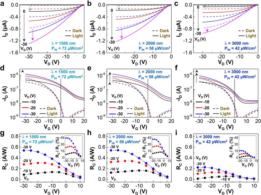
C. Lee et al.
                                                                                                                                                3

Fig. 2 Spectroscopic analysis according to doping time. a FT-IR spectra, b Raman spectra, c ESR spectra, d–f XPS spectra (C1s, F1s, and N1s),
g, h UPS spectra, and i change of the HOMO energy level and work function (WF) for the BCF-doped PolyTPD (P:B) films annealed at 120 °C for
30 min.

energy of PolyTPD by the BCF doping. The resulting PolyTPD:BCF           with the doping time. In other words, the ESR results confirm that
films were employed as a GSL for the SWIR-sensing OPTRs, as               the doping reaction between PolyTPD and BCF is dependent on
illustrated in Fig. 1a (right bottom)24. It is worthy to note that the   the doping time. Next, the core level environment of atoms in the
PolyTPD:BCF layers were well formed and stable without any               PolyTPD:BCF films was investigated with X-ray photoelectron
deformation upon wet coatings of subsequent polymeric layers             spectroscopy (XPS). The intensity of C1s and F1s peaks (in BCF)
because they were insoluble in n-butyl acetate (NBA) solvent used        was gradually increased with the doping time, but the binding
for the poly(methyl methacrylate) (PMMA) layer (see Supplemen-           energy (BE) of these XPS peaks was almost unchanged (Fig. 2d, e).
tary Fig. 6).                                                            The same trend was measured for the N1s peak (in PolyTPD), as
                                                                         can be clearly observed in Fig. 2f. This result reflects that the
Spectroscopic characterizations and doping mechanism                     extent of doping reaction between PolyTPD and BCF was
The atomic and molecular level changes in PolyTPD by the BCF             increased with time, but the core level environment of atoms
doping was investigated by various spectroscopic measurements            was not affected by the doping reaction.
on the PolyTPD:BCF films. The Fourier transform-infrared (FT-IR)             For further understanding, the detailed energy level (band)
spectra confirm the existence of BCF in the PolyTPD:BCF films              change in PolyTPD by the BCF doping was investigated with
because C = C–F (1645 cm−1) and B–C (1015 cm−1) peaks were               ultraviolet photoelectron spectroscopy (UPS). As shown in the UPS
measured together with a broadened C = C shoulder at                     spectra (Fig. 2g), a pronounced spectral shift toward a lower BE
~1510 cm−1 (see Fig. 2a and Supplementary Fig. 7). The peak              direction was measured for the PolyTPD:BCF films compared to
intensity of C–N stretching at 1320 cm−1 was gradually reduced           the pristine PolyTPD film. A close look into the valence band (level)
with the doping time, which can be attributable to the change of         edge region (A in Fig. 2g) finds that the onset BE of PolyTPD was
nitrogen environment by the BCF doping46,47. The existence of            largely shifted from 1.91 to ca. 0.78 eV by the BCF doping (see
BCF can be further evidenced by the doping time-dependent                Fig. 2h). This means that the extraction of electrons became
Raman intensity change for the aromatic peaks at                         relatively easier for the PolyTPD:BCF films than the pristine
~1185–1210 cm−1 (see Fig. 2b and Supplementary Fig. 8). The              PolyTPD film, which is in agreement with the ionization potential
intensity ratio of the CH2 twist peaks at 1290–1315 cm−1 was             change in Fig. 1d. As shown in Fig. 2h, the calculated HOMO
considerably changed by the BCF doping, which can be ascribed            energy level was abruptly shifted from −5.58 eV (pristine PolyTPD
to a large-scale rearrangement of butyl groups in PolyTPD by the         film) to −5.34 eV by the BCF doping for 3 h, and then further to
binding (doping) of BCF molecules to the PolyTPD chains.                 −5.28 eV after 48 h (see Supplementary Fig. 9 for the detailed
   As shown in Fig. 2c, an electron spin resonance (ESR) signal was      calculations). Note that the HOMO energy level of the pristine
measured at ~3355 G for the PolyTPD:BCF films even though no              PolyTPD molecules dissolved in dichloromethane (solvent) was
ESR signal was detected for the pristine PolyTPD film. This result        measured to −5.48 eV with cyclic voltammetry (CV; see Supple-
indicates the generation of unpaired (single) electrons in the           mentary Fig. 10a).
PolyTPD:BCF films. Further investigation finds that the ESR signal            Based on the above characterization results, it is proposed that
became intensified as the doping time increased, which can be             the doping reaction between PolyTPD and BCF occurs via the
directly related to the increased number of unpaired electrons           electron transfer from PolyTPD to BCF on a molecular scale, as

Published in partnership with Nanjing Tech University                                                     npj Flexible Electronics (2021) 10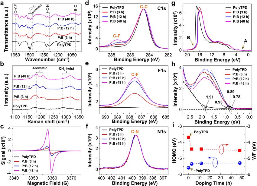
C. Lee et al.
4

    Fig. 3 Change of energy level and morphology. a Illustration for the electron transfer between PolyTPD and BCF. b Flat energy level (band)
    diagrams for the explanation of electron transfer-mediated doping mechanism between PolyTPD and BCF. c Phase-mode AFM images (2 μm ×
    2 μm) for the PolyTPD:BCF films (48 h) according to the doping time. d Change of root-mean-square roughness (Rg) and phase angle (AP)
    according to the doping time for the PolyTPD:BCF films (48 h).

                                                                            illustrated in Fig. 3a. In more detail, the TPA units of PolyTPD act as
                                                                            an electron donor, while the BCF molecules play as an electron-
                                                                            accepting role in the doping reaction. This electron transfer-based
                                                                            doping reaction can be further explained by the three-step
                                                                            process leading to the change of energy level (band), as depicted
                                                                            in Fig. 3b. The electron transfer upon doping reaction in solutions
                                                                            leads to a positive polaron state (radical cation) in PolyTPD, while
                                                                            it bestows a negative state (radical anion) to BCF (see the middle
                                                                            diagram in Fig. 3b). In terms of PolyTPD, the HOMO energy level
                                                                            was increased from −5.58 eV (pristine PolyTPD film) to −5.28 eV
                                                                            (PolyTPD:BCF film), but the LUMO energy level was decreased
                                                                            from −2.68 eV (pristine PolyTPD film) to −3.18 eV (PolyTPD:BCF
                                                                            film) by the BCF doping (all data were taken from the UPS spectra
                                                                            of film samples). Note that the HOMO and LUMO energy levels of
                                                                            BCF molecules (in solution) in Fig. 3b were taken from previous
                                                                            reports (our CV measurement could deliver only the LUMO energy
                                                                            level of −5.01 eV for the BCF solution as given in Supplementary
                                                                            Fig. 10b)48. Here, a coulombic interaction between these counter
                                                                            charges may occur, leading to physically binding the two charged
                                                                            species in the films, so that the BCF-doped PolyTPD components
                                                                            can be kept in the films without removal upon spin-coating
                                                                            processes. Therefore, the BCF-doped PolyTPD complexes have
                                                                            new energy (gap) states with the lowest energy of ca. −5.28 eV
                                                                            that can be corresponded to the optical absorption edge (λ = ca.
                                                                            3200 nm; see Fig. 1b). Considering a possible interaction of BCF
                                                                            molecules to various conformational states of the PolyTPD chains,
                                                                            the BCF-doped PolyTPD complexes are regarded to make a broad
                                                                            range of energy states as measured from the absorption spectra
                                                                            (λ = 420–570 nm and λ = 1000–3200 nm in Fig. 1b). Note that the
                                                                            new optical absorption peaks (λ = 420–570 nm) can be assigned
                                                                            to the optical transition between the HOMO (−5.28 eV) and LUMO
                                                                            (−3.18 eV) energy levels of the BCF-doped PolyTPD complexes,
                                                                            when it comes to the band edge of these peaks (ca. 590 nm,
    Fig. 4 Basic OFET characteristics. a Output and b transfer curves       2.1 eV). Finally, the atomic force microscope (AFM) images
    for the OFETs with the PolyTPD:BCF layers (48 h; inset: photographs     unveiled an uneven morphology featuring a nanodot in the
    for the devices) in the dark. c Change of hole mobility (μh) and        PolyTPD:BCF films, which are varied with the doping time (Fig. 3c
    threshold voltage (VTH) as a function of drain voltage (data were       and Supplementary Fig. 11). The nanodots were relatively more
    taken from the transfer curves in Supplementary Fig. 12).
                                                                            pronounced at 3 h and became gradually degenerated with the
                                                                            doping time, as supported by the root-mean-square roughness
                                                                            (Rg) and phase angle changes in Fig. 3d. It is speculated that the

    npj Flexible Electronics (2021) 10                                                        Published in partnership with Nanjing Tech University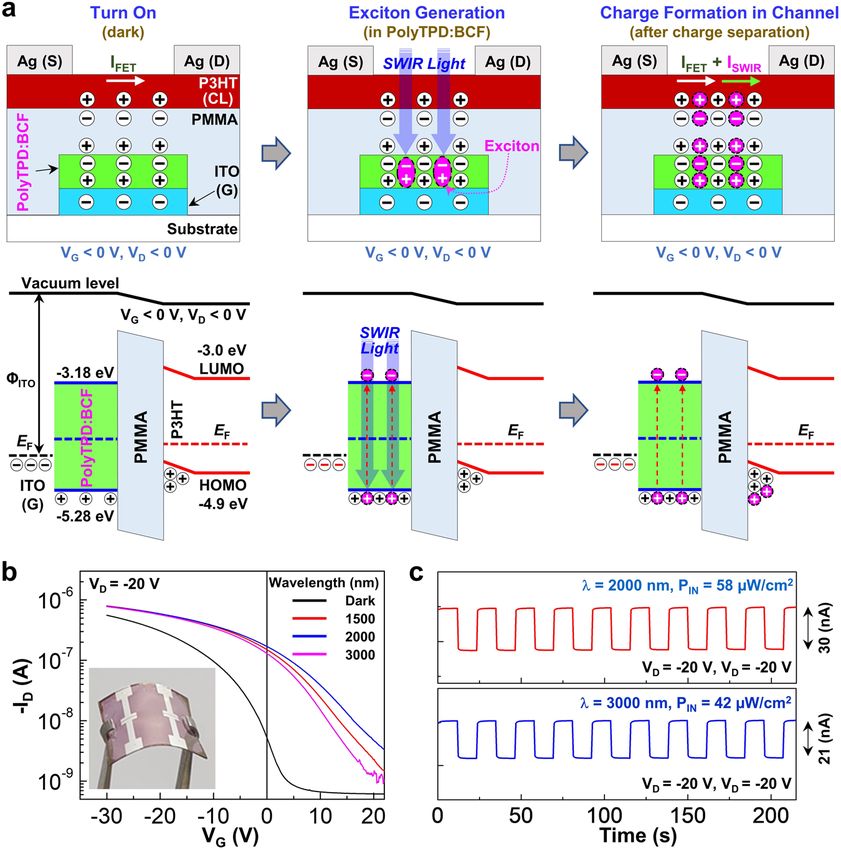
C. Lee et al.
                                                                                                                                             5
nanodots might be formed due to the existence of heterogeneous        λ = 2000 nm, and 0.41 eV at λ = 3000 nm). The ratio (RC/RT) of RC
states that are related to the pristine PolyTPD and BCF-doped         to theoretical maximum photosensitivity (RT), which is irrelevant to
PolyTPD phases.                                                       the kind of materials, reached 45% (λ = 1500 nm), 41% (λ = 2000
                                                                      nm), and 16% (λ = 3000 nm) at VG = VD = −30 V, respectively (see
Transistor performances in the dark                                   inset graphs in Fig. 5g–i).
The OFETs with the BCF-doped PolyTPD layers (48 h) placed
between the indium-tin oxide (ITO) electrodes and the PMMA            Sensing mechanism and flexible SWIR-OPTRs
layers were examined in the dark. As shown in Fig. 4a, the output     On the basis of above results, a possible three-step mechanism
curves deliver a typical behavior of p-channel transistors when it    can be proposed for the operation of the present SWIR-OPTRs
comes to the drain current (ID) change according to the drain         with the PolyTPD:BCF GSLs (see Fig. 6a): (1) the field-effect charges
voltage (VD) at a fixed gate voltage (VG). In addition, the            are generated in each layer by applying the negative drain and
drain current in the output curves became saturated as the drain      gate voltages to the corresponding electrodes. The field-effect
voltage increased, indicative of proper working of field-effect        charges lead to the deformation in the energy levels (bands)
transistors. The transfer curves in Fig. 4b clearly exhibited the     inside devices (see Supplementary Fig. 14). This first step enables
characteristics of p-channel transistors as the drain current was     the SWIR-OPTRs to turn on and ready for operation. (2) When the
pronouncedly increased with the gate voltage. It is noted that a      SWIR light is illuminated to the channel area, it passes through
good linearity was obtained for the ID0.5–VG plot, implying a         the P3HT and PMMA layers without absorption and reaches the
constancy in charge transport with the gate voltage in spite of the   PolyTPD:BCF GSLs. Then the PolyTPD:BCF GSLs absorb the SWIR
presence of the PolyTPD:BCF layers. As shown in Fig. 4c, the hole     light leading to the generation of excitons, which is instant and
mobility (μh) and threshold voltage (VTH) were almost linearly        may not largely change the energy levels when it comes to the
changed with the drain voltage (see all transfer curves in            neutral state of excitons. (3) The excitons generated in the
Supplementary Fig. 12). This result supports the voltage-             PolyTPD:BCF GSLs are subjected to a field-induced charge
dependent stable characteristics of the present OFETs with the        separation process leading to the rearrangement of individual
BCF-doped PolyTPD layers (48 h).                                      charges (holes and electrons). These individual charges act as an
                                                                      additional electric field inside the devices so that more holes can
SWIR light-sensing device characteristics                             be formed in the P3HT channel layers (see the deformed energy
The SWIR light-sensing performance was tested by illuminating         levels due to the photogenerated charge build-up). The resulting
three different monochromatic SWIR light (λ = 1500, 2000, and         photocurrent (ISWIR) is added to the original field-effect current
3000 nm) to the channel area of the OFETs with the PolyTPD:           (IFET), which leads to the increased drain current in the devices
BCF layers (48 h). The incident light intensity (PIN) was adjusted    upon the SWIR illumination.
to 72, 58, and 42 µW cm−2 at λ = 1500, 2000, and 3000 nm,                 For a possible application of the present SWIR-OPTR technology
respectively. As observed from the output curves in Fig. 5a–c,        to flexible electronics, the flexible SWIR-OPTRs with the PolyTPD:
the drain current was certainly increased upon illumination with      BCF GSLs were fabricated using the ITO-coated poly(ethylene
the SWIR light irrespective of the gate voltage. The higher the       naphthalene) (PEN) film substrates. As shown in Fig. 6b, the drain
gate voltage, the higher the drain current in the output curves       current in the transfer curves was noticeably increased upon
for all the three SWIR cases. This result basically indicates that    illumination with the SWIR light (λ = 1500, 2000, and 3000 nm; see
the PolyTPD:BCF layers (48 h) work properly as a GSL for the          the dark characteristics in Supplementary Fig. 15). It is worthy to
SWIR light up to λ = 3000 nm, achieving a SWIR-OPTR. As shown         note that the threshold voltage in the transfer curves was
in Fig. 5d–f, the drain current in the transfer curves was            pronouncedly shifted by the SWIR illumination, which is in
noticeably increased by the SWIR illumination over the whole          accordance with the phenomena in the case of using the glass
gate voltage. A particular attention is paid to the SWIR-driven       substrates (see Fig. 5). As shown in Fig. 6c, the present flexible
huge jump in drain current at around turn-on voltage region,          SWIR-OPTRs exhibited a good sensing stability upon on/off
which could lead to the shift of threshold voltage toward a           modulations of the incident SWIR light (PIN = 58 µW cm−2 at
lower gate voltage direction (in an absolute value). Note that        λ = 2000 nm and 42 µW cm−2 at λ = 3000 nm). In order to
almost no meaningful change of drain current and threshold            examine the durability of the flexible SWIR-OPTRs, the device
voltage was measured for the OFETs with the pristine PolyTPD          performances in the dark were measured before and after
layer (in the GSL position) under illumination with the three         bending at a radius of curvature of 7.5 mm. The result showed
different SWIR light (see Supplementary Fig. 13).                     that the output and transfer curves were almost similar (very small
   To investigate the detailed performances of the present SWIR-      change) even after bending (see Supplementary Fig. 16). In
OPTRs, the photoresponsivity (RC), representing the ratio of net      particular, the bended flexible SWIR-OPTRs (bended state at a
photocurrent to incident light intensity after removing the dark      radius of curvature of 7.5 mm) exhibited noticeable drain current
drain current, was extracted from the transfer curves (see            increase and threshold voltage shift upon illumination with the
Fig. 5g–i). As the gate voltage increased (negatively), the           three different SWIR light (see Supplementary Fig. 17). In addition,
photoresponsivity was initially increased and levelled off at         the drain current from the bended flexible SWIR-OPTRs was
the highest drain voltage (VD = −30 V). However, irrespective of      gradually increased with the applied gate and/or drain voltages.
the SWIR wavelength, the photoresponsivity was decreased again        This result reflects that the PolyTPD:BCF layers play a durable GSL
after reaching a maximum at the lower drain voltages. The initial     in the sensing of SWIR light even in the geometry of flexible
rise in RC can be assigned to the increased collection efficiency of   substrates.
photogenerated charges with the gate voltage, whereas the
saturating and/or decreasing RC afterward can be attributed to the
narrowing of neutral zones for photoexcitation in the GSLs, owing     DISCUSSION
to the overwhelming of field-effect zones49,50. Because this           The present breakthrough work showed that a triarylamine-based
phenomenon was similarly measured for the three different SWIR,       polymer (PolyTPD) could be successfully doped with a fluorinated
the present SWIR-OPTRs with the PolyTPD:BCF GSLs are con-             small molecule with high electron affinity (BCF), and the resulting
sidered to work with the same mechanism of photoexcitation and        doped polymer (BCF-doped PolyTPD) films were able to act as an
charge generation/separation in spite of a large energy gap in the    efficient GSL for SWIR-OPTRs. The BCF-doped PolyTPD was found
incident SWIR light (0.83 eV at λ = 1500 nm, 0.62 eV at               to have a newly evolved optical absorption peak, covering a broad

Published in partnership with Nanjing Tech University                                                  npj Flexible Electronics (2021) 10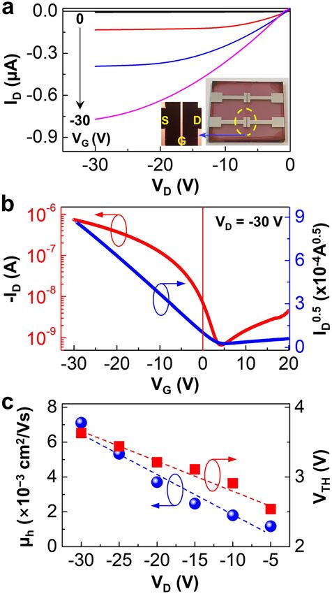
C. Lee et al.
6

    Fig. 5 Device characteristics under SWIR illumination. a–c Output and d–f transfer curves for the SWIR-OPTRs with the PolyTPD:BCF GSLs
    (48 h) upon illumination with three different SWIR light (λ = 1500, 2000, and 3000 nm). Note that VG and VD were negatively increased by
    −10 V in the output and transfer curves, respectively. g–i Photoresponsivity (RC) as a function of VG at three different drain voltages under
    illumination with the SWIR light (λ = 1500, 2000, and 3000 nm; inset: the ratio of the measured photoresponsivity to the theoretical maximum
    photoresponsivity (RT) at a given wavelength). Note that all RC values were obtained after removing the dark current from the transfer curves
    in d, e, and f.

    range of NIR and SWIR between 1000 and >3200 nm, which was               METHODS
    gradually increased upon doping reaction up to 48 h at room              Materials and solutions
    temperature. The in-depth spectroscopic analysis unveiled that           PolyTPD (average molecular weight = 24 kDa) and BCF (formula weight =
    the doping reaction between PolyTPD and BCF occurs by the                511.98) were purchased from Lumtec (Hsin-Chu, Taiwan) and Sigma
    ground-state electron transfer from PolyTPD to BCF on a                  Aldrich Co. (St Louis, Mo, USA), respectively. P3HT (weight-average
    molecular scale. The single (unpaired) electrons remained in             molecular weight = 70 kDa, polydispersity index = 1.7, regioregularity
    PolyTPD after doping were clearly measured by the ESR                    >97%) and PMMA (weight-average molecular weight = 120 kDa, poly-
    measurement, while the HOMO energy level shift in the BCF-               dispersity index = 2.2) were received from Rieke Metals (Lincoln, NE, USA)
    doped PolyTPD film was confirmed by the photoelectron                      and Sigma Aldrich (St Louis, Mo, USA), respectively. The P3HT solutions
                                                                             were prepared using toluene (Sigma Aldrich) at a solid concentration of
    spectroscopy measurements. The AFM examination revealed the
                                                                             12.5 mg ml−1, while NBA (Sigma Aldrich) was used as a solvent for the
    presence of heterogeneous states during doping, which might be           preparation of the PMMA solutions (concentration = 80 mg ml−1). All
    originated by the co-existence of two different phases (the pristine     solutions were continuously stirred at 60 °C for 24 h before spin-coating.
    PolyTPD and BCF-doped PolyTPD domains). The OFETs with the
    BCF-doped PolyTPD layers delivered typical p-channel transistor
                                                                             Doping reaction and film preparation
    characteristics in the dark. Upon illumination with the SWIR light
                                                                             To dope PolyTPD with BCF, the binary solutions of PolyTPD (P) and BCF (B)
    (1500, 2000, and 3000 nm), the BCF-doped PolyTPD layers could
                                                                             (P:B = 1:1 by weight) were prepared at a solid concentration of 40 mg ml−1
    act as an efficient SWIR-detecting GSL in the SWIR-OPTRs. The RC          using CB as a solvent. These solutions were subjected to continuous
    of the SWIR-OPTRs with the BCF-doped PolyTPD GSLs reached                stirring on a hot plate stirrer at a fixed temperature of 25 °C by varying the
    ~538 mA W−1 (λ = 1500 nm), ~541 mA W−1 (λ = 2000 nm), and                doping time up to 168 h. These solutions were carefully monitored and
    ~222 mA W−1 (λ = 3000 nm), which correspond to 45, 41, and 16%           one solution per every 1 h was taken for spin-coating, in order to examine
    of the theoretical responsivity at each wavelength. Further              the change in color and optical absorption spectrum. The BCF-doped
    improvement in photoresponsivity can be achievable by optimiz-           PolyTPD films (thickness = 60 nm) were spin-coated on quartz substrates
    ing the thickness of BCF-doped PolyTPD layers, doping concen-            and thermally treated at 120 °C for 30 min for the optical measurements.
    trations, multilayer structures, etc. Finally, the flexible SWIR-OPTRs    For the spectroscopic and morphological measurements (FT-IR, XPS, PEYS,
                                                                             UPS, AFM, and scanning electron microscope (SEM)), the same spin-
    showed stable sensing characteristics upon on/off modulations of
                                                                             coating processes were applied to prepare the BCF-doped PolyTPD films
    the incident SWIR light. Hence, the present pioneering work is           on the ITO-coated glass substrates, in order to secure the same condition
    expected to be a stepping stone toward a wide-spreading of the           as for the device fabrication. However, for the ESR spectroscopy
    ground-state doping research of nitrogen-containing polymers             measurement, the BCF-doped PolyTPD films were prepared on a PEN
    and their applications for efficient SWIR-sensing photodetectors          substrate (width: 3 mm, length: 20 mm) in order to get unperturbed
    required for next-generation soft/flexible electronics.                   electron spin signals.

    npj Flexible Electronics (2021) 10                                                           Published in partnership with Nanjing Tech University
C. Lee et al.
7
Fig. 6 Working mechanism and flexible SWIR-OPTRs. a Proposed mechanism for the operation of the SWIR-OPTRs with the PolyTPD:BCF
GSLs under the SWIR illumination (top: device structures, bottom: energy level diagrams): (left) turned-on state in the dark; (middle) exciton
generation in the PolyTPD:BCF GSLs upon illumination with the SWIR light; (right) charge separation from photogenerated excitons and
formation of induced charges in the channel layer. ΦITO, IFET, ISWIR, and EF stand for the work function of ITO gate electrode, the drain current
by field-effect phenomenon, the drain current by SWIR illumination, and Fermi energy level, respectively. b Transfer curves (VD = −20 V) for
the flexible SWIR-OPTRs with the PolyTPD:BCF GSLs (48 h) under illumination with the SWIR light (λ = 1500, 2000, and 3000 nm). c Change of
photocurrent upon optical modulations of the incident SWIR light (λ = 2000 and 3000 nm) for the flexible SWIR-OPTRs.
Device fabrication films were measured using a UV/Vis/NIR spectrometer (Lambda 750,
To fabricate SWIR-OPTRs, the ITO-coated glass substrates (sheet resistance PerkinElmer, Houston, TX, USA). A FT-IR spectrometer (5700 Continum,
= 10 Ω cm−2) were underwent via a photolithography process for the Thermo Scientific, Inc.) was used to characterize specific functional groups in
patterning of the ITO stripe (1 mm × 12 mm) used as a gate (G) electrode. the film samples in an attenuated total reflection mode. The Raman spectra
The patterned ITO–glass substrates were subjected to wet-clean processes of films were measured using a Raman spectrometer (Almega X, Thermo
using acetone and isopropyl alcohol (30 min), followed by dry cleaning Scientific, Inc.) at an excitation wavelength of 532 nm. The core level atom
steps using a UV-ozone cleaner (28 mW cm−2 for 20 min, Ahtech, Korea). enivronments in the films were characterized by employing an XPS
The BCF-doped PolyTPD layers (thickness = 60 nm) were deposited on the spectrometer (ESCALAB 250, Thermo Scientific, Inc.). The HOMO energy level
patterned ITO–glass substrates by spin-coating at 2000 r.p.m. for 60 s. The change of the BCF-doped PolyTPD films were measured and characterized
side parts of the coated BCF-doped PolyTPD layers were removed using CB using a UPS spectrometer (Nexsa-XPS system, Thermo Scientific, Inc.). The
to achieve the final BCF-doped PolyTPD stripes (1.1 mm × 12 mm), ionization potentials of films were measured using a PE yield spectrometer
followed by thermal treatment at 120 °C for 30 min. Next, the PMMA (PEYS, AC-2, Rieken-Keikki, Japan). The CV measurements were performed
gate-insulating layers (thickness = 450 nm) were spin-coated on the for the pristine solutions of PolyTPD and BCF (solvent: dichloromethane)
patterned BCF-doped PolyTPD layers at 2000 r.p.m. for 60 s and thermally using an electrochemical measurement system equipped with a potentio-
treated at 120 °C for 30 min. Finally, the P3HT channel layers (thickness = stat/impedance analyzer (Versastat 4, Ametek, Inc.; see further details in
60 nm) were spin-coated on the PMMA layers at 1500 r.p.m. for 30 s and Fig. S10). The existence of radicals (unpaired electrons) in films was
soft-baked at 70 °C for 15 min. These polymer multilayer samples were investigated by employing an ESR spectrometer (EMXplus-9.5/2.7, Bruker,
transferred to a vacuum chamber installed inside a nitrogen-filled USA). The surface morphology of film samples was measured using an AFM
glovebox system. When the base pressure reached ca. 1 × 10⁻⁶ torr, silver (Nanoscope IVa, Digital Instruments, Tonawanda, NY, USA), while the film
(Ag) metals were thermally evaporated on the P3HT layers through a surface and cross-section parts of SWIR-OPTRs were measured using a high-
shadow mask to make the 60-nm-thick source (S) and drain (D) electrodes. resolution SEM (SU-8230, Hitachi, Japan). The characteristics (output and
The channel length and width of the SWIR-OPTRs were 70 µm and 2 mm, transfer curves) of OFET devices were measured using a semiconductor
respectively. All devices and film samples were wrapped and safely stored parameter analyzer (4200 SCS, 2636B, Keithley, USA). In order to test the
inside the argon-filled glovebox until measurements. performances of SWIR-OPTRs, the channel area of transistors was
illuminated with a monochromatic SWIR light from a monochromator
(DK240, Spectral Products, Albuquerque, NM, USA) that spectrally filters the
Measurement and characterizations source IR beam generated from an IR emitter system (11 W, ASB-IR-12K,
The thickness of films was measured using a nanoscale surface profiler Spectral Products). The incident light intensity (PIN) of each monochromatic
(DektakXT, Bruker, USA). The optical absorption spectra of solutions and SWIR light was controlled by employing neutral density filter sets, while the
Published in partnership with Nanjing Tech University npj Flexible Electronics (2021) 10C. Lee et al.
8
SWIR light power was exactly measured using an optical power meter 19. Arquer, F. P. G., Armin, A., Meredith, P. & Sargent, E. H. Solution-processed
(PM100D, Thorlabs, Newton, NJ, USA). Two different approaches for the semiconductors for next-generation photodetectors. Nat. Rev. Mater. 2, 1–17
calculation of device current density (JD) were applied: (1) JD,IP = ID/(L × W) in (2017).
a viewpoint of in-plane (IP) direction (actual current flow direction); (2) JD, 20. Liang, F. X., Wang, J. Z., Li, Z. P. & Luo, L. B. Near‐infrared‐light photodetectors
OOP = ID/(T × W) in a viewpoint of out-of-plane (OOP) direction (SWIR light based on one‐dimensional inorganic semiconductor nanostructures. Adv. Opt.
illumination direction), where T, W, and L stand for the channel thickness, Mater. 5, 1700081 (2017).
width, and length, respectively. The PIN value (power density) of SWIR light 21. Lou, Z. & Shen, G. Flexible photodetectors based on 1D inorganic nanostructures.
was calculated with PIN = P/(L × W), where P is the incident light power (in a Adv. Sci. 3, 1500287 (2016).
unit of W). The RC values from JD,IP were used in Fig. 5 (note that the same 22. Teng, F., Hu, K., Ouyang, W. & Fang, X. Photoelectric detectors based on inorganic
trend in RC was obtained for JD,OOP). p‐type semiconductor materials. Adv. Mater. 30, 1706262 (2018).
Methods and any associated references are available in the online 23. Zhao, H. et al. Self-driven visible-near infrared photodetector with vertical
version of the paper. CsPbBr3/PbS quantum dots heterojunction structure. Nanotechnology 31, 035202
(2019).
24. Han, H., Lee, C., Kim, H. & Kim, Y. Flexible near-infrared plastic phototransistors
DATA AVAILABILITY with conjugated polymer gate-sensing layers. Adv. Funct. Mater. 28, 1800704
The data that support the findings of this study are available from the corresponding (2018).
author upon reasonable request. 25. Lee, C. et al. Organic phototransistors with chemically doped conjugated polymer
interlayers for visible and near infrared light detection. IEEE J. Sel. Top. Quant. 24,
1–7 (2018).
Received: 4 November 2020; Accepted: 16 February 2021; 26. Kim, H., Wu, Z., Eedugurala, N., Azoulay, J. D. & Ng, T. N. Solution-processed
phototransistors combining organic absorber and charge transporting oxide for
visible to infrared light detection. ACS Appl. Mater. Interfaces 11, 36880–36885
(2019).
27. Li, N., Lan, Z., Cai, L. & Zhu, F. Advances in solution-processable near-infrared
REFERENCES phototransistors. J. Mater. Chem. C 7, 3711–3729 (2019).
1. Mueller, T., Xia, F. & Avouris, P. Graphene photodetectors for high-speed optical 28. Suk, J. W. et al. Enhancement of the electrical properties of graphene grown by
communications. Nat. Photonics 4, 297–301 (2010). chemical vapor deposition via controlling the effects of polymer residue. Nano
2. Luke, T. D. W. et al. Metabolic profiling of early-lactation dairy cows using milk Lett. 13, 1462–1467 (2013).
mid-infrared spectra. J. Dairy Sci. 102, 1747–1760 (2019). 29. Boonlakhorn, J., Putasaeng, B., Kidkhunthod, P. & Thongbai, P. Improved dielectric
3. Simone, G. et al. Near-infrared tandem organic photodiodes for future application properties of (Y+Mg) co-doped CaCu3Ti4O12 ceramics by controlling geometric
in artificial retinal implants. Adv. Mater. 30, 1804678 (2018). and intrinsic properties of grain boundaries. Mater. Des. 92, 494–498 (2016).
4. Villaseñor-Aguilar, M. J. et al. A maturity estimation of bell pepper (capsicum 30. London, A. E. et al. Donor–acceptor polymers with tunable infrared photo-
annuum l.) by artificial vision system for quality control. Appl. Sci. 10, 5097 (2020). response. Polym. Chem. 8, 2922–2930 (2017).
5. Yang, M. et al. Ultrahigh stability 3D Ti Bi2Se3/MoO3 thin film heterojunction 31. Han, J. et al. Low-bandgap donor–acceptor polymers for photodetectors with
infrared photodetector at optical communication waveband. Adv. Funct. Mater. photoresponsivity from 300 nm to 1600 nm. J. Mater. Chem. C 5, 159–165 (2017).
30, 1909659 (2020). 32. Li, M. et al. Phenanthrene condensed thiadiazoloquinoxaline donor-acceptor
6. Thomas, L., Sorathiya, V., Patel, S. K. & Guo, T. Graphene‐based tunable near‐ polymer for phototransistor applications. Chem. Mater. 27, 2218–2223 (2015).
infrared absorber. Micro. Opt. Technol. Lett. 61, 1161–1165 (2019). 33. Shi, H. et al. Effective approaches to improve the electrical conductivity of PEDOT:
7. Saritha Devi, H. N. V., Swapna, M. N. S. & Sankararaman, S. I. Cost-effective green PSS: a review. Adv. Electron. Mater. 1, 1500017 (2015).
synthesis of boron-rich carbide coatings for infrared windows and night-vision 34. Cho, S., Lee, J. S. & Joo, H. Recent developments of the solution-processable and
optics. Phys. Status Solidi A 217, 1901014 (2020). highly conductive polyaniline composites for optical and electrochemical appli-
8. Wu, Z., Yao, W., London, A. E., Azoulay, J. D. & Ng, T. N. Elucidating the detectivity cations. Polymers 11, 1965 (2019).
limits in shortwave infrared organic photodiodes. Adv. Funct. Mater. 28, 1800391 35. Massonnet, N., Carella, A., de Geyer, A., Faure-Vincent, J. & Simonato, J. P. Metallic
(2018). behaviour of acid doped highly conductive polymers. Chem. Sci. 6, 412–417
9. Wu, Z. et al. The role of dielectric screening in organic shortwave infrared pho- (2015).
todiodes for spectroscopic image sensing. Adv. Funct. Mater. 28, 1805738 (2018). 36. Nizioł, J., Gondek, E. & Plucinski, K. J. Characterization of solution and solid state
10. Lin, J. et al. Novel near-infrared II aggregation-induced emission dots for in vivo properties of polyaniline processed from trifluoroacetic acid. J. Mater. Sci. Mater.
bioimaging. Chem. Sci. 10, 1219–1226 (2019). Electron. 23, 2194–2201 (2012).
11. Bhowmik, M. K. et al. Thermal infrared face recognition-a biometric identification 37. Enengl, C. et al. Doping‐induced absorption bands in p3ht:polarons and bipo-
technique for robust security system. In Reviews, Refinements and NewIdeas in larons. Chemphyschem 17, 3836–3844 (2016).
Face Recognition, Vol. 7 (ed. Corcoran, P. M.) 113–120 (IntechOpen, 2011). 38. Jin, Y., Ye, F., Zeigler, M., Wu, C. & Chiu, D. T. Near-infrared fluorescent dye-doped
12. Cao, G. et al. Performance of extended wavelength InGaAs/InAsP SWIR detector. semiconducting polymer dots. ACS Nano 5, 1468–1475 (2011).
In Proc. 7th International Symposium on Advanced Optical Manufacturingand 39. An, Q. et al. Improved efficiency of bulk heterojunction polymer solar cells by
Testing Technologies: Optoelectronics Materials and Devices for Sensing and doping low-bandgap small molecules. ACS Appl. Mater. Interfaces 6, 6537–6544
Imaging. Vol. 9284 (ed. Jiang Y. & Yu, J.) 928406 (SPIE, 2014). (2014).
13. Davis, M. & Greiner, M. E. Indium antimonide large-format detector arrays. Opt. 40. Zhao, X., He, S. & Tan, M. C. Design of infrared-emitting rare earth doped nano-
Eng. 50, 061016 (2011). particles and nanostructured composites. J. Mater. Chem. C 4, 8349–8372 (2016).
14. Akhavan, N. D., Jolley, G., Umana-Membreno, G. A., Antoszewski, J. & Faraone, L. 41. Mansour, A. E. et al. The optical signatures of molecular-doping induced polarons
Design of band engineered HgCdTe nBn detectors for MWIR and LWIR applica- in poly (3-hexylthiophene-2, 5-diyl): individual polymer chains versus aggregates.
tions. IEEE Trans. Electron Devices 62, 722–728 (2015). J. Mater. Chem. C 8, 2870–2879 (2020).
15. Lucey, P. G., Wood, M., Crites, S. T. & Akagi, J. A LWIR hyperspectral imager using a 42. Pingel, P. et al. P-type doping of poly (3-hexylthiophene) with the strong lewis
Sagnac interferometer and cooled HgCdTe detector array. In Proc. Algorithms and acid tris (pentafluorophenyl) borane. Adv. Electron. Mater. 2, 1600204 (2016).
Technologies for Multispectral, Hyperspectral, and Ultraspectral Imagery XVIII. Vol. 43. Ren, X. et al. Organic field-effect transistor for energy-related applications: low-
8390 (eds Shen, S. S. & Lewis P. E.) 83900 (SPIE, 2012). power-consumption devices, near-infrared phototransistors, and organic ther-
16. Hansen, M. P., & Malchow, D. S. Overview of SWIR detectors, cameras, and moelectric devices. Adv. Energy Mater. 8, 1801003 (2018).
applications. In Proc. Thermosense XXX. Vol 6939 (eds Vavilov, V. P. & Burleigh, D. 44. Randell, N. M., Boutin, P. C. & Kelly, T. L. Bisisoindigo: using a ring-fusion approach
D) 69390I (SPIE, 2008). to extend the conjugation length of isoindigo. J. Mater. Chem. A 4, 6940–6945
17. Ouyang, W., Teng, F., He, J. H. & Fang, X. Enhancing the photoelectric perfor- (2016).
mance of photodetectors based on metal oxide semiconductors by charge‐car- 45. Jiang, Y. et al. Fused isoindigo ribbons with absorption bands reaching near-
rier engineering. Adv. Funct. Mater. 29, 1807672 (2019). infrared. Angew. Chem. 130, 10440–10444 (2018).
18. Ni, Z. et al. Plasmonic silicon quantum dots enabled high-sensitivity ultrabroad- 46. Ye, T., Wang, J., Chen, W., Yang, Y. & He, D. Improved performance and repro-
band photodetection of graphene-based hybrid phototransistors. ACS Nano 11, ducibility of perovskite solar cells by well-soluble tris(pentafluorophenyl) borane
9854–9862 (2017). as a p-type dopant. ACS Appl. Mater. Interfaces 9, 17923–17931 (2017).
npj Flexible Electronics (2021) 10 Published in partnership with Nanjing Tech UniversityC. Lee et al.
9
47. Welch, G. C. & Bazan, G. C. Lewis acid adducts of narrow band gap conjugated ADDITIONAL INFORMATION
polymers. J. Am. Chem. Soc. 133, 4632–4644 (2011). Supplementary information The online version contains supplementary material
48. Ye, T., Wang, J., Chen, W., Yang, Y. & He, D. Improved performance and repro- available at https://doi.org/10.1038/s41528-021-00105-z.
ducibility of perovskite solar cells by well-soluble tris (pentafluorophenyl) borane
as a p-type dopant. ACS Appl. Mater. Interfaces 9, 17923–17931 (2017). Correspondence and requests for materials should be addressed to Y.K.
49. Hwang, H. et al. Organic phototransistors with nanoscale phase-separated
polymer/polymer bulk heterojunction layers. Nanoscale 3, 2275–2279 (2011). Reprints and permission information is available at http://www.nature.com/
50. Nam, S. et al. Efficient deep red light-sensing all-polymer phototransistors with reprints
p-type/n-type conjugated polymer bulk heterojunction layers. ACS Appl. Mater.
Interfaces 9, 14983–14989 (2017). Publisher’s note Springer Nature remains neutral with regard to jurisdictional claims
in published maps and institutional affiliations.
ACKNOWLEDGEMENTS
This work was financially supported by the National Research Foundation (NRF) of
Korea (NRF_2018R1D1A3B07046214, NRF_2018R1D1A1B07051075, Basic Science
Research Program_2018R1A6A1A03024962) and the International Cooperative R&D Open Access This article is licensed under a Creative Commons
program funded by the Ministry of Trade, Industry and Energy (MOTIE) and Korea Attribution 4.0 International License, which permits use, sharing,
Institute for Advancement of Technology (KIAT, Project No. P0011262). adaptation, distribution and reproduction in any medium or format, as long as you give
appropriate credit to the original author(s) and the source, provide a link to the Creative
Commons license, and indicate if changes were made. The images or other third party
AUTHOR CONTRIBUTIONS material in this article are included in the article’s Creative Commons license, unless
indicated otherwise in a credit line to the material. If material is not included in the
Y.K. designed this work and C.L. carried out all experiments, including device
article’s Creative Commons license and your intended use is not permitted by statutory
fabrication and measurements. H.K. involved in the analysis of spectroscopy data. C.L.
regulation or exceeds the permitted use, you will need to obtain permission directly
and Y.K. wrote this manuscript.
from the copyright holder. To view a copy of this license, visit http://creativecommons.
org/licenses/by/4.0/.
COMPETING INTERESTS
The authors declare no competing interests. © The Author(s) 2021
Published in partnership with Nanjing Tech University npj Flexible Electronics (2021) 10You can also read