Silicate bonding of sapphire to SESAMs: adjustable thermal lensing for high-power lasers
←
→
Page content transcription
If your browser does not render page correctly, please read the page content below
Research Article                                       Vol. 29, No. 12 / 7 June 2021 / Optics Express 18059

Silicate bonding of sapphire to SESAMs:
adjustable thermal lensing for high-power lasers
L. L ANG , 1,3,* F. S ALTARELLI , 1,3 G. L ACAILLE , 2 S. R OWAN , 2 J.
H OUGH , 2 I. J. G RAUMANN , 1 C. R. P HILLIPS , 1 AND U.
K ELLER 1
1 Institute
          for Quantum Electronics, ETH Zurich, 8093 Zurich, Switzerland
2 Institute
          for Gravitational Research, University of Glasgow, G12 8QQ Glasgow, UK
3 These authors contributed equally to this work
* langl@phys.ethz.ch

Abstract: Silicate bonding is a flexible bonding method that enables room-temperature bonding
of many types of materials with only moderate flatness constraints. It is a promising approach for
bonding components in high power laser systems, since it results in a thin and low-absorption
interface layer between the bonded materials. Here we demonstrate for the first time silicate
bonding of a sapphire window to a SEmiconductor Saturable Absorber Mirror (SESAM) and
use the composite structure to mode-lock a high-power thin-disk laser. We characterize the
fabricated devices both theoretically and experimentally and show how the thermally induced
lens of the composite structure can be tuned both in magnitude and sign via the thickness of
the sapphire window. We demonstrate mode-locking of a high-power thin-disk laser oscillator
with these devices. The altered thermal lens allows us to increase the output power to 233 W, a
70-W-improvement compared to the results achieved with a state-of-the-art SESAM in the same
cavity.

Published by The Optical Society under the terms of the Creative Commons Attribution 4.0 License. Further
distribution of this work must maintain attribution to the author(s) and the published article’s title, journal
citation, and DOI.

1.    Introduction
High-power ultrafast laser sources find many applications in research and industry. The high
peak powers are useful for industrial micro-machining or generation of extreme-ultra-violet and
terahertz radiation, and the ultrashort pulses enable time resolution down to the femtosecond
timescale. Currently, the leading technologies for high power ultrafast lasers use Yb-doped gain
media based on thin-disk, innoslab and fiber configurations [1–4]. All three configurations are
routinely used to generate multi-100-W average output powers, owing to the excellent thermal
characteristics and geometry of the gain material. In a thin-disk laser (TDL), the gain is disk-
shaped with order 100-µm thickness and is used in reflection, with the back-side being attached
to a water-cooled heat-sink. This enables a quasi-one-dimensional heat-flow which results in
highly efficient heat extraction. Consequently, the TDL technology enables the generation of
a high-power laser output directly from an oscillator [1]. Such oscillators are very attractive
due to their lower complexity compared with laser amplifier systems. Ultrafast operation in
TDLs is typically achieved using either SEmiconductor Saturable Absorber Mirror (SESAM)
mode-locking [5] or Kerr-Lens Mode-locking (KLM), which have achieved 350 W [1] and 270
W [6] average output powers, respectively.
   Managing the thermal load on the intracavity components is one of the major challenges in
power-scaling these lasers [7]. Heating of components typically leads to thermal lensing effects,
changing the cavity mode and ultimately limiting performance. In particular, the absorptive
nature of the SESAM leads to a non-negligible heat load and thermal lens on the structure. One

#427192                                                                      https://doi.org/10.1364/OE.427192
Journal © 2021         Received 9 Apr 2021; revised 14 May 2021; accepted 17 May 2021; published 25 May 2021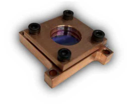
Research Article                                  Vol. 29, No. 12 / 7 June 2021 / Optics Express 18060

possible solution to mitigate this effect is the use of adaptive optics like deformable mirrors to
compensate for the thermal lensing of the intracavity components [8]. While this solution enabled
more than 1 kW of continuous-wave (cw) output power in a TDL, it increases the complexity of
the laser system and has not yet been demonstrated in a high-power mode-locked laser. Many
strategies to more directly combat SESAM thermal lensing have also been explored, such as
thinner substrates, improved contacting [1], or substrate transfer followed by etching [9]. The
substrate transfer technique led to exceptionally flat surfaces (ROC > 1 km) and outstanding heat
extraction. However, due to growth related defects and asymmetries in our MBE machine, we
were not able to obtain a large area sample with such bonding, which would be needed for a
high-power TDL. As an alternative without the inherent thermal lens of the SESAM, nonlinear
mirror mode-locking has also been employed to mode-lock thin-disk lasers [10,11]. So far,
however, mode-locking instabilities prevented the use of this technique above 100-W average
power.
   Here we demonstrate a new approach based on silicate bonding a sapphire window to the
front-face of a SESAM. This bonding process was developed for research in astronomy and
gravitational wave detection [12], and has since been applied to various materials including
sapphire [13]. The optical properties of the bond have recently gathered increasing interest to
expand the range of applications to the field of photonics [14]. In fact, silicate bonding has
a unique combination of properties that make it a promising candidate for the fabrication of
devices for high-power or ultrafast lasers: First, the bond is optically clear and has a high damage
threshold. The bond can therefore be used for intra-cavity bonds in high-power lasers, as we
demonstrate here. Second, the bonding process does not require atomically flat surfaces. In fact,
we apply it successfully to bond standard optical quality sapphire windows to as-grown SESAMs
that show strain induced defects and bending. And third, the bonding process works at room
temperature. This property makes it compatible with devices such as SESAMs whose properties
change when annealed at high temperatures.
   In this work, we demonstrate silicate bonding of sapphire to a SESAM for the first time, to the
best of our knowledge. The fabricated device is used in a high-power TDL, leading to a significant
increase in output power. In a first step, we bond sapphire windows of several thicknesses to
SESAMs. We then characterize the thermal lens of the fabricated devices and implement a 3D
thermo-optic simulation to model the expected behavior. The model shows how the sign and
magnitude of the SESAM thermal lens can be tuned by varying the thickness of the sapphire. We
find good agreement between the experimental results and theoretical predictions. Finally, we
use the new SESAMs to mode-lock a high-power 1030-nm TDL and achieve 233-W average
power, 734-fs pulse duration at 10.2-MHz repetition rate. In the same cavity, we also tested
a conventional high-power SESAM of the type used in our recent high-power results [1], and
obtained up to 160 W mode-locked power. Hence, the sapphire-bonded SESAM enabled a 70-W
improvement in this case. We show how this improvement can be attributed to a change in sign
of the thermal lens of the SESAM.
   Our solution enables high-power compatible mirrors with adjustable thermal properties
fabricated by a versatile and convenient room-temperature bonding technique. In addition
to the SESAM devices we demonstrate in this work, our approach is applicable to a wide
range of reflective optics, including for example vertical external cavity surface emitting lasers
(VECSELs).

2.   Silicate bonding
Silicate bonding uses a hydroxide solution to catalyze the formation of a silica-based network
between two surfaces, effectively bonding them together. The technique was initially developed
for structural applications in instruments for astronomy and became one of the main contributors
to the multiple breakthroughs in gravitational wave detections in the past few years [12,15,16].
Research Article                                Vol. 29, No. 12 / 7 June 2021 / Optics Express 18061

Although not as impactful in photonics, its set of properties have pulled interest from the field
and works on characterization of the optical performances of the bond were carried out [17,18].
It provides advantageous features when compared to the main techniques used in the industry,
adhesive bonding and direct bonding. Other room temperature processes that have been developed
for photonics applications by industrial concerns include Adhesive-Free Bonding (AFB) or
Chemically Activated Direct Bonding (CADB) [19,20].
   Adhesive bonds can display a large range of properties due to the flexibility in formulation.
The main drawbacks come from their organic nature which make them subject to outgassing and
light-induced damage at high power [21,22]. Additionally, there is a large discrepancy between
the thermo-mechanical properties of non-specialized optical adhesives and the substrates they are
used for. This can lead to reduced mechanical stability and increased thermally induced stress
when the component is subject to a change in temperature [21].
   Direct bonding, at low or elevated temperature, constitutes the state-of-the-art of high-
performance bonds for optical applications [23,24]. After a surface activation process, two
components with smooth, matching surfaces (or the capacity to deform sufficiently for them
to match) are able to bond readily at room temperature with moderate pressure. The interface
being free from a third layer, an “ideal” bond is formed with regards to mechanical stability
and outgassing. In practice, it is hard to obtain a homogeneous interface due to the stringent
requirements on the surface quality. Post processing of the component, e.g. heating at high
temperature [23] or applying a voltage across the interface [25], is common to increase the
strength of the bond, but cannot be applied to SESAMs as this would cause changes in their
saturation properties or even destroy them.
   Silicate bonding avoids the issues met with adhesive bonding by only using inorganic
components and forming a thin, glass-like bond which guarantees good mechanical stability
and structural integrity for a wide range of temperatures [26,27]. Compared to direct bonding
techniques, silicate bonding gives some leniency on the surface quality requirements thanks to
the use of a solution which can make up for small surface mismatch between the parts. It also
has the advantage to be a cheap and easy-to-implement room temperature process. A potential
drawback is the insertion of a silica layer in the system that can produce unwanted reflections
at the interface [17,18]. However, we have confirmed this not to be an issue for the devices
fabricated in this work.
   According to the original patent, the technique can be used to bond both gallium-arsenide
(GaAs) and sapphire [27]. To the best of our knowledge, there is no available report on GaAs
bonding, whereas sapphire has already been the focus of several works including in hybrid bonds
with silicon [13,28]. It is understood that bonding works by etching the surface of the sapphire to
develop an aluminosilicate network as described in [29]. The hypothesis is that a similar reaction
happens at the surface of the SESAM to form Ga-O and As-O bonds for the network to hang on
to, although more investigation is needed on the exact chemistry happening.

3.     Device fabrication, characterization and modeling
3.1.    Fabrication
The fabrication process of the sapphire bonded SESAMs is shown in Fig. 1. The SESAMs were
designed in-house and fabricated in the FIRST cleanroom facilities of ETH Zurich. The design
is based on previous designs from our group [1] and includes three quantum wells in a single
antinode as saturable absorbers. Compared to standard SESAMs, the sapphire window will
lead to a threefold increase of the fluence inside the SESAM structure due to a reduction of the
index-mismatch of the air-semiconductor interface. We include 1–2 additional layer pairs on top
of the absorber section to counteract this and reduce the fluence in the quantum wells. After
growth (Fig. 1(a)), the samples were bonded to sapphire windows using a standard procedure for
silicate bonding as described in e.g. [13]. The sapphire windows are c-cut to reduce birefringence,
Research Article Vol. 29, No. 12 / 7 June 2021 / Optics Express 18062
and have a 0.5° wedge to prevent mode-locking instabilities caused by the residual reflection from
the front surface. The bonding solution is prepared by diluting a commercial aqueous sodium
silicate solution (Sigma Aldrich 338443) containing approximately 11% sodium hydroxide and
27% silicate in weight in deionized water to a volumetric ratio of 1 to 6. The solution is then
centrifuged to segregate the larger particles and pressed through 200 nm medical filters to remove
the smaller ones.
a) Acetone + b) High purity c) Sodium silicate solution
MBE UV + Ozone
Methanol wipe methanol wipe
Growth
SESAM Sapphire
g) f) e) d)
After
24h Al O Al
O O
Si O Si
O O
Ga As
Sapphire
Silicate bond
Top coating
Quantum wells
Bragg reflector
Laser beam
i) Substrate j)
h)
IBS Mounting
AR Coating
Sapphire SESAM
Copper mount
Fig. 1. Fabrication of a sapphire SESAM. a) Molecular-beam epitaxy (MBE) growth of
the SESAM epitaxial structure. b) The SESAM and a sapphire window are exposed to
UV radiation (185 and/or 254 nm) and ozone for a total of 26 min. c) The sodium silicate
solution is put in a single drop at the center of the SESAM after a final wipe with high purity
methanol. d) The sapphire window is brought into contact gently with no other pressure
than its self-weight and the solution spreads between the two parts. e) The solution slightly
etches the surfaces and upon dehydration forms a dense, cross-linked network of silica. f)
After about 5 minutes, the sample can be lifted and moved to cure further before being tested.
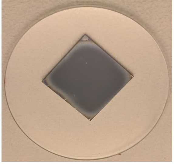
g) After 24 hours, the bond appears homogeneous over the optical aperture of the sample. h)
An anti-reflective coating is applied to the sapphire window via ion beam sputtering (IBS). i)
The SESAM is mounted in a copper cooling mount. The inset shows the full layer structure
of the fabricated sapphire SESAM. j) Picture of the complete device.
The surfaces are made hydrophilic using UV/Ozone cleaning in a custom-built enclosure.
This differs from the usual cerium oxide scrubbing procedure as the SESAMs cannot tolerate it.
UV/Ozone cleaning uses 185-nm and 254-nm light to generate oxygen radicals that react with
organic species adsorbed on the surfaces and turns them into gas that desorb in the atmosphere
[30]. The resulting surfaces have the cleanliness required for successful bonding.
The surfaces are first cleaned with reagent grade acetone and methanol. The samples are then
placed in the cleaning enclosure, and the low-pressure mercury bulbs are started (Fig. 1(b)). For
the first 11 minutes, both wavelengths are produced to fill the box with ozone (up to 200 ppm)
and catalyze the reaction with the contaminants. Then the 185-nm light is turned off and the
ozone is degraded under the action of 254-nm radiation for an additional 15 min before the box is
safe to be opened again. The samples are then taken to be bonded on a laminar flow bench. The
SESAM is placed on a Teflon support to prevent unwanted bonding should there be any overspill
of bonding solution. A final wipe of the surfaces with high purity methanol (Chromasolv for
High Performance Liquid Chromatography) is carried out. A volume of solution amounting to
0.8 µl/cm2 of bonding area is drawn up with a micropipette and laid on the surface of the SESAM
in a single drop (Fig. 1(c)). The sapphire window is slowly brought into contact to allow the
solution to spread without trapping air bubbles (Fig. 1(d)). The SESAM is maintained roughly atResearch Article Vol. 29, No. 12 / 7 June 2021 / Optics Express 18063 the center by touching the edge of the window but with no added pressure. A 3-dimensional silica network develops through etching, polymerization and dehydration (Fig. 1(e)). After a few minutes, the bond forms with a strength sufficient for the sample to be moved (Fig. 1(f)). A photograph of one of the bonded samples is shown in Fig. 1(g). Sixteen samples were bonded this way using varying thickness of sapphire windows (0.2, 0.3, 0.5 and 3.0 mm). All samples were observed to bond well within a few minutes. The samples were left to cure in ambient atmosphere for ten days. The sapphire windows were then coated with an anti-reflective coating (University of Neuchatel) optimized for 632 nm (
Research Article                                     Vol. 29, No. 12 / 7 June 2021 / Optics Express 18064

a)    Thin-film polarizer   f=800mm            b)                     c)
                                                                                          0.10

                                                                     dFth/dPabs (1/m/W)
Half-wave                                                                                 0.05
plate
             Power                                                                        0.00
             meters
                                                                                          -0.05                        Simulation
                                                                                                                       Experiment
                                      Sample                                              -0.10

Interfero-   4f imaging       Camera                                                              0.0        1.0       2.0        3.0
meter                                                                                                   Sapphire thickness (mm)

d)

       Fig. 2. a) The setup used to measure the thermal lens of the SESAMs as a function of
       incident power. The cw laser beam is attenuated with a half-wave plate and thin-film
       polarizer, and focused onto the sample using a lens. The sample surface is measured
       through a 2” mirror close to the sample using an interferometer. b) Measured deviation
       from cold for a sapphire SESAM at 160 W incident power. The black circle indicates the
       1.6-mm-radius-disk used to compute the local curvature. c) Strength of the thermal lens
       dFth /dPabs as a function of sapphire thickness. Experimental data points are measured
       with our interferometer-based setup and the theoretical curve was computed with our finite
       element model. d) Schematic of the finite element model showing the deformation assuming
       5 W of absorbed power (to make the deformation visible, it is scaled up by ×5000) for
       a standard SESAM with no sapphire (left) and a SESAM with a 3.0 mm (right) sapphire
       window bonded on top. The grey and blue lines indicate the outline of the undeformed and
       deformed structure, respectively. The temperature profile is indicated by the contours and
       shows that the heat is concentrated in the absorber region of the SESAM. The 1/e2 width of
       the laser beam is shown in red. The curves at the top show the optical phase picked up by
       the beam as a function of radial position.
Research Article Vol. 29, No. 12 / 7 June 2021 / Optics Express 18065 the interface material also for the standard SESAM, which is usually soldered onto the copper heatsink. The heat is assumed to be entirely generated within the QW section with a Gaussian intensity profile. Figure 2(d) shows the computed deformation (scaled up by ×5000) and temperature profile for 5 W of absorbed power, for the case of no sapphire (left) and a 3.0 mm thick sapphire window (right). These 5 W of absorbed power correspond to the operating point of the SESAM at the highest output power in our high-power mode-locking experiments discussed in the next section. The curves at the top show the optical phase picked up by the laser beam as a function of radial position. As can be seen, a standard SESAM will lead to a defocusing lens due to the thermal expansion of the GaAs substrate. For the sapphire SESAM on the other hand, the resulting lens will be focusing due to two effects: First, the thermal expansion of the sapphire will press the SESAM inwards, and second, the positive thermo-optic coefficient of sapphire leads to an additional focusing lens due to the temperature profile within the window. We repeat the analysis done on the experimental results to extract the slope dFth /dPabs of the thermal lens for different thicknesses of the sapphire window and plot the result in Fig. 2(c) (solid red line). We see good qualitative agreement between the experimental results and the theoretical predictions in Fig. 2(c). The quantitative agreement is reasonable given the lack of any fitting parameters in the model. The thermal lens is being overestimated by the model however, especially for the SESAM with a 3.0 mm sapphire window. Importantly however, the model correctly predicts that the strength of the thermally induced lens, including its sign, can be tuned by changing the sapphire thickness. It is in principle possible to obtain a SESAM with no overall thermal lensing when choosing the appropriate thickness for the sapphire window. In fact, we achieve approximately a two-fold reduction in thermal lensing for the SESAMs with 0.2 mm and 0.3 mm sapphire windows compared to standard SESAMs soldered to a copper heatsink. 4. High-power mode-locked operation 4.1. Thin-disk laser cavity We use the SESAMs in a high-power TDL cavity to verify their suitability for high-power ultrafast operation. The cavity (Fig. 3(a)) is based on previous designs from our group [10]. It incorporates an active multipass cell [32] with three passes on the Yb-doped thin-disk (TRUMPF, see also Fig. 3(b), highlighted gray region), enabling the use of a 30% output coupler to optimize output power. A thin-film polarizer is used to select the polarization. To initiate and stabilize mode-locking, we insert a SESAM as end-mirror. As we rely on soliton mode-locking [33], we balance the self-phase-modulation (SPM) with negative group-delay-dispersion (GDD). The amount of SPM is reduced by partially evacuating the vacuum chamber that contains the laser cavity. To balance the residual SPM picked up by the pulses, four dispersive mirrors with 2× −550fs2 (Layertec) and 2× −2000fs2 (University of Neuchatel) are used, providing a total of −30600 fs2 GDD per roundtrip. Both types of dispersive mirrors support 100 fs pulses. The cavity reaches up to 220 W output power in cw operation, and up to 160 W in mode-locked operation when using a state-of-the-art SESAM grown in-house and contacted by TRUMPF. To reach optimal efficiency while maintaining single-mode operation, the size of the cavity mode (Fig. 3(b)) must be scaled to the size of the pump spot on the disk. The ideal ratio is typically reached with the cavity mode being around 70–80% the size of the pump spot depending on the particular cavity and pump profile [34,35]. However, the exact mode size on the disk (see Fig. 3(b), highlighted red points) depends on the thermal lensing of the intracavity components. In Fig. 3(c), we show the dependence of this mode size as a function of the thermal lens on the disk ∆Fth,disk (solid blue line). As can be seen, the cavity is designed such that it operates around the center of its stability zone with respect to thermal lensing. To illustrate the role of the additional thermal lens of the SESAM, we set its thermal lens to a fixed multiple of ∆Fth,disk . As shown in Fig. 3(c), the shape of the stability zone depends strongly on the lens ratio
Research Article                                                       Vol. 29, No. 12 / 7 June 2021 / Optics Express 18066

  a) SESAM                                  b)                        Disk                    c)            2.2
                                                                      SESAM                                          Higher powers
                                                            2.0                                             2.0

                                           Mode Size (mm)
                                                                                                            1.8
                                                            1.5

                                                                                               wDisk (mm)
   Vacuum-                                                                                                  1.6
   chamber                       GTI                                                                                                Lens ratio
                                                            1.0                                             1.4                         +1.5
                                   thin-                                                                    1.2                           0.0
            GTI                                             0.5                                                                          -1.5
                                   disk                                                                                                  -3.0
                                                                                                            1.0
  OC TFP                                                                                                                                 -4.5
                                 GTI                        0.0
                                                                  0     4       8     12                          -0.08      -0.04      0.00
                                                                         Position (m)                                     ΔFth,disk (1/m)

        Fig. 3. a) The cavity used for the mode-locking experiments. It includes three passes
        on the thin disk, a thin-film polarizer for polarization control and dispersive mirrors for
        dispersion control. The cavity is built inside a vacuum chamber to control the air pressure.
        b) Evolution of the 1/e2 cavity mode radius. The region highlighted in gray indicates the
        multipass scheme on the disk. The red points indicate the disk. c) The cavity mode size
        on the disk as a function of the thermal lens on the disk, for several values of the lens
        ratio ∆Fth,SESAM /∆Fth,disk , i.e. the ratio between the SESAM’s thermal lens and the disk’s
        thermal lens. The highlighted orange curve indicates a favorable lens ratio leading to a
        widening of the stability zone.

∆Fth,SESAM /∆Fth,disk . For values around −3.0 (highlighted, orange), the thermal lenses partially
counteract each other. This in turn leads to a significant widening of the stability zone, extending
the range of thermal lenses where there is a suitable spot size in the thin disk.

4.2.    High power mode-locked operation
We tested SESAMs with four different thicknesses of sapphire (0.2, 0.3, 0.5 and 3.0 mm) and
one standard SESAM without sapphire window. After slightly adjusting the cavity to locate a
spot on the SESAM with favorable cold curvature, we achieve stable mode-locking over a wide
range of output powers, reaching more than 160 W in all cases. For increasing output powers,
the pulse duration decreases as expected for soliton pulse shaping. Hence, to keep the pulse
duration within a suitable range for stable mode-locking, we reduce the intra-cavity air pressure
to optimize mode-locking stability for higher powers. We verify fundamental mode-locking
using the standard mode-locking diagnostics: We record the optical spectrum of the pulses, the
auto-correlation trace using a 200-ps long-range autocorrelator, an oscilloscope trace using a
45-GHz sampling oscilloscope, and the micro-wave spectrum of the pulse train. In Fig. 4(a),
we show the average output power as a function of pump power both for the standard SESAM
(red squares) and for the SESAM with 3.0 mm sapphire (blue circles): We reach a maximum
average output power of 233 W using a SESAM with a 3.0 mm sapphire window, which is a
70-W-improvement over the standard SESAM. The mode-locking diagnostics are displayed in
Fig. 4(b)–4(e) and show a repetition rate of 10.2 MHz with a pulse duration of 734 fs assuming
sech2 pulses, corresponding to a time-bandwidth product of 1.13 × 0.315. The air pressure in the
laser cavity was 166 mbar. We attribute the improved output power to the compensation of the
thermal lenses of the SESAM and disk. In fact, based on our extra-cavity measurements of the
thermal lenses, we estimate the lens ratio to be ∆Fth,SESAM /∆Fth,disk ≈ −2.9, which is very close
to the favorable ratio suggested by Fig. 3(c) (highlighted orange line). This shows that a non-zero
thermal lens of the SESAM can in fact lead to a performance improvement if it counteracts the
lens of the disk. These results demonstrate the flexibility of the sapphire bonded SESAMs: with
an optimal choice of the thickness of the sapphire, a large fraction of the thermal lens of the
active medium or other components can be compensated.
Research Article Vol. 29, No. 12 / 7 June 2021 / Optics Express 18067
b) d) 0
λFWHM= f rep=
Intensity (dBc)
Intensity (a.u.)
a) -20 10.2MHz
1.7nm
250 Standard
Sapphire -40
Output power (W)
200 -60
1025 1030 1035 10.17 10.20
150 Wavelength (nm) Frequency (MHz)
c) e)
0
100 τP=
Intensity (dBc)
Intensity (a.u.)
-10
734fs
50 -20
-30
200 400 600 -40
Pump power (W) -4 -2 0 2 4 50 100 150
Delay (ps) Frequency (MHz)
Fig. 4. a) The average output power as a function of pump power for a standard SESAM (red
squares) and a SESAM with a 3.0-mm sapphire on top (blue circles). b)-e) Mode-locking
diagnostics for the highest output power of the sapphire SESAM (highlighted on the left).
Shown are the autocorrelation trace (b), optical spectrum of the pulses (c), microwave
spectrum of the pulse train around the repetition rate of the cavity (d) and over a broader
range (e).
4.3. Outlook on further power scaling
While achieving the high-power results presented here, we have not observed any damage to
the silicate bond. Hence, we anticipate significant potential for power scaling using this new
SESAM technology. For our record average power TDL oscillator results we used a much larger
pump spot size than used here (6 mm instead of 3.6 mm), which enabled scaling up to 350 W
[1]. The power achievable in that case appeared to be limited by SESAM thermal lensing which
brought the cavity out of the optimal laser-to-pump spot size ratio. Hence, our results here
represent a very promising path to further power scaling. To realize this potential, the design
of the SESAM needs to be adjusted to support higher pulse energies. The devices presented
here use semiconductor layers on top of the absorbers to reduce the fluence in the quantum
wells. Further increasing the number of semiconductor layers would lead to a prohibitively strong
inverse saturable absorption, limiting pulse energy. Thus, we plan to replace the semiconductor
layers with a dielectric top-coating (DTC) [36]. Since using a DTC implies a change in the
top-most material, the bond and/or DTC design will have to be adapted to maintain a high bond
quality.
5. Conclusions
We demonstrate a new method to fabricate high-power compatible SESAMs with an adjustable
thermal lens by bonding sapphire to the front side. We use the fabricated SESAMs to mode-lock
a high-power TDL and reach 233 W of average power. We attribute the improvement of 70 W
compared to a standard SESAM in the same cavity to the compensation of the thermal lenses
inside the cavity. The strength of the thermal lens can be adjusted by changing the thickness
of the sapphire. This control enables optimization of SESAM for different cavities, and the
creation of an “athermal” SESAM with no overall thermal lensing. Another possibility is to use
a strongly wedged sapphire window to allow continuous tuning of the sapphire thickness on aResearch Article Vol. 29, No. 12 / 7 June 2021 / Optics Express 18068
single sample. We discuss potential further improvements to the SESAMs to reach even higher
powers such as including a dielectric top-coating. The bonding method is highly flexible and can
be performed at room temperature, making it applicable to a wide range of materials and devices.
The resulting bond is well-suited for intra-cavity components in high peak-intensity applications.
One potential future application is the creation of high-power or monolithic Vertical External
Cavity SEmiconductor Lasers (VECSELs).
Funding. Science and Technology Facilities Council (ST/N005422/1, ST/V001736/1); Schweizerischer Nationalfonds
zur Förderung der Wissenschaftlichen Forschung (200020_172644).
Acknowledgments. The ETH Zurich authors would like to thank Prof. Martin M. Fejer for helpful discussions in
the early stages of the project. Additionally, we would like to thank Alexander Nussbaum-Lapping and Marco Gaulke for
help with some of the characterization measurements. We also thank Dr. Valentin Wittwer, Dr. Olga Razskazovskaya,
and Prof. Dr. Thomas Südmeyer (University of Neuchatel) for coating the sapphire windows and providing some of
the dispersive mirrors. The University of Glasgow authors would like to acknowledge our colleagues in the Institute
of Gravitational Research, LIGO Scientific Collaboration, the GEO600 project and the Scottish Universities Physics
Alliance for their interest in the work. The authors would like to thank the University of Glasgow and the Science and
Technology Facilities Council for their financial support.
Disclosures. The ETH Zurich authors signed an NDA with TRUMPF with regards to the thin-disk module and head.
Data availability. Data underlying the results presented in this paper are not publicly available at this time but may
be obtained from the authors upon reasonable request.
References
1. F. Saltarelli, I. J. Graumann, L. Lang, D. Bauer, C. R. Phillips, and U. Keller, “Power scaling of ultrafast oscillators:
350-W average-power sub-picosecond thin-disk laser,” Opt. Express 27(22), 31465–31474 (2019).
2. M. Müller, C. Aleshire, A. Klenke, E. Haddad, F. Légaré, A. Tünnermann, and J. Limpert, “10.4 kW coherently
combined ultrafast fiber laser,” Opt. Lett. 45(11), 3083–3086 (2020).
3. P. Russbueldt, T. Mans, J. Weitenberg, H. D. Hoffmann, and R. Poprawe, “Compact diode-pumped 1.1 kW Yb:YAG
Innoslab femtosecond amplifier,” Opt. Lett. 35(24), 4169–4171 (2010).
4. J.-P. Negel, A. Loescher, A. Voss, D. Bauer, D. Sutter, A. Killi, M. A. Ahmed, and T. Graf, “Ultrafast thin-disk
multipass laser amplifier delivering 1.4 kW (4.7 mJ, 1030 nm) average power converted to 820 W at 515 nm and 234
W at 343 nm,” Opt. Express 23(16), 21064–21077 (2015).
5. U. Keller, K. J. Weingarten, F. X. Kärtner, D. Kopf, B. Braun, I. D. Jung, R. Fluck, C. Hönninger, N. Matuschek,
and J. Aus der Au, “Semiconductor saturable absorber mirrors (SESAMs) for femtosecond to nanosecond pulse
generation in solid-state lasers,” IEEE J. Sel. Top. Quantum Electron. 2(3), 435–453 (1996).
6. J. Brons, V. Pervak, E. Fedulova, D. Bauer, D. Sutter, V. Kalashnikov, A. Apolonskiy, O. Pronin, and F. Krausz,
“Energy scaling of Kerr-lens mode-locked thin-disk oscillators,” Opt. Lett. 39(22), 6442–6445 (2014).
7. C. J. Saraceno, F. Emaury, C. Schriber, A. Diebold, M. Hoffmann, M. Golling, T. Sudmeyer, and U. Keller, “Toward
Millijoule-Level High-Power Ultrafast Thin-Disk Oscillators,” IEEE J. Select. Topics Quantum Electron. 21(1),
106–123 (2015).
8. S. Piehler, T. Dietrich, P. Wittmüss, O. Sawodny, M. A. Ahmed, and T. Graf, “Deformable mirrors for intra-cavity
use in high-power thin-disk lasers,” Opt. Express 25(4), 4254–4267 (2017).
9. A. Diebold, T. Zengerle, C. G. E. Alfieri, C. Schriber, F. Emaury, M. Mangold, M. Hoffmann, C. J. Saraceno, M.
Golling, D. Follman, G. D. Cole, M. Aspelmeyer, T. Südmeyer, and U. Keller, “Optimized SESAMs for kilowatt-level
ultrafast lasers,” Opt. Express 24(10), 10512–10526 (2016).
10. I. J. Graumann, F. Saltarelli, L. Lang, V. J. Wittwer, T. Südmeyer, C. R. Phillips, and U. Keller, “Power-scaling of
nonlinear-mirror modelocked thin-disk lasers,” Opt. Express 27(26), 37349–37363 (2019).
11. F. Saltarelli, A. Diebold, I. J. Graumann, C. R. Phillips, and U. Keller, “Modelocking of a thin-disk laser with the
frequency-doubling nonlinear-mirror technique,” Opt. Express 25(19), 23254–23266 (2017).
12. D .-H. Gwo, Two unique aspects of gravity probe-B star-tracking space telescope: (1) focal-plane roof-edge diffraction
and (2) fused-quartz bonding for 2.5-Kelvin applications (SPIE, 1998).
13. R. Douglas, A. A. V. Veggel, L. Cunningham, K. Haughian, J. Hough, and S. Rowan, “Cryogenic and room
temperature strength of sapphire jointed by hydroxide-catalysis bonding,” Class. Quantum Grav. 31(4), 045001
(2014).
14. S. Sinha, K. E. Urbanek, A. Krzywicki, and R. L. Byer, “Investigation of the suitability of silicate bonding for facet
termination in active fiber devices,” Opt. Express 15(20), 13003–13022 (2007).
15. A.-M. A. van Veggel and C. J. Killow, “Hydroxide catalysis bonding for astronomical instruments,” Adv. Opt. Technol.
3(3), 293–307 (2014).
16. B. P. Abbott, R. Abbott, T. Abbott, M. Abernathy, F. Acernese, K. Ackley, C. Adams, T. Adams, P. Addesso, and R.
Adhikari, “Observation of gravitational waves from a binary black hole merger,” Phys. Rev. Lett. 116(6), 061102
(2016).Research Article Vol. 29, No. 12 / 7 June 2021 / Optics Express 18069
17. V. Mangano, A. A. van Veggel, R. Douglas, J. Faller, A. Grant, J. Hough, and S. Rowan, “Determination of the
refractive index and thickness of a hydroxide-catalysis bond between fused silica from reflectivity measurements,”
Opt. Express 25(4), 3196 (2017).
18. G. Lacaille, V. Mangano, A.-M. A. van Veggel, C. J. Killow, P. E. MacKay, S. Rowan, and J. Hough, “Optical
characterisation of hydroxide catalysed bonds applied to phosphate glass,” in Optifab 2017(International Society for
Optics and Photonics 2017), p. 1044825.
19. G. T. Nick and R. C. Neil, “Improved bond strength characterization of chemically activated direct bonding (CADB)
epoxy-free bonded solid state laser materials,” in Proc.SPIE(2010).
20. M. De Vido, D. Meissner, S. Meissner, K. Ertel, P. J. Phillips, P. D. Mason, S. Banerjee, T. J. Butcher, J. M. Smith,
and C. Edwards, “Characterisation of adhesive-free bonded crystalline Yb: YAG for high energy laser applications,”
Opt. Mater. Express 7(2), 425–432 (2017).
21. K. S. Prabhu, T. L. Schmitz, P. G. Ifju, and J. G. Daly, “A survey of technical literature on adhesive applications for
optics,” in New Developments in Optomechanics (International Society for Optics and Photonics 2007), p. 666507.
22. C. Y. Sheng, “Effects of laser-induced damage on optical windows in the presence of adhesives under simulated
thermal-vacuum conditions,” in Laser-Induced Damage in Optical Materials: 2006 (International Society for Optics
and Photonics 2007), p. 64030H.
23. K. Fujioka, A. Sugiyama, Y. Fujimoto, J. Kawanaka, and N. Miyanaga, “Ion diffusion at the bonding interface of
undoped YAG/Yb: YAG composite ceramics,” Opt. Mater. 46, 542–547 (2015).
24. I. Mukhin, E. Perevezentsev, and O. Palashov, “Fabrication of composite laser elements by a new thermal diffusion
bonding method,” Opt. Mater. Express 4(2), 266–271 (2014).
25. A. Berthold, L. Nicola, P. Sarro, and M. Vellekoop, “Glass-to-glass anodic bonding with standard IC technology thin
films as intermediate layers,” Sens. Actuators, A 82(1-3), 224–228 (2000).
26. C. J. Killow, E. D. Fitzsimons, J. Hough, M. Perreur-Lloyd, D. I. Robertson, S. Rowan, and H. Ward, “Construction
of rugged, ultrastable optical assemblies with optical component alignment at the few microradian level,” Appl. Opt.
52(2), 177–181 (2013).
27. D. -H. Gwo, “Hydroxide-catalyzed Bonding,” (The Board of Trustees of the Leland Stanford Junior University
(Stanford, CA), 2003).
28. Y.-L. Sun, Y.-X. Ye, X.-H. Shi, Z.-Y. Wang, C.-J. Yan, L.-L. He, Z.-H. Lu, and J. Zhang, “A hybrid silicon-sapphire
cryogenic Fabry–Perot cavity using hydroxide catalysis bonding,” Class. Quantum Grav. 36(10), 105007 (2019).
29. D. -H. Gwo, “Ultra precision and reliable bonding method,” (The Board of Trustees of the Leland Stanford Junior
University (Stanford, CA), 2001).
30. J. R. Vig, ““UV/ozone cleaning of surfaces,” Journal of Vacuum Science & Technology A: Vacuum,” J. Vac. Sci.
Technol., A 3(3), 1027–1034 (1985).
31. P. Zhang, M. Jiang, R. Zhue, D. Zhang, and Y. Song, “Thermal conductivity of GaAs/AlAs distributed Bragg
reflectors in semiconductor disk laser: comparison of molecular dynamics simulation and analytic methods,” Appl.
Opt. 56(15), 4537 (2017).
32. J. Neuhaus, J. Kleinbauer, A. Killi, S. Weiler, D. Sutter, and T. Dekorsy, “Passively mode-locked Yb:YAG thin-disk
laser with pulse energies exceeding 13 µJ by use of an active multipass geometry,” Opt. Lett. 33(7), 726 (2008).
33. F. X. Kartner, I. D. Jung, and U. Keller, “Soliton mode-locking with saturable absorbers,” IEEE J. Sel. Top. Quan.
Electron. 2(3), 540–556 (1996).
34. A. Diebold, F. Saltarelli, I. J. Graumann, C. J. Saraceno, C. R. Phillips, and U. Keller, “Gas-lens effect in kW-class
thin-disk lasers,” Opt. Express 26(10), 12648–12659 (2018).
35. F. Saltarelli, D. Koenen, L. Lang, I. J. Graumann, C. R. Phillips, and U. Keller, “Beam quality in high-power thin-disk
lasers: influence and measurement of the radial inversion profile,” in Laser Congress 2019 (ASSL, LAC, LS&C)
(Optical Society of America, Vienna, 2019), p. JM5A.35.
36. C. J. Saraceno, C. Schriber, M. Mangold, M. Hoffmann, O. H. Heckl, C. R. E. Baer, M. Golling, T. Südmeyer, and U.
Keller, “SESAMs for high-power oscillators: design guidelines and damage thresholds,” IEEE J. Sel. Top. Quan.
Electron. 18(1), 29–41 (2012).You can also read