Technology Highlights 2018
←
→
Page content transcription
If your browser does not render page correctly, please read the page content below

Industry & Suppliers

 Technology Highlights 2018
 Increments and innovations: Whether a tweak to push
 faster throughputs or higher efficiencies from an already
 proven process, or a bold new step into unknown territory,
 innovation is the force behind solar’s phenomenal growth
 in recent years; and will continue to cement its position as
 a clean and commercially viable source of energy.

                                      The fourth edition of pv magazine’s Tech-   reviewed and ranked 25 entries.
                                      nology Highlights counts down some of       Of these, six were chosen as final-
                                      the top new and improved products and       ists to be further picked over by the
                                      processes from across the upstream sup-     assembled experts who, after plenty
                                      ply chain, from polysilicon production      of discussion and deliberation, selected
                                      down to post assembly module testing,       the technologies named below for recog-
                                      all of which have made a valuable contri-   nition as the top Technology Highlights      year. The recipient of this award will be
                                      bution to boosting solar’s potential, and   of 2018.                                     chosen from the top submissions to mul-
                                      pushing down its prices.                       The six finalists will automatically be   tiple features running throughout the
                                         A jury of experts from across the        candidates for the inaugural pv maga-        year, covering all of the biggest industry
                                      industry, assembled by pv magazine, has     zine award, to be given at the end of the    segments.
     Photo GT Advanced Technologies

                                                                                  Top innovation:
                                                                                  GT Advanced Technologies Polysilicon
                                                                                  Tube Filaments

                                                                                                                                                                               Photo: 3D-Micromac
                                                                                                           Runner up:
                                                                   3D-Micromac Microcell OTF
     Photo: 1366 Technologies

                                                                                  Technology to Watch:
                                                                                  1366 Technologies Direct Wafer Process

                                      pv magazine would like to thank all of the companies that took the time to share details of their latest
                                      innovations with us, and the jury members for sharing their valuable time and considerable expertise.

56                                                                                                                                           05 / 2018 | www.pv-magazine.com
Industry & Suppliers

The Award Jury

Andrew Blakers                                Peter Fath                                   Rainer Gegenwart
Andrew Blakers is a Professor of              Fath is Managing Director of RCT Solu-       As CTO at Phanes Group, Gegenwart is
Engineering at Australian National            tions, and Chair of the Solar Equip-         responsible for a diverse pipeline of PV
University.                                   ment Machine Maker Group at the Ger-         projects with a focus on the Sub-Saharan
His research interests include photovol-      man Engineering Federation (Verband          Africa and MENA regions. Gegenwart
taic and solar energy systems, concentra-     Deutscher Maschinen- und Anlagenbau).        also leads the team to develop off-grid
tor solar cells, components, and systems,     Fath has held senior positions with equip-   and hybrid solar solutions. Previously, he
and sustainable energy policy.                ment makers including Rena GmbH and          was Managing Director at ANTEC Tech-
“One thing that comes out of being            centrotherm, and lectures on manufac-        nology and between 2003 and 2005, he
involved in awards like this is to see that   turing technology in PV at leading insti-    oversaw the setup of First Solar in Ger-
there is no end in sight to the cost reduc-   tutes including the University of Stutt-     many. He also founded cleantech advi-
tions in a silicon solar cell.”               gart and University of Applied Science,      sory and project development company
                                              Ravensburg.                                  Heliosmax in 2010.

Pierre J. Verlinden                           Xiaoting Wang                                Edurne Zoco
Verlinden is Managing Director of PV          Xiaoting Wang is an Energy Specialist        Edurne Zoco is Research Director, Solar
consulting firm Amrock. Verlinden has         at Bloomberg New Energy Finance, and         & Energy Storage at IHS Markit. Her
worked in PV for more than 39 years,          has been conducting research into the PV     main focus areas include module intel-
and published over 200 technical papers.      industry since 2012.                         ligence services, which track PV manu-
From 2012 to 2018, he was Vice President      In total, Xiaoting has published more        facturing trends and monitor the module
and Chief Scientist at Trina Solar, and       than 100 insight notes. The scope of         and polysilicon supply chain to develop
Vice Chair of the State Key Laboratory        her research and expertise covers the        detailed analysis and projections.
of PV Science and Technology. Verlinden       global PV supply chain, including sup-       Zoco has been involved in solar for more
recieved the 2016 William Cherry Award,       ply-demand relationships, cost and           than a decade, offering insights and mar-
from the Institute of Electrical and Elec-    price variations, technological progress,    ket data to develop company individual
tronic Engineers (IEEE), one of the high-     and the impacts of international trade       growth strategies, market entry plans,
est distinctions in PV research.              disputes.                                    and competitive analysis.

           05 / 2018 | www.pv-magazine.com                                                                                              57
Industry & Suppliers

      1        GT Advanced Technologies Polysilicon Tube Filaments
               Reducing energy consumption and increasing productivity

      GT Advanced Technologies (GTAT)                 five times greater than typical thin sili-    Jury Comments
      is bringing its Tube Filaments to the           con filaments. Increasing the surface area    • “This approach to designing the fila-
      polysilicon production market, a solu-          five times, says GTAT, shortens the depo-       ments is quite smart, and overcomes
      tion which it says can reduce the energy        sition growth cycle and allows the depo-        quite some issues in polysilicon deposi-
      needed in Siemens process polysilicon           sition to operate at a highly efficient and     tion efficiency.”
      production by as much as 20%, while             productive level throughout the growth        • “A new deposition base for more effi-
      increasing annual production rates by           cycle.                                          cient polysilicon growth replaces the
      more than 30%.                                     A further benefit outlined by GTAT           old setting and is easy to operate. It
         According to GTAT, the tube filaments        is improved reliability, and reduction          could become a new standard for the
      function as a direct replacement for the        in early run aborts: “The hollow design         industry.”
      standard filaments used in any Siemens          of Tube Filaments enhances reliabil-
      process reactor. This means that manu-          ity at the end of the run by allowing for

                                                                                                                                                    Photos: GT Advanced Technologies
      facturers will be able to take advantage of     large rod diameters without risk of melt-
      the improved performance, without any           ing, and eliminating rod stress,” GTAT
      disruption to their production, or any          explains. The structure of the filaments
      need to invest in expensive new machin-         also enables them to be made taller with-
      ery. The company claims that by leverag-        out the risk of leaning or swaying, further
      ing all of the benefits of its tube filaments   increasing productivity.
      solution, capacity improvements of 75%             The company offers its Tube Filaments
      or higher are possible on existing produc-      directly to polysilicon suppliers as a con-
      tion equipment.                                 sumable with immediate benefits to
         Key to the innovation is the Tube Fil-       polysilicon production with zero capi-
      ament’s increased surface area, which is        tal outlay.

58                                                                                                                05 / 2018 | www.pv-magazine.com
Industry & Suppliers

                 2           3D-Micromac microCELL OTF 8000
                             Upgraded dual line laser processing system for Si cells

                     3D-Micromac’s microCELL OTF 8000             pared to the previous machine version.         technology for unbeaten throughput
                     is a versatile laser system for process-     Moreover, it fits better with in-line inte-    remain. The tool uses laser sources only.
                     ing of mono and multicrystalline sili-       gration into print lines or to comparable      The standard used are 1064 nm wave-
                     con wafers, including latest technologies    long process cycle times like doping.          length ns-fibre lasers, with the option
                     like laser contact opening for PERC cells      The operator can easily change between       to equip the tool with customer speci-
                     or doping. It is an upgraded version of      different patterns (line, dot, dash, or cus-   fied solutions, including different wave-
                     the previous tool microCELL OTF 3600,        tomized) and select laser parameters with      lengths, pulse duration, or source manu-
                     embedded with new HMI functions and          a drop-down/value input feature. The           facturer on request.
                     extra hardware options.                      benefits of contactless wafer transport on        3D-Micromac mentions that partic-
                        The critical feature of OTF 8000 is       an air cushion, supporting also the fur-       ular attention was paid to designing
                     that it is advanced to a two-lane design,    ther decrease in nominal cell thickness,       the air management with the exhaust.
                     allowing for double the throughput.          and the fire on-the-fly high scan speed        Apart from health and safety measures,
                     Both lanes work independently of each                                                       the control of dust removal is raised to
                     other. 3D-Micromac claims that with the                                                     tighten the process control without acci-
                     increased throughput to 8,000 wafers per                                                    dental loss of laser power in the dust
                     hour the cost has not been doubled, com-                                                    cloud above the substrate.
Photo: 3D-Micromac

                                                                                                                 Jury comments:
                                                                                                                 • “A great innovation to improve through-
                                                                                                                   put and reduce COO of laser ablation
                                                                                                                   for PERC cells. 8000 UPH with no-con-
                                                                                                                   tact transport is very impressive.”
                                                                                                                 • “The wafer is processed as it is trans-
                                                                                                                   ferred from one end to the other of the
                                                                                                                   machine. I think that’s an excellent
                                                                                                                   idea: Higher throughput means fewer
                                                                                                                   laser heads per line.”

                                05 / 2018 | www.pv-magazine.com                                                                                              59
Industry & Suppliers

      3        1366 Technologies Direct Wafer Process
               Multi wafer with zero kerf and cutting

      Now well on the way toward large-scale commercialization, the

                                                                                                                                                 Photos: 1366 Technologies
      patented Direct Wafer Process developed by 1366 Technologies
      is an alternative method for wafer manufacturing which exhib-
      its various advantages over traditional cast and saw methods,
      and could bring about major cost reductions to wafering – one
      of the most expensive stages in PV production.
         According to 1366, the current technology cuts costs to $0.26
      per wafer, around half that of leading manufacturers using the
      traditional process, and the company’s technical road map
      could bring this down even further to $0.15/wafer.
         The process creates standard silicon wafers directly from
      molten silicon, which, as well as reducing waste from kerf,
      offers several other advantages. Wafers created this way can be
      designed in 3D – extremely thin to reduce material consump-
      tion, but with thicker, reinforced sections where needed.              Highlights for 1366 Technologies over the past year include
         The company also states that wafers made this way benefit        achieving an average cell efficiency of 20.3% with partner
      from higher purity, and better, more uniform microstructures.       Hanwha Q CELLS, the completion of the first commercial
      The technology also provides the opportunity to manipulate          installation featuring wafers made with the Direct Wafer Pro-
      dopant concentration – potentially a powerful tool in boost-        cess – a 500 kW array in Japan, and the beginning of work on
      ing cell efficiency.                                                its first commercial factory in Southeast Asia.
         “Today’s wafer manufacturing processes are based on 40
      and 50 year old technologies. While incremental improve-            Jury comments:
      ments (such as diamond wire sawing) and economies of scale          • “It is a wonderful innovation, though there are still some prob-
      bring some cost reduction, ingot-based wafer manufacturing            lems to overcome before implementing it in production.”
      has inherent efficiency and cost limitations,” says 1366 Technol-   • “The approach is very novel – if they can reach the goals they
      ogies. “The Direct Wafer manufacturing process fundamentally          have set it would really be a big decline in wafer prices.”
      changes the role of the wafer in the silicon value chain. New       • “The Direct Wafer approach fundamentally changes the way
      wafer features, impossible through wire sawing, can bring fur-        wafers are produced, and leads to lower energy and material
      ther cost reduction and efficiency gains.”                            consumption.”

60                                                                                                             05 / 2018 | www.pv-magazine.com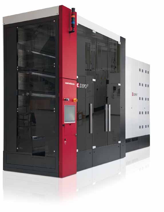
Industry & Suppliers

4       Meyer Burger DW291
        Next generation diamond wire saw platform

                                                                                                                                                 Photo: Meyer Burger
The introduction of diamond wire saw-       Series 3, including a completely rede-
ing to PV production was a massive step     signed drive train, which increases load
in bringing down the costs of PV produc-    length by 28%, and an improved motor
tion, and indeed, Meyer Burger’s origi-     which allows the tool to operate at higher
nal diamond wire platform was the top       speeds and achieve its increased capacity.
ranked innovation back in 2016’s Tech-         Meyer Burger has also been able to
nology Highlights.                          reduce the amount of diamond wire
   Now, with its new DW291 platform, the    consumed, through an innovative new
Swiss equipment provider is introducing     management system. Through optimized
a series of innovations to further reduce   pulleys and a new machine structure,
the cost of wafer production, through       unguided wire length and tension fluc-         Jury Comments:
reduced material consumption, conver-       tuations are reduced, allowing the tool to     • “The diamond wire tool is feasible for
sion cost, and resources deployed.          cut using a 50 micron diamond wire, and          mono and multi c-Si, and requires 25%
   DW291 utilizes diamond wires just        use only 0.8 meters of diamond wire to           less equipment for the line – in terms of
50 microns thick, with an upgrade path      slice wafer, in comparison to other tools        capex that’s very interesting. In terms of
to 40 microns, and can produce wafers       which require more than 1 meter.                 demand, I think this equipment fits the
as thin as 100 microns (mono c-Si) and         The company estimates that the thin-          market at the moment.”
140 microns (multi c-Si). The tool boasts   ner diamond wire it is working can save        • “Diamond wire has been such a huge
a 50 MW throughput – increased by 43%       0.6 grams of silicon per wafer sliced, lead-     success already – it will probably reach
from 35 MW in the previous iteration.       ing to 4% more production from the same          100% of production next year. From
   The tool boasts several major inno-      amount of material (based on 180 micron          what I read here from Meyer Burger,
vations over its predecessor the DW288      wafer thickness).                                it’s a great incremental innovation.”

                                                                                                                                 Advertisement
Industry & Suppliers

                          5       centrotherm c.DEPO LP LPCVD system
                                  Bringing high efficiency to mass production

                          The c.DEPO LP from German supplier          niz Universtität Hannover and the Insti-         Centrotherm points out that, while
                          centrotherm is a high throughput system     tute for Solar Energy Research Hamelin        p-type wafer currently has a market share
                          for the deposition of passivated contacts   (ISFH) to create a p-type monocrystal-        of more than 90%, conversion efficiencies
                          on p-type silicon wafer. The tool works     line cell of 26.1% conversion efficiency –    in excess of 25% have so far only been
                          on a batch-type production, which cen-      a world record for a cell of such material.   achieved using n-type silicon wafers,
                          trotherm says offers advantages in terms       The tool, according to centrotherm,        which will require significant invest-
                          of flexible production load, varying pro-   achieves excellent passivation quality        ments in new equipment and processes to
                          cess sequences, and continued operation     in two ways: through a thin interfacial       ramp up. The company points to its col-
                          in case of single tube maintenance, shut-   oxide (1.3-2.4 nanometers) leading to low     laboration with leading German research
                          down of process optimization.               recombination loss at the surface, and        institutes as evidence that its technology
                            The low pressure chemical vapor           moving the highly doped area from the         enables cost-effective, very high efficien-
                          deposition (LPCVD) process utilized by      c-Si substrate into the poly-Si on top of     cies using p-type silicon wafer.
                          c.DEPO was used in February by Leib-        the thin interface oxide.
                                                                                                                    Jury comments:
                                                                                                                    • “This tool offers the potential for a sub-
                                                                                                                      stantial increase in cell efficiency, which
                                                                                                                      propagates over the entire value chain.”
Photo: centrotherm

   62                                                                                                                              05 / 2018 | www.pv-magazine.com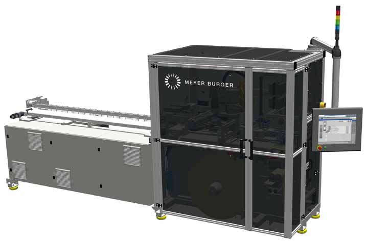
Industry & Suppliers

6        Meyer Burger SWCT Stringer
         Cell connection beyond busbars

Meyer Burger’s SWCT stringer boasts a        PERT modules, and by up to 75% for het-      resents a completely new approach to
throughput of 1,666 cells per hour on a      erojunction technology.                      holding cells in place for stringing, and
footprint of 10 m², adding up to 130 MW        The round wires used in SWCT also          does not use mechanical stress and par-
annual capacity, which Meyer Burger          reduce shading on the active cell surface    tial stress, but rather applies a uniform on
says makes it the smallest stringer avail-   by up to 25% compared with standard          the surface of the cell.
able in the industry.                        busbar technologies, says Meyer Burger,
  The stringer utilizes a new approach to    due to the sunlight being reflected on the   Jury Comments:
grip and hold the cells during stringing.    round surface and back into the mod-         • “This tool offers several notable advan-
The nature of the SmartWire cell con-        ule. In December 2017, Meyer Burger            tages over traditional metallization
nection technology (SWCT) means that         announced it had achieved a 335 W              processes.”
no additional components are required,       power output on a heterojunction mod-        • “The SmartWire technology is very
other than the cells and the foil wire       ule utilizing SWCT.                            innovative, but what I see in the indus-
assembly.                                      SWCT can also boost a module’s life-         try is everybody moving in the direction
  Seen by many as the next step in cell      time and durability, by creating a dense       of multiwire, rather than smartwires.”
interconnection, SWCT utilizes a foil        wire contact matrix on the cell, able to
wire electrode to connect cells, greatly     cope with increased power extraction.
reducing the consumption of costly silver      Meyer Burger states that the gripper
in cell production by up to 65% in PERC/     technology utilized in this stringer rep-

                                                                                                                                         Photo: Meyer Burger

           05 / 2018 | www.pv-magazine.com                                                                                                                     63
Industry & Suppliers

                       7        Innolas Solutions Laser Direct Cleaving

                                                                                                                                                                   Photos: Innolas Solutions
                                Zero ablation cell cutting from Innolas Solutions

                       With many tier-1 manufacturers mov-           ufacturers to increase module power
                       ing into commercial production of half-       output without radically altering their
                       cut cell technology, plenty of attention is   production setup.
                       currently being placed on processes for          German laser specialist Innolas Solu-
                       cell cutting. Using half-cut cells reduces    tions has introduced a cutting process
                       resistive losses, and with the right pro-     named Laser Direct Cleaving, which sep-
                       cess, this can be a simple way for man-       arates the cell using tension created by a
                                                                                                                  laser. The process is entirely ablation free,
                                                                                                                  which, according to the company, results
                                                                                                                  in significant savings by eliminating the
                                                                                                                  need for additional process gas, cooling
                                                                                                                  material, or filtration and dust collection
                                                                                                                  – as no material is removed from the cell
                                                                                                                  during the process.
                                                                                                                    Wafers cut using this process, says
                                                                                                                  Innolas, do not exhibit any weakness or
                                                                                                                  molten areas, resulting in low breakage
                                                                                                                  rates and increased mechanical strength.
                                                                                                                    Innolas Solutions’ Laser Direct Cleav-
                                                                                                                  ing tool can process up to 6,000 wafers
                                                                                                                  per hour, and as well as halves can also
                                                                                                                  dice cells into quarters or any number of
                                                                                                                  pieces in mass production.

                       8        h.a.l.m cetisPV-EL-package
                                Integrated EL measurement and defect detection from h.a.l.m.

                                                                     h.a.l.m.’s cetisPV-EL-package inte-          new tool. Automatic defect detection
                                                                     grates electroluminescence (EL) imag-        algorithms make the system suitable for
Photo: h.a.l.m

                                                                     ing with I-V testing, an innovation          all common cell technologies, including
                                                                     which it says reduces footprint and com-     PERC, HJT, and multicrystalline silicon.
                                                                     ponent requirements in cell production,         The solution facilitates an industry 4.0
                                                                     while providing high quality data on cell    approach, allowing for automated error
                                                                     defects for binning and sorting.             analysis, and introducing combined data
                                                                        The cetisPV-EL-package utilizes the       analysis approaches to the industry by a
                                                                     latest generation of h.a.l.m.’s PVCon-       cell-wise correlation of EL and I-V data.
                                                                     trol-EL-eval 2.0 software for automatic      EL imaging, says h.a.l.m., is ideally suited
                                                                     defect detection and stores EL and I-V       to minimizing downtime and the testing
                                                                     test results in one database, allowing for   required to trace back problems in a pro-
                                                                     combined approaches and analysis cor-        duction line. Integrating EL imaging into
                                                                     relating I-V abnormalities with EL visi-     the I-V testing station removes the need
                                                                     ble defects.                                 for a second contacting of cells, optimizes
                                                                        EL images are acquired in the same        data correlation, and minimizes opera-
                                                                     contacting station as the I-V test and       tor, component, and footprint costs.
                                                                     typically take 120 milliseconds or fewer.
                                                                     This allows for throughput of up to 3,600    Jury Comments:
                                                                     cells/hour on a single lane machine. The     • “A significant improvement in cell char-
                                                                     system is modular, with the possibility to     acterization technology.”
                                                                     upgrade parts such as the camera or I-V
                                                                     tester, without the need for an entirely

                 64                                                                                                              05 / 2018 | www.pv-magazine.com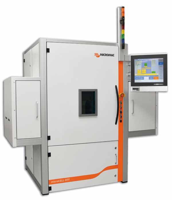
Industry & Suppliers

9       Eternal Sun High Performance Light Soaker
        Temperature control and in situ I-V testing for a better understanding of LID

Eternal Sun’s High Performance Light        With new high efficiency technologies of      Jury comments:
Soaker (HPLS) allows for highly accurate    more responsive external quantum effi-
testing of modules at different tempera-    ciency, issues of LID and LeTID, which        • “An important product for testing
tures to provide reliable representation    though manageable are still widely per-         LID, CID, and LeTID in a controlled
of light-induced degradation (LID), light   ceived as high risk and affect a project’s      environment.”
and elevated temperature induced degra-     bankability, can be mitigated. Eternal
dation (LeTID), and regeneration effects.   Sun states that its HPLS solution allows
   HPLS reduces inaccuracy to 4%, which     users to accurately study a full year’s

                                                                                                                                          Photo: Eternal Sun
the company says represents a 50% gain      degradation, and equally importantly
over comparable solutions. The tool fea-    regeneration, in just seven days, making
tures 350-1200 nm, AAA (IEC60904-9          energy yield predictions more robust.
ed.3) steady state light sources, and an    Based on market feedback, Eternal Sun
integrated temperature chamber with         is aiming to foster a better understanding
temperature stability of +/- 1°C. It also   of LID, LeTID, and regeneration mecha-
allows for real-time I-V measurements       nisms, which heavily depend on irradi-
during light soaking which eliminates       ance and temperature. Studies show that
the need to interrupt light soaking for     these can cause major efficiency losses,
off-line PMAX determination, potentially    particularly in PERC technologies. The
compromising data quality.                  HPLS also aims at improving knowledge
   Investor confidence and risk miti-       of modules’ behaviour in different condi-
gation are two of the biggest factors in    tions, as solar spreads into more locations
allowing solar to continue its growth.      the world over.

                                                                                                                          Advertisement

                 STRINGER TT1600 ECA
                 Advanced adhesive technology for HJT cells

                                                                                                                 VISIT US!
                                                                                                                    May 28-30, 2018
                                                                                                                      Booth E3-365
                                                     Innovative
                                                     Cell Connection
                                                     Technology

                 STRINGER TT1600ECA - A smart solution
                    Innovative string production technology using electrically conductive adhesive (ECA)
                                                                                                            www.teamtechnik.com
                    Reliable process technology with a proven standard STRINGER
                    Ideal for processing HJT high performance cells and busbarless cells
                    Possibility to use light capturing ribbons, LCRTM
                    Lead-free adhesive technology
                    Cost-effective and economical production
Industry & Suppliers
10 Meyer Burger FABiA
3-in-1 machine for anti-reflection, rear, and front passivation processes
FABiA stands for Front and Back in- The new tool is a combination of previ- in a maximized mechanical yield with
line Apparatus. It combines three pro- ous industry renowned machines devel- PERC cells consistently achieving >22%
cesses: anti-reflection coating, and rear oped by Meyer Burger: SiNA, and MAiA. efficiency in mass production. The com-
and front passivation of PERC cells in one The company claims that FABiA, with pany says that FABiA has an average pro-
machine, and offers benefits for future its advanced interfaces and no vacuum duction throughput of over 4,000 wafers
upgrades as a flexible modular system in breakage, provides further improved cell per hour.
mass production. passivation resulting in increased cell The company also claims that with
efficiency and equipment reliability. It is the optimized process, the process gases
Photo: Meyer Burger
also qualified for other technologies like requirement is reduced by 35%. Thanks
PERx, p-type, and n-type covering both to the reduction of two steps, the elec-
mono and multicrystalline wafers. tricity consumption can be reduced by
With this new machine, the manufac- 35%. The overall result is a reduction in
turing footprint is 50% smaller than that the total cost of ownership for PERC cell
of single step equipment, and its fully manufacturers.
automated process sequences simplify
cell production complexity. It saves over Jury comments
1,000 m2 of production floor space per • “With optimized design and the inte-
gigawatt manufactured. gration of three steps, Meyer Burg-
Meyer Burger states that the new er’s new generation tool for PERC pro-
tool minimizes mechanical and opera- cesses is expected to achieve better
tor wafer handling during deposition, economics.”
thus, less cell contamination during the
deposition process. Overall this results
11 RENA BatchTex N
Low footprint, low cost wafer texturing from RENA
RENA Technologies from Germany has line cleaning – a process that uses large processing times. The O3 solution is also
long been a pioneer in the texturing space amounts of hydrogen peroxide (H202), a more environmentally friendly and does
for mono wafers, and this year has a new costly chemical process that has led to not require any poisonous precursor
ozone-based additive called BatchTex N, increased wafer prices. gases, RENA says.
a range of solutions for high throughput The new RENA solution, the BatchTex This critical processing step for high
wafer texturing on a low footprint. N400, which can work with RENA’s exist- efficiency cells ensures a high level of
Previously, wafer conditioning in this ing monoTEX texturing additive, uti- cleanliness before thermal diffusion of
segment had typically been done by alka- lizes instead an ozone (O3) based clean- the p-n junction. By performing this
ing process that is substantially cheaper action using O3, costs can be reduced by
than H202 and is also suitable for shorter around 30%, RENA CEO Peter Schnei-
dewind says. “We are continuing to sup-
Photo: RENA Technologies GmbH
port our customers with such cost-down
measures allowing them to keep up in the
race for ever-declining cell and module
ASPs,” he says. “We expect to see more
and more O3-based processes in this
application as it enables lower operating
expenses in cell fabrication.”
RENA cites cost of ownership calcu-
lations showing costs per wafer can be
reduced to below $0.035/wafer – a saving
of half a million U.S. dollars for a single
200 MW production line annually.
66 05 / 2018 | www.pv-magazine.comIndustry & Suppliers
12
Photo: Ecoprogetti
Ecoprogetti ECOSUN Bifacial
Shedding light on both sides
Ecoprogetti’s ECOSUN Bifacial is an
LED sun simulator designed to simulta-
neously test both sides of a bifacial mod-
ule. The test is carried out in one step,
with no need to move or flip the panel
and repeat. One LED is placed on top of
the module, illuminating at 1,000 W/m²,
and the second unit illuminates the rear
side at between 100 and 1000 W/m².
According to Ecoprogetti, the machine is
suitable for 60, 72, and 90 cell modules
of all commercial technologies, and the
LEDs can perform more than 50 million
pulses at a stable irradiation level with- light conditions including albedo, alti- to handle the module manually, it is able
out the need to recharge in between tests. tude, tilt angle, and reflective surface size. to keep up with the rising throughputs
The machine can be integrated into pro- This, says Ecoprogetti, will allow users to seen in module production today.
duction lines or used as a standalone tes- have a precise idea of power output corre-
ter after shipment to an installation site. sponding to module behavior in particu- Jury comments
ECOSUN Bifacial is fitted with 11 dif- lar conditions. • “Bifacial module testing is gaining
ferent LED types, to best simulate the Ecoprogetti goes on to say that by elim- momentum and is very important. An
full irradiance spectrum of sunlight. The inating any need for recharging between LED Solar Simulator for n-type bifacial
light source provides flexibility, allow- tests, and performing the test of both and all high-efficiency cells is critical. I
ing the machine to replicate site-specific sides simultaneously without any need am glad to see it available.”
13 Singulus Linex DW
In-line texturing process for diamond wire cut multi c-Si
Since the advent of diamond wire sawn results in a cost-effective method on the
Photos: Singulus
wafers first raised its head a few years same footprint as previous iterations of its
ago, developing a solution to the smooth, wet chemical processing platform.
highly reflective surface the saws leave Linex DW also features a newly devel-
behind on multicrystalline wafers has oped conveyor system, which Singulus
been a key priority for solar equipment says guarantees gentle handling through-
suppliers. out, and results in a greatly reduced
Diamond wire sawing is faster than breakage rate (less than 0.05%).
slurry saws, and also produces less waste The tool is designed as a drop-in
and more wafers per silicon block. Pre- replacement for existing wet chemical
viously, the technology had been limited processes, on the same footprint. Linex
to use in monocrystalline silicon, as on DW is available as a 5 or 10 lane tool, with
multi, the saw left behind a surface too rated throughput of 4,200 to 9,000 wafers
smooth and reflective to make a useful per hour.
solar cell. “The texturing of wafers is a step that
In December 2017, Singulus launched has a major influence on the efficiency of
the Linex DW – in-line wet process- the solar cell,” says Singulus CEO Stefan
ing equipment, with an additional new Rinck. “We have equipped the Linex in-
integrated process for diamond wire cut line processing system for wet chemical
wafers. The solution incorporates two dis- surface treatment with the new combined
tinct steps developed inhouse by Singu- process, which means we can bring costs
lus: the use of new additives, and ozone down significantly while also improving
for post cleaning, which the company says cell performance.”
05 / 2018 | www.pv-magazine.com 67Industry & Suppliers
14 Agfa’s UNIQOAT
Single-layer backsheet
UNIQOAT is a PET-based single layer several processing stages, including the enhanced layers. Therefore, according to
backsheet. It requires just one integrated application of an adhesive and a laminate Agfa, UNIQOAT totally eliminates the
process for producing a full backsheet film, curing in a heat chamber for several risk of intra-backsheet delamination.
film, and at no stage in production is days, and repeating for each side. Also, the backsheet has an average adhe-
more than one layer involved. UNIQOAT The new single-layer backsheet has sion to EVA of >100 N/cm.
offers manufacturing advantages over no interlayer lamination, and no coex- Whereas traditional laminated back-
conventional backsheets, which require trusion of different PET grades or other sheet includes a dedicated air-side layer,
UNIQOAT acts as an airside layer in its
full thickness: Even if several microm-
Photo: AGFA
eters were eroded or accidentally dam-
aged, the full thickness of the material is
still hydrolysis and UV resistant.
According to Agfa’s reflectivity mea-
surements, across the entire light-spec-
trum, UNIQOAT performs up to 20%
better than other PET-based materials
chosen by Agfa for comparison (TPT,
TPE, KPE, PPE, and PO – basis: test-
ing 2017). Agfa claims that UNIQOAT’s
high reflectivity – varying with differ-
ent UNIQOAT products – can increase
power output by 0.3 to 0.5%, thus help-
ing to reduce the cost per watt.
15 Tempress SPECTRUM Ox-Poly
LPCVD System for in situ oxidation and deposition of polysilicon layers
Developed by Dutch equipment maker bination due to screen printed metal breaking vacuum. It also provides the
Tempress, part of the Amtech Group, contacts. possibility for doping of the polysilicon
SPECTRUM Ox-Poly is a system for the The tool performs in situ oxidation during deposition, eliminating the need
production of passivated contacts on and subsequent LPCVD polysilicon for a separate dopant diffusion step.
crystalline silicon cells – a technology layer deposition, which it says allows for Tempress states that its tool can achieve
which can eliminate losses from recom- well controlled stack formation without 5% uniformity within a wafer, 8% wafer to
wafer, and 3% run to run. This is achieved
at a throughput of up to 4,000 wafers per
Photo: Tempress
hour. The company claims its tool is the
only one in the industry to combine in
situ oxide deposition with the deposition
of intrinsic or doped polysilicon at such a
high throughput.
The company notes that SPECTRUM
Ox-Poly has already been deployed at
more than 10 locations, and has dem-
onstrated efficiency gains of 0.5-1.0% at
cost of ownership levels less than $0.012
per cell.
Based on this figure, Tempress says it
expects its passivated contact technology
to become at least as widespread as alu-
minum oxide PERC in the cell market.
68 05 / 2018 | www.pv-magazine.comIndustry & Suppliers
16 Borosil 2 mm fully tempered solar glass
Ultra-thin and durable solution for glass-glass modules
India’s Borosil has unveiled a new 2 mm tive coating and ≥94% with anti-reflec- that the service life is expected to reach
fully tempered solar glass that it says can tive coating. Allied to this is a minimum 40 years with minimum degradation.
become the standard bearer in the solar 90 MPa mechanical strength as per nor-
industry. According to Borosil, the new mal tempering regulations.
Photos: Borosil
glass is the first such glass to be mass Borosil claims that this glass can with-
produced at 2 mm, and thus could usher stand wind loads greater than 2,400 Pa,
in a new standard thickness for solar and snow loads greater than 5,400 Pa.
glass (the current standard is 3.2 mm) In the unlikely event of breakage, the
that yields a range of benefits, including fully tempered glass has a small particle
weight, cost, durability, and increased breakage pattern, which proves far safer
solar irradiance for the cells. than the large and sharp pieces that result
Typically, 2 mm glass is available with in a heat-strengthened glass breakage.
heat strengthening, a process that leaves Plus its low weight and suitability for fra-
the glass significantly weak compared to meless modules makes the glass suitable
a fully tempered glass. Borosil states that for BIPV, rooftop, and cladding applica-
its new glass has been tempered as per tions too.
the EN 12150-1: 2015 standard, thus fully Finally, the glass is more uniform than
qualifying it as a safety glass. industry standard glass, which means it
Because the 2 mm fully tempered glass can dissipate heat more effectively and
is thinner than standard glass used in PV, thus support stable lower temperatures
it boasts increased light transmission per- in glass-glass modules, thereby aiding
formance of ≥91.5% without anti-reflec- energy yield increase. Borosil also states
AdvertisementIndustry & Suppliers
17 Singulus GENERIS PVD
Sputtering deposition system for heterojunction layers
Germany’s Singulus introduces its optical transmittance, matched refractive According to Singulus, the tool does
GENERIS PVD system, designed to meet index, optimum electrical conductivity, not cause sputter damage to amorphous
requirements posed by heterojunction and optimal charge carrier mobility – key silicon layers, and allows for full sub-
technology (HJT). The tool is designed parameters in HJT cell production. strate temperature control throughout.
for deposition of transparent conductive The tool can deposit layers on the front GENERIS PVD provides conversion
oxide layers such as indium tin oxide and rear of wafers with no need to turn, efficiencies of more than 22%, as well as
(ITO) and aluminum zinc oxide (AZO). and no vacuum interruption. Annealing reduced manufacturing costs.
Singulus states that GENERIS PVD is and deposition of full area metal coatings Among the tool’s innovations are
optimally designed to provide maximum can be integrated optionally. optimized chamber volume, leading
to reduced energy consumption, and
the use of rotatable sputtering magne-
Photo: Singulus
trons, which achieve high target utiliza-
tion and therefore low production costs.
GENERIS PVD is available in two ver-
sions, offering throughput of either 2,600
or 5,200 wafers per hour, and a smaller
lab version. The tool can also be used
to deposit anti-reflective coating layers,
barriers, precursor layers, and different
metallic layers. The tool uses an in-line
process, whereby substrates are trans-
ported on specially designed carriers,
providing edge isolation simultaneously.
18 Nanoscale wafer texturing from SERIS
Eco-friendly texturing process for multicrystalline silicon wafers
A new nanoscale multicrystalline wafer aims to cater for the growing trend of dia- This new solution from SERIS is able
texturing technique has been developed mond wire sawn (DWS) multicrystalline to create a nanoscale texture on the
by scientists at the Solar Energy Research silicon solar wafers. wafer surface, without using either RIE
Institute of Singapore (SERIS), which With more multicrystalline wafers or MCCE.
now being cut by diamond-coated wires SERIS states that the technology has
– a technique that allows substantial cost already demonstrated multi-PERC solar
Photo: National University of Singapore
savings and waste reduction in compari- cell efficiencies of 20% or higher, weighted
son to traditional slurry-cut wafers – the average reflectance of as low as 17%, and
resultant silicon wafer surface left behind absolute efficiency gains of 0.3%.
where the diamond wire has cut the wafer The wet chemical technique employed
now requires a new texturing process, to by SERIS uses proprietary chemicals to
roughen the surface in order to mini- etch the wafer surface, so that nanoscale
mize front surface reflection, enhance features with dimensions smaller
light trapping, and thus boost the effi- than the incident light wavelength are
ciency of the cells. formed, trapping more light and reduc-
Typically, the processes to create this ing reflectivity.
type of surface involve the use of metal- These nanoscale features greatly
catalyzed chemical etching (MCCE) or increase the chance of light being cou-
reactive ion etching (RIE) – two tech- pled into the wafer and subsequently con-
niques that have high production costs verted into electricity. The technique is
and generate large quantities of chemi- low cost, scalable, and can be integrated
cal waste, due to their use of heavy met- quite simply into the processing tools of
als to texture the wafers. existing cell fabs, according to SERIS.
70 05 / 2018 | www.pv-magazine.comIndustry & Suppliers
19 Borealis Quentys BPO
New polyolefin encapsulant aims to increase performance and reliability
Borealis has developed a new polyolefin ability and affordability of encapsulant rate of water vapor transmission, and no
encapsulant film for PV modules, called films used in solar panels. Thus, result- acetic acid or potential-induced degrada-
Quentys BPO, in collaboration with Bor- ing in a lower levelized cost of electric- tion (PID). Moreover, the technology also
ouge, a joint venture with the Abu Dhabi ity (LCOE). offers a proven solution to increase power
National Oil Company (ADNOC). The company mentioned that the output and reduce output decay, with
Borealis claims that the new film Quentys BPO encapsulant film has supe- minimal risk of electrochemical defects.
brings a significant advance in the reli- rior resistance to ultraviolet rays, a low Borealis claims that its innovative
approach to the lamination process of the
Quentys encapsulant increases module
Photo: Borealis
reliability and cuts cost by removing the
need for a chemical reaction. This avoids
any waste from chemical damage and
reaction failures, significantly reducing
the time and expense of manufacturing.
There are substantial savings for the
end user too because this encapsulant
solution is peroxide-free. Therefore,
module makers can use cheaper mem-
branes in their laminators that last up to
five times longer. Thus, it helps to reduce
the overall lamination process time com-
pared to that for modules encapsulated
with EVA and PO encapsulants.
20 Oxford PV perovskite-on-silicon tandem cell
Pushing for commercial perovskite technology
By integrating its perovskite cell technol- turers, which would integrate equipment large crystalline silicon cell and module
ogy with silicon PV, U.K. and Germany- that puts perovskite cells on top of sili- manufacturer, and expects market entry
based Oxford PV aims to push efficiency con cells into existing production lines. around 2019.
beyond what is possible with silicon An example provided by Oxford PV
alone, and to leverage existing produc- aims to demonstrate the cost saving
tion capacities and established technolo- potential of perovskite-on-silicon
gies for easier industry adoption. tandem cells: “A typical sili-
The company has devel- con solar cell today
oped technology for full costs around
size (156 mm × 156 mm) $0.22 per watt
perovskite-on-silicon and produces
tandem cells, which around five watts,”
it says are on track to demon- the company explains.
strate 25% conversion efficiency by the “Adding a perovskite device
end of 2018, and 30%+ further into the on top of the silicon cell increases
future. Additionally, Oxford PV states Pho
to: Ox
the baseline cost of the cell by around
ford
that its tandem cells have passed indus- PV 20%. However, the power would increase
try standard reliability testing under to around six watts.
high temperature and humidity condi- In 2016, the company acquired a pilot Therefore, the net cost per watt
tions for 1,000 hours. line in Germany to produce prototypes remains about the same, but the tandem
Oxford PV plans to license its technol- to support the technology transfer. It also solar cells reduce the total system cost by
ogy to silicon cell and module manufac- has a joint development agreement with a 15-20%.”
05 / 2018 | www.pv-magazine.com 71Industry & Suppliers
21 Von Ardenne XENIA
Maximizing value in module manufacturing
XENIA is a newly developed sputter coat- Von Ardenne claims that with its The company claims that the new tool
ing tool for wafers and glass that allows a XENIA tool, module manufactur- leads can reduce capital expenditure
highly reliable physical vapor deposition ers can process two or even more sub- costs by up to 20%. Additionally, opera-
(PVD) process for metals, metal oxides, strates per batch, up to a coating width of tional cost is reduced by up to 50%, and
and absorber layers at the lowest possi- 2,700 mm in a so-called multi-batch pro- maintenance and material costs by up to
ble cost. This process innovation enables cess. These coaters can cover an annual 40% and 15% respectively. In comparison
thin film and high-efficiency crystalline capacity of 300 MW and more, compared to mono-batch coaters, XENIA can save
PV module manufacturers to achieve with mono-batch processes covering only up to 20% in electricity consumption.
competitive manufacturing costs. 150 MW capacity. Von Ardenne notes that it has re-
engineered the tool’s thermal manage-
ment system to achieve homogeneity of
Photo: Von Ardenne
+/-2.5 K. The utilized area of heating ele-
ments has been increased to 90%, from
the previous 75%. New component mate-
rials have also been developed to with-
stand temperatures of more than 600°C.
The company has achieved cycle time
records below 20 seconds, where cur-
rent times are 50 seconds or more. For
thin film, a homogeneity down to +/-1.5%
across the diagonal of the substrate can
be achieved. The core components of
XENIA are patented by Von Ardenne.
22 DSM Anti Soiling Coating
Photos: DSM
DSM aims at putting a stop to soiling
With its anti-soiling coating, DSM aims rial which does not contain fluorine or
to boost module performance in the field, other halogen components.
as well as reduce O&M costs associated Since being named the ‘Technology to
with cleaning. The coating minimizes Watch’ in the 2016 edition of pv maga- soiling coating means increased power
dust adhesion, and maximizes removal, zine’s Technology Highlights, the prod- output and lowered cleaning costs, lead-
while also exhibiting strong UV resis- uct has been commercially launched and ing to lower LCOE and higher IRR.”
tance performance and excellent anti- the first commercial projects to feature it DSM says it is also working with sev-
reflective properties. have been installed. DSM points out that eral leading academic institutes to con-
The coating is particularly targeted at leading manufacturers, including Jinko tinually advance its understanding of
PV installations in desert environments, Solar, have already begun to include the soiling, and also with cleaning robot
where dust can cause serious perfor- technology in their commercial products: manufacturers in order to ensure com-
mance issues. According to DSM, results “As part of Jinko Solar’s commitment patibility with the latest module clean-
of a 12 month outdoor test conducted in towards building the most durable and ing technologies.
the Gobi Desert show that modules fea- highest-quality module, we’re always
turing the anti-soiling coating achieved actively looking for materials that will
1.1% more output compared to panels enhance module reliability. Our use of
without, and also required less frequent DSM’s innovative anti-soiling coating
and less intense cleaning, creating an reflects this commitment,” says Jinko
economic advantage for solar park own- Solar Vice President Jin Hao. “This coat-
ers and operators. ing has anti-reflective and anti-soiling
DSM’s anti-soiling coating is based characteristics that both enhance module
on the company’s proprietary core-shell power output and maintain it for longer.
particle technology, an inorganic mate- For our customers, having DSM’s anti-
72 05 / 2018 | www.pv-magazine.comIndustry & Suppliers
23 Endeas Quicksun 540XLi-420
Solar simulator for BIPV modules
Photo: Endeas
The building-integrated photovoltaics
(BIPV) market has driven growing
demand for larger solar modules, often
up to 360 × 210 cm in size. Testing such
modules has proven troublesome due to
these unique dimensions, but Finnish
firm Endeas Oy has created a bespoke
solar simulator designed specifically for
integration with BIPV production lines.
The Quicksun 540Xli-420 has a matrix
of nine xenon flash lamps that can guar-
antee a better than 2% irradiance non-
uniformity over the testing area. The
machine’s novel I-V curve measurement
method guarantees accurate results for compact, with overall dimensions of just (EL) imaging solutions, which conduct
high efficiency modules, and thus the test 4.3 × 3.6 × 3.3 meters, and so can be sim- further tests for dark cells and areas
delivers a class AAA solar simulation as ply integrated into the lines on a much on the modules. A guided procedure
standard. smaller footprint than the 10 meter long throughout allows the user to verify irra-
Modules are tested sunny side up. tunnel required by some solutions to diance non-uniformity at regular inter-
Despite being designed to test larger achieve such a large test area. vals. The test procedures are fully com-
BIPV modules, Endeas stresses that the An additional feature is the machine’s pliant with the IEC 60904-1 and 60904-9
Quicksun 540XLi-420 itself is relatively compatibility with electroluminescence standards.
AdvertisementIndustry & Suppliers
24 Heraeus SOL9651D front side silver paste
Adhesive paste for diamond-wire cut multi cells
The worldwide embrace of black silicon has been fine-tuned for such textured Heraeus also claims that SOL9651D
and diamond-wire cut (DWC) multicrys- surfaces, and [can] still provide fine-line paste helps raise the efficiency of DWC
talline solar cells among leading module printability without defects in mass pro- cells by between 0.05% and 0.2%, while
makers has prompted Germany’s Her- duction,” the company says. delivering reduced paste usage per cell of
aeus to develop its new SOL9651D series This allows for even greater versatility around 10% in mass production. The new
of front side silver paste specifically for in the production stages, and as such has platform is also a suitable fit for many dif-
this growing market segment. been termed a “product platform” rather ferent printing technologies, such as both
SOL9651D has been designed to over- than a product family. In other words, single and double printing, and knotless
come the adhesion challenges inherent in the SOL9651D acts as a basis for further screen, with very little in the way of extra
DWC cells as well as black silicon mate- product innovation and module design. upgrade investment required.
rial, and will enable module makers to
better optimize their busbar design for
Photo: Heraeus
superior electrical performance, contact
resistivity, and cost reduction.
Heraeus claims that its profound
understanding of the microstructures
of DWC and black silicon means that
SOL9651D has a well-balanced metalliza-
tion contact, and the new glass chemistry
was developed to augment the excellent
adhesion properties of the paste. “Due to
the specially ‘polished’ surface of DWC
cells, the organic vehicle of SOL9651D
25 Asys Alignus Speed Glide
High speed metallization from Asys
Germany’s Asys has pushed the cycle center of mass alignment, and structure Key to decreasing cycle time is the use
time for its metallization line down to alignment. “Recently busbars became of vacuum transport belts, which allow
1.3 seconds, meaning that it can process thinner, and the requirements for cell higher throughput without additional
up to 133,000 cells in a day. alignment have substantially increased,” stress on the wafer. Asys also points to the
Alignus Speed Glide features inte- explains Asys. “Asys offers the most reli- tool’s accuracy and repeatability: “After
grated I-V and EL testing systems, pro- able and accurate design for testing, alignment in the printer, the cell is not
vided by Asys subsidiary Botest. The test- suitable for busbar widths of more than further moved. Therefore, Asys reaches
ing platform supports edge alignment, 0.6 mm.” market leading alignment repeatability of
+/-12.5 micrometers at six sigma.”
In keeping with its commitment to
Photo: Asys
Industry 4.0, the tool is highly automated,
and compatible with Asys’s PULSE solu-
tion, where machine updates and warn-
ings are sent to operators via tablet or
smart watch. Single side operation also
reduces the number of operators needed,
a feature which Asys says is unique to its
tool, and could save manufacturers as
much as $60,000 per line per year.
Asys also states that its metallization
line operates on a multi-lane concept,
which both maximizes the floor fill fac-
tor and reduces energy consumption.
74 05 / 2018 | www.pv-magazine.comYou can also read