Cathodoluminescence Spectroscopic Stress Analysis for Silicon Oxide Film and Its Damage Evaluation - MDPI
←
→
Page content transcription
If your browser does not render page correctly, please read the page content below
materials
Article
Cathodoluminescence Spectroscopic Stress Analysis
for Silicon Oxide Film and Its Damage Evaluation
Shingo Kammachi 1 , Yoshiharu Goshima 2 , Nobutaka Goami 3 , Naoaki Yamashita 3 ,
Shigeru Kakinuma 2 , Kentaro Nishikata 2 , Nobuyuki Naka 2 , Shozo Inoue 3 and
Takahiro Namazu 1, *
 1   Department of Mechanical and Electrical System Engineering, Faculty of Engineering, Kyoto University of
     Advanced Science, 18 Gotanda-cho, Yamanouchi, Ukyo-ku, Kyoto 615-8577, Japan; 2020mm02@kuas.ac.jp
 2   R&D Department, HORIBA, Ltd., Miyanohigashi, Kisshoin, Minami-ku, Kyoto 601-8510, Japan;
     yoshiharu.goshima@horiba.com (Y.G.); shigeru.kakinuma@horiba.com (S.K.);
     kentaro.nishikata@horiba.com (K.N.); nobuyuki.naka@horiba.com (N.N.)
 3   Department of Mechanical Engineering, Faculty of Engineering, University of Hyogo, 2167 Shosha, Himeji,
     Hyogo 671-2201, Japan; inoue@eng.u-hyogo.ac.jp
 *   Correspondence: namazu.takahiro@kuas.ac.jp; Tel./Fax: +81-75-496-6506

 Received: 10 August 2020; Accepted: 2 October 2020; Published: 10 October 2020

 Abstract: We describe the stress analysis of silicon oxide (SiO2 ) thin film using cathodoluminescence
 (CL) spectroscopy and discuss its availability in this paper. To directly measure the CL spectra of the
 film under uniaxial tensile stresses, specially developed uniaxial tensile test equipment is used in a
 scanning electron microscope (SEM) equipped with a CL system. As tensile stress increases, the peak
 position and intensity proportionally increase. This indicates that CL spectroscopy is available as a
 stress measurement tool for SiO2 film. However, the electron beam (EB) irradiation time influences the
 intensity and full width at half maximum (FWHM), which implies that some damage originating from
 EB irradiation accumulates in the film. The analyses using Raman spectroscopy and transmission
 electron microscopy (TEM) demonstrate that EB irradiation for stress measurement with CL induces
 the formation of silicon (Si) nanocrystals into SiO2 film, indicating that CL stress analysis of the film
 is not nondestructive, but destructive inspection.

 Keywords: cathodoluminescence spectroscopy; SiO2 film; nondestructive stress analysis;
 Si nanocrystal; electron beam irradiation; Raman spectroscopy

1. Introduction
     Developing an experimental technique for non-contact and non-destructive stress distribution
analysis of semiconductor devices and microelectromechanical systems (MEMS) is required for
screening to eliminate imperfect products and for remaining life assessment of the products, which
will lead to improving the reliability of the devices [1,2]. Raman spectroscopy is well-known as a
powerful tool for measuring the surface stress of silicon (Si) with special resolution less than 1 µm
without physical contact and damage [3–5]. Raman spectrum is sensitive to stress, so it is possible
to draw a stress distribution map on a Si structure in a device. However, Raman analysis cannot be
applied to wide-bandgap materials such as Si dioxide (SiO2 ). This is because the energy required
when the electrons in the material are excited by the excitation light is large, and the detected Raman
scattering light becomes weak. SiO2 film is, needless to say, a common material used as a passivation
layer in electronics and Si MEMS devices [6]. In particular, Si MEMS devices possess movable
or deformable mechanical elements composed of Si and SiO2 film; therefore, analyzing the stress
of the SiO2 film as well as Si directly leads to developing mechanically reliable Si MEMS devices.

Materials 2020, 13, 4490; doi:10.3390/ma13204490                              www.mdpi.com/journal/materials
Materials 2020, 13, 4490                                                                                                       2 of 8

Cathodoluminescence (CL) spectroscopy, based on a CL emission from a specimen by electron beam
(EB) irradiation,
      Materials 2020, 13,isx typically   used to obtain information on the impurity [7] and dislocation
                             FOR PEER REVIEW                                                                              2 of 9[8] in
ceramics. Recently, several researchers have used CL as a stress analysis tool because they have found
      Cathodoluminescence
that some    of the CL spectral     (CL)   spectroscopy,
                                       parameters     are based   on ato
                                                           sensitive   CLstress
                                                                            emission
                                                                                  in a from  a specimen
                                                                                       specimen           byIfelectron
                                                                                                    [9–11].             beam
                                                                                                                CL spectroscopy
      (EB) irradiation, method
is a non-destructive          is typically
                                         forused  to analysis,
                                             stress   obtain information     on theaimpurity
                                                                 it will become                  [7] and dislocation
                                                                                       strong candidate      as a tool[8]forinstress
      ceramics.   Recently,
analysis of ceramics and oxides. several  researchers  have  used  CL  as a stress analysis  tool because  they  have  found
      that some of the CL spectral parameters are sensitive to stress in a specimen [9–11]. If CL spectroscopy
      The objectives of this study are to apply CL spectroscopy to a quantitative stress analysis tool for
      is a non-destructive method for stress analysis, it will become a strong candidate as a tool for stress
a SiO2 film and to investigate sample damage originating from EB irradiation during stress analysis.
      analysis of ceramics and oxides.
An in-house Theuniaxial
                  objectives  tensile test
                                 of this    equipment
                                          study           is developed
                                                 are to apply              for stress
                                                               CL spectroscopy      toapplication    to the
                                                                                        a quantitative      SiO
                                                                                                        stress   2 film specimen
                                                                                                               analysis   tool
to quantitatively      investigate      the  relationships    between     the  applied    tensile
      for a SiO2 film and to investigate sample damage originating from EB irradiation during     stress  and   CL   spectra
                                                                                                                        stressfrom
the film.  Raman
      analysis.   An spectroscopy
                       in-house uniaxial   andtensile
                                                transmission    electron
                                                       test equipment       microscopy
                                                                        is developed     for(TEM)    are used totoobserve
                                                                                             stress application      the SiO2some
structural   changes to
      film specimen        originating     frominvestigate
                               quantitatively     EB irradiation.
                                                             the relationships between the applied tensile stress and
       CL spectra from the film. Raman spectroscopy and transmission electron microscopy (TEM) are used
2. Experimental   Procedure
     to observe some structural changes originating from EB irradiation.

      Figure   1 illustrates
      2. Experimental         a tensile test system operating in an SEM along with a photograph of tensile
                         Procedure
test equipment. A CL analysis system (HORIBA, Ltd. MP-32M, Kyoto, Japan) was equipped to
            Figure 1 illustrates a tensile test system operating in an SEM along with a photograph of tensile
a field-emission-type SEM (Hitachi High-Technologies, S-4300SE, Tokyo, Japan). A tensile stress
      test equipment. A CL analysis system (HORIBA, Ltd. MP-32M, Kyoto, Japan) was equipped to a field-
applied to a film specimen can be controlled from the outside of the SEM chamber because electrical
      emission-type SEM (Hitachi High-Technologies, S-4300SE, Tokyo, Japan). A tensile stress applied to
wirings   between
      a film  specimenthecan
                          equipment     and from
                              be controlled    a computer
                                                     the outsideare of
                                                                    connected     automatically
                                                                        the SEM chamber      becausevia  a micro-connector
                                                                                                      electrical wirings
once between
      it is installed   in the SEM.
                 the equipment   and aThe     tensilearetest
                                        computer             equipment,
                                                          connected          which was
                                                                       automatically  via adesigned     to be of
                                                                                             micro-connector       a compact
                                                                                                                once  it is
size, consists   of the
      installed in   a piezoelectric  actuator
                        SEM. The tensile          (PI Japan,which
                                           test equipment,       P-840.95,   Tokyo, Japan)
                                                                       was designed   to be of in an aluminum
                                                                                               a compact            (Al) alloy
                                                                                                           size, consists
case, of
      a load   cell (Techactuator
         a piezoelectric    Gihan, (PI
                                    TGRV08-2N,        Kyoto,
                                        Japan, P-840.95,         Japan),
                                                             Tokyo,        a specimen
                                                                      Japan)              holder,
                                                                              in an aluminum       and
                                                                                                 (Al)    a micro-connector
                                                                                                      alloy  case, a load
(Omnetics Connector Corporation, A28000-015, Minneapolis, MN, USA) [12–15]. The(Omnetics
      cell (Tech  Gihan,   TGRV08-2N,    Kyoto,   Japan),    a specimen    holder, and   a micro-connector      Al case has a
lever Connector
       structure, Corporation,     A28000-015,
                    which can amplify              Minneapolis, MN,
                                             the displacement        of theUSA)   [12–15].
                                                                             actuator   by aThe   Al case
                                                                                              factor        hasinathe
                                                                                                      of 2.27       lever
                                                                                                                        tensile
      structure,   which   can amplify   the   displacement      of the  actuator  by  a  factor
direction. The applicable tensile elongation is 67 µm at the maximum. The force measurement      of 2.27  in  the tensile
      direction. The applicable tensile elongation is 67 μm at the maximum. The force measurement
resolution of the load cell is 2 mN (0.1 % of full scale, 2 N). The elongation of a specimen is measured
      resolution of the load cell is 2 mN (0.1 % of full scale, 2 N). The elongation of a specimen is measured
by means of digital image processing using an SEM movie, of which the measurement resolution is
      by means of digital image processing using an SEM movie, of which the measurement resolution is
approximately
      approximately13 nm/pixel    after
                        13 nm/pixel     sub-pixel
                                     after  sub-pixelprocessing.
                                                        processing.

            Figure 1. Schematic of the uniaxial tensile testing system along with the photograph of the uniaxial
      Figure 1. Schematic of the uniaxial tensile testing system along with the photograph of the uniaxial
            tensile tester.
      tensile tester.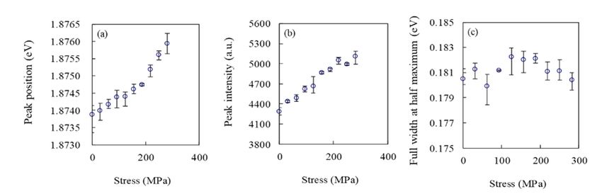
Materials 2020, 13, x FOR PEER REVIEW 3 of 9
Figure 2 depicts a representative SiO2 film specimen for tensile testing by means of conventional
MEMS fabrication techniques including photolithography, dry/wet etching, and thermal oxidation.
The specimen
Materials 2020, 13, is composed of a parallel gauge section including 200-nm-deep square concaves, 3four
4490 of 8
springs, two square chucking holes, and a frame [12–14]. An 820-nm-thick SiO2 film was coated on
the entire surface of a 4-μm-thick single crystal Si specimen by wet thermal oxidation at 1100 °C. To
checkFigure 2 depicts
the tensile test asetup
representative
for thin filmSiOstress
2 film evaluation,
specimen forwe tensile testing by means
first conducted of conventional
a quasi-static uniaxial
MEMS fabrication techniques including photolithography, dry/wet etching,
tensile test of a Si film specimen without the SiO2 film layer. The stress-strain relation was and thermal oxidation.
almost
The specimen is composed of a parallel gauge section including 200-nm-deep
linear until brittle failure, although the graph is omitted here. Young’s modulus was calculated to square concaves, four
be
springs, two square chucking holes, and a frame [12–14]. An 820-nm-thick SiO film
167 GPa, which is almost the same as the bulk value, 168.9 GPa, for Si (110) 2[16]. This indicates that was coated on the
entire
the testsurface
systemofhas a 4-µm-thick
potential as single
stresscrystal Si specimen
application by wetfor
equipment thermal
a thin oxidation at 1100 ◦ C. To check
film specimen.
the tensile
CL lighttestemitted
setup for thin
from film2 specimen
a SiO stress evaluation, we first conducted
by EB irradiation is collecteda by
quasi-static uniaxial
an ellipsoidal tensile
mirror and
test of a Si film specimen without the
led by an optical fiber to a spectrometer with SiO 2 film layer. The stress-strain relation was almost linear
a charge coupled device (CCD) detector. The excitation until
brittle
voltage, failure,
probealthough
current, andthe graph is omitted
measurement here.
time Young’s
were set to 3modulus
kV, 140 was
pA, calculated to be 167 GPa,
and 5 s, respectively, for
which is almost the same as the bulk value, 168.9 GPa, for Si (110)
stress analysis. Obtained CL spectra under various uniaxial tensile stresses were fitted[16]. This indicates that the test
using the
system has potential
Gauss/Lorentz functionas stress application
to obtain CL spectralequipment for a thin film specimen.
parameters.
Figure 2. Photograph of a SiO2 film specimen for the tensile loading test.
Figure 2. Photograph of a SiO2 film specimen for the tensile loading test.
CL light emitted from a SiO2 specimen by EB irradiation is collected by an ellipsoidal mirror and led
by an optical
3. Results andfiber to a spectrometer with a charge coupled device (CCD) detector. The excitation voltage,
Discussion
probe current, and measurement time were set to 3 kV, 140 pA, and 5 s, respectively, for stress analysis.
Figure 3 shows a representative CL spectrum of a SiO2 film without external tensile stress. The
Obtained CL spectra under various uniaxial tensile stresses were fitted using the Gauss/Lorentz
spectrum is composed of three peaks related to different types of defects in SiO2. The red spectrum is
function to obtain CL spectral parameters.
attributed to the [≡Si-O-] band of the non-bridged oxygen hole center (NBOHC), the blue one is from
theResults
3. [≡Si·] band of the trivalent Si, and the green one is from the [≡Si≡] band of the neutral oxygen
and Discussion
vacancy defect. In this study, for stress analysis, the 1.85 eV peak related to NBOHC was used due to
Figure
strongest 3 shows
peak amongathem representative
[17]. CL spectrum of a SiO2 film without external tensile stress.
The spectrum is composed of three
Figure 4 shows the relationships between peaks related toapplied
differenttensile
types of defects
stress andinCL
SiOspectral
2 . The red spectrum
parameters
is attributed
obtained from to Gauss/Lorentz
the [≡Si-O-] band of the
curve non-bridged
fitting. In all theoxygen hole center
experiments, EB was(NBOHC),
irradiated theonto
bluetheoneflat
is
from the [≡Si] band of the trivalent Si, and the green one is from the [≡Si≡]
surface of a SiO2 film specimen. In the experiment, the EB irradiation spot was unchanged, although band of the neutral oxygen
vacancy defect.
the external In this
tensile study,
stress for stress
applied was analysis,
changed in theincremental
1.85 eV peak related
steps. to NBOHC
In Figure 4a, thewas used
peak due to
position
strongest
is found to peakbe among
1.8739 them [17]. external stress. With increasing external tensile stress, the peak
eV without
Figure 4 shows the relationships
position gradually increases. When a tensile betweenstressapplied tensile
of 280 MPa wasstress andthe
applied, CLpeak
spectral parameters
position linearly
obtained from Gauss/Lorentz curve fitting. In all the experiments,
increased to 1.8760 eV. By using a least-square method for data fitting, the increment rate EB was irradiated onto the was
flat
surface of a SiO 2 film specimen. In the experiment, the EB irradiation spot
calculated to be 7.53 × 10 eV/GPa. In Figure 4b, the peak intensity also shows a trend similar to the
−3 was unchanged, although
the
peak external
position;tensile
that stress
is, theapplied
intensity was changed
linearly in incremental
increases steps. Intensile
with increasing Figurestress.
4a, theBypeak position
contrast, as
is found to be 1.8739 eV without external stress. With increasing
shown in Figure 4c, the FWHM did not show a clear correlation with tensile stress because theexternal tensile stress, the peak
position
bandwidth gradually increases.
data changed When a tensile
randomly despitestress of 280 MPa
a monotonic was applied,
change the peak
in the stress. Thoseposition linearly
CL analyses
increased to 1.8760 eV. By using a least-square method for data fitting, the increment rate was calculated
to be 7.53 × 10⁻³ eV/GPa. In Figure 4b, the peak intensity also shows a trend similar to the peak
position; that is, the intensity linearly increases with increasing tensile stress. By contrast, as shown in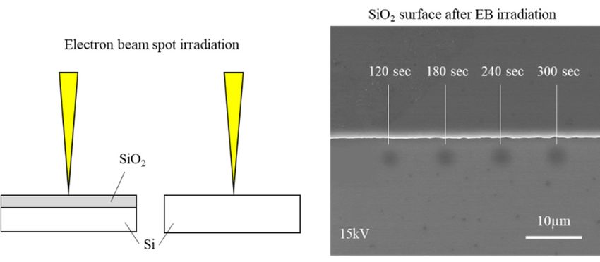
described above were conducted five times under the same condition; consequently, the trends
      obtained were consistent. Therefore, we could conclude that the peak position and intensity of the
      CL spectrum were sensitive to the external tensile stress applied.

Materials 2020, 13, 4490                                                                                                            4 of 8

Figure 4c, the FWHM did not show a clear correlation with tensile stress because the bandwidth data
changed  randomly
     Materials 2020, 13, xdespite
                          FOR PEERaREVIEW
                                    monotonic change in the stress. Those CL analyses described above
                                                                                                  4 of 9were

conducted five times under the same condition; consequently, the trends obtained were consistent.
     described above were conducted five times under the same condition; consequently, the trends
Therefore, we could conclude that the peak position and intensity of the CL spectrum were sensitive to
     obtained were consistent. Therefore, we could conclude that the peak position and intensity of the
the external   tensile stress applied.
     CL spectrum were sensitive to the external tensile stress applied.

           Figure 3. The obtained typical CL spectra from a thermally-oxidized SiO2 thin film. A typical CL
           spectrum from SiO2 (black line) and its decomposition into different contributions (red, green, and
           blue lines) by fitting Gaussian and Lorenz functions.

            Since the EB irradiation spot was unchanged irrespective of the tensile stress, the EB irradiation
      time accumulation as well as the tensile stress might have influenced the change in the CL spectral
      parameters. Therefore, we investigated the relationships between EB irradiation time and the
      parameters, as shown in Figure 5. In Figure 5a, the peak position at 5 s EB irradiation was 1.8692 eV.
      Although the irradiation time increased, the energy value at the peak position did not change that
      much. In the irradiation time range from 5 to 30 s, the difference between the maximum and
      minimum values was only 0.0007 eV. This fact suggests that the peak position was not influenced by
      Figure
      EB       3. The
          irradiation.
             Figure      obtained
                          However,
                     3. The  obtained typical
                                        two      CLCLspectra
                                               other
                                          typical      spectrafrom
                                                      parameters     aa thermally-oxidized
                                                                fromclearly                    SiO
                                                                              showed the irradiation
                                                                         thermally-oxidized  SiO    2 thin
                                                                                                 2 thin     film.
                                                                                                          time
                                                                                                        film.       A typical
                                                                                                               A influence.
                                                                                                                  typical     CL
                                                                                                                          CL The
      spectrum
      peak        fromfrom
             spectrum
            intensity,   SiO   (black
                             2 SiO
                         in Figure    5b,line)
                                   2 (black     andand
                                              line)
                                           linearly its decomposition
                                                         its decomposition
                                                      decreases            into different
                                                                             into
                                                                  with increasing         contributions
                                                                                  different contributions
                                                                                     irradiation          (red,
                                                                                                           (red,green,
                                                                                                  time, whereas   green, and
                                                                                                                         and blue
                                                                                                                    the FWHM,
      lines)
      in      by fitting
             blue
         Figure   lines)
                  5c,     Gaussian
                         by fitting
                      linearly         and Lorenz
                                     Gaussian
                                 increases       andthe
                                               with    functions.
                                                      Lorenz
                                                          time.functions.

           Since the EB irradiation spot was unchanged irrespective of the tensile stress, the EB irradiation
      time accumulation as well as the tensile stress might have influenced the change in the CL spectral
      parameters. Therefore, we investigated the relationships between EB irradiation time and the
      parameters, as shown in Figure 5. In Figure 5a, the peak position at 5 s EB irradiation was 1.8692 eV.
      Although the irradiation time increased, the energy value at the peak position did not change that
      much. In the irradiation time range from 5 to 30 s, the difference between the maximum and
      minimum values was only 0.0007 eV. This fact suggests that the peak position was not influenced by
      EB irradiation. However, two other parameters clearly showed the irradiation time influence. The
      peak intensity, in Figure 5b, linearly decreases with increasing irradiation time, whereas the FWHM,
      in Figure 5c, linearly increases with the time.

           Figure
      Figure       4. relationships
              4. The  The relationships   between
                                     between       applied
                                               applied     tensile
                                                       tensile     stress
                                                               stress andand  CL spectral
                                                                          CL spectral     parameters;
                                                                                      parameters;     (a) peak
                                                                                                  (a) peak position,
           position,
      (b) peak       (b) peak
                intensity, andintensity,
                                (c) FWHM.and (c) FWHM.

     Since the EB irradiation spot was unchanged irrespective of the tensile stress, the EB irradiation
time accumulation as well as the tensile stress might have influenced the change in the CL spectral
parameters. Therefore, we investigated the relationships between EB irradiation time and the
parameters, as shown in Figure 5. In Figure 5a, the peak position at 5 s EB irradiation was 1.8692 eV.
Although the irradiation time increased, the energy value at the peak position did not change that much.
In the irradiation time range from 5 to 30 s, the difference between the maximum and minimum values
was only 0.0007 eV. This fact suggests that the peak position was not influenced by EB irradiation.
However,Figure
            two other
                  4. The parameters      clearly showed
                          relationships between             the irradiation
                                                  applied tensile stress and CLtime  influence.
                                                                                 spectral         The(a)peak
                                                                                          parameters;    peak intensity,
in Figure position, (b) peak
           5b, linearly      intensity, with
                          decreases     and (c)increasing
                                                FWHM.      irradiation time, whereas the FWHM, in Figure 5c,
linearly increases with the time.
     From the investigation shown in Figures 4 and 5, the peak position of the CL spectrum is a strong
candidate as the representative parameter for SiO2 stress analysis. This is because the parameter was
sensitive to only tensile stress, and it was insensitive to the EB irradiation time. The intensity and
FWHM were obviously sensitive to the irradiation time. This experimental fact implies that some
physical damage was introduced into the SiO2 film by EB irradiation accumulation. To investigate
how the damage was introduced, Raman spectroscopy and TEM observations around EB irradiation
points were conducted. As shown in Figure 6, EB spots were irradiated using an SEM onto Si and SiO2
film surfaces at 15 kV for 120, 180, 240, and 300 s. Each spot interval was set to be 10 µm. As shown
shown in the SEM image, the irradiated spots formed on the SiO2 film presented a mottled pattern
due to contamination or some damage.
Figure 7 shows representative Raman spectroscopic line scanning results showing (a) the Raman
peak shift, (b) peak intensity, and (c) FWHM. The analysis was conducted using a commercial Raman
spectroscope
Materials 2020, 13,(HORIBA
4490 Jobin Yvon, LabRAM HR-800, Kyoto, Japan). The sample stage of5 the of 8
microscope was driven using a piezoelectric actuator in 1 μm steps. The black and gray plots are
indicative of the analysis result on the SiO2 and Si surfaces, respectively. In Figure 7a, the peak
in the SEM
position of image, the irradiated
each Raman spots
spectrum formed
obtained at on theposition
each SiO2 filmonpresented a mottled
the Si surface patternroughly
remained due to
Materials 2020, 13, x FOR PEER REVIEW 5 of 9
contamination or some damage.
constant, ranging from 518.96 to 519.10 cm , which are close to the typical value for Si, 520 cm−1.
−1
However, in the case of the SiO2 surface, a different trend was obtained. For example, for the EB
irradiated point for 120 s, the peak position shifted by around 0.1 cm−1 compared with the non-
irradiated point. The amount of the peak shift monotonically increased to around 0.2 cm−1 with an
increase in the irradiation time up to 300 s. Raman peak shift is well known to be related to stress
applied to an analyzed point. The peak shift to the high cm−1 direction indicates that compressive
stress was applied. As shown in Figure 7b,c, no wavy distribution occurred in the peak intensity and
FWHM on both SiO2 and Si surfaces, indicating that there was no influence of EB irradiation on these
parameters. Since the Raman peak shift is strongly influenced by the crystal structure of a material
[18], the phenomenon, indicating Raman stress change around EB irradiation spots, was possibly
caused by a5.structural
Figure changebetween
Therelationships
relationships inside EB
theirradiation
SiO2 filmtime
or someCLkind
andCL of damage
spectral at the
parameters; SiO2position,
(a)peak
peak /Si interface
Figure 5. The between EB irradiation time and spectral parameters; (a) position,
caused by
(b) peak the irradiation.
peak intensity,
intensity, and Based on the above results, however, no possibility of some SiO2/Si
(b) and (c)
(c) FWHM.
FWHM.
interface damage is expected.
From the investigation shown in Figures 4 and 5, the peak position of the CL spectrum is a strong
candidate as the representative parameter for SiO2 stress analysis. This is because the parameter was
sensitive to only tensile stress, and it was insensitive to the EB irradiation time. The intensity and
FWHM were obviously sensitive to the irradiation time. This experimental fact implies that some
physical damage was introduced into the SiO2 film by EB irradiation accumulation. To investigate
how the damage was introduced, Raman spectroscopy and TEM observations around EB irradiation
points were conducted. As shown in Figure 6, EB spots were irradiated using an SEM onto Si and
SiO2 film surfaces at 15 kV for 120, 180, 240, and 300 s. Each spot interval was set to be 10 μm. As
shown in the SEM image, the irradiated spots formed on the SiO2 film presented a mottled pattern
due to contamination
Figure 6. Schematic orofsome damage. along with the
irradiation
EB irradiation the SEM
SEM imageimage of of the
the SiO
SiO22 surface.
surface. The four-circle
Figure
pattern7can shows representative
be observed on the Raman
SiO
on the SiO2 2 surfacespectroscopic
after EB spot line scanning
irradiation. results showing (a) the Raman
peak shift, (b) peak intensity, and (c) FWHM. The analysis was conducted using a commercial Raman
spectroscope (HORIBA
Figure 7 shows Jobin Yvon,
representative LabRAM
Raman HR-800,line
spectroscopic Kyoto,
scanningJapan). Theshowing
results sample (a) stage of the
the Raman
microscope
peak shift, (b) waspeakdriven using a and
intensity, piezoelectric
(c) FWHM. actuator in 1 μm was
The analysis steps. The blackusing
conducted and gray plots are
a commercial
indicative of the analysis
Raman spectroscope (HORIBA resultJobin
on theYvon,SiOLabRAM
2 and Si HR-800,
surfaces,Kyoto, respectively.
Japan). In TheFigure
sample7a, the of
stage peak
the
position
microscopeof each Raman using
was driven spectrum obtained atactuator
a piezoelectric each position
in 1 µmon the Si
steps. Thesurface
black remained
and gray plotsroughly are
constant,
indicativeranging from 518.96
of the analysis result onto 519.10
the SiOcm −1, which
2 and are close
Si surfaces, to the typical
respectively. In Figure value for peak
7a, the Si, 520 cm−1.
position
However, in the
of each Raman case of obtained
spectrum the SiO2 at surface, a different
each position on thetrend was obtained.
Si surface For example,
remained roughly constant,for ranging
the EB
irradiated
from 518.96point for 120
to 519.10 −1
cm s,, the
whichpeak areposition
close to theshifted by value
typical around for0.1 cm cm
Si, 520 −1 −1
compared
. However, withinthethenon-
case
irradiated
of the SiO2point.
surface,Thea different
amount of the was
trend peakobtained.
shift monotonically
For example, increased
for the EB to irradiated
around 0.2point with
cm−1 for 120ans,
increase
the peakin the irradiation
position shifted by time up to0.1
around 300cm s.−1Raman
comparedpeakwith shifttheis well known to be
non-irradiated related
point. Theto stress
amount
applied to an
of the peak analyzed
shift point. The
monotonically peak shift
increased to the 0.2
to around high −1
cmcm with
−1 direction indicates
an increase in thethat compressive
irradiation time
stress
up to was
300 applied.
s. Raman Aspeakshown in Figure
shift is well 7b,c,
known no wavy distribution
to be related to stressoccurred
applied in the
to peak intensitypoint.
an analyzed and
FWHM
The peak onshift
bothto SiO
the2 and
highSicm −1
surfaces, indicating
direction that there
indicates was no influence
that compressive stressofwasEB irradiation
applied. As onshown
these
parameters.
in Figure 7b,c, Since the Raman
no wavy peak shift
distribution is strongly
occurred in theinfluenced
peak intensity by the and crystal
FWHM structure
on bothofSiO a material
2 and Si
[18], the phenomenon,
surfaces, indicating that indicating
there was no Raman stress
influence of change aroundonEB
EB irradiation irradiation
these parameters. spots, wasthe
Since possibly
Raman
caused by isa strongly
peak shift structural change inside
influenced by thethe SiO2structure
crystal film or some kind of [18],
of a material damage at the SiO2/Siindicating
the phenomenon, interface
caused
Raman bystressthechange
irradiation.
aroundBased on the above
EB irradiation spots,results,
was possiblyhowever, caused no bypossibility
a structural of change
some SiO 2/Si
inside
interface damage
the SiO2 film kind of damage at the SiO2 /Si interface caused by the irradiation. Based on the
is expected.
or some
above results, however, no possibility of some SiO2 /Si interface damage is expected.
Figure 8 shows TEM images of SiO2 thin films after EB irradiation. All specimens for TEM
observation were prepared using an ion slicer (JEOL Ltd., EM-09100IS, Tokyo, Japan). After the
preparation, the surface was irradiated with EB under the following conditions: 3 kV, 140 pA, and 5 s.
For the observation, a TEM (FEI Company, Tecnai 20 ST, Hillsboro, OR, USA) was used, and the
excitation voltage and emission current were set to 200 kV and 5.48 µA, respectively. Before EB
irradiation, a typical amorphous structure was observed, although some low-contrast small dots were
Figure 6. Schematic of EB irradiation along with the SEM image of the SiO2 surface. The four-circle
pattern can be observed on the SiO2 surface after EB spot irradiation.Materials 2020, 13, 4490 6 of 8
detected. After 5 s irradiation, several tens of dots shown as black mottles were clearly observed,
with a diameter of around 2 nm. In spite of the very short-duration irradiation, those small dots were
produced in the SiO2 film. After irradiation for 1000 s, numerous dots with approximately 3~5 nm
diameter were obtained in the entire TEM image, which indicates that the quantum dots grew by
successive EB irradiation. In the magnified photograph, the dot consists of a lattice pattern with
approximately 0.2 nm intervals, which is in close agreement with the lattice spacing in the Si (220)
plane [19]. This strongly suggests that EB-irradiation-induced nano-dots are probably nanocrystals
made of single crystal Si. The generation of Si nanocrystals in SiO2 would be caused by Si-O network
disconnection and oxygen desorption [20–22]. Because the nanocrystals were stressed by the SiO2 film,
Raman stress distribution was probably changed around EB irradiation spots [23]. Also, a change in
the CL spectrum was influenced by not only the SiO2 film structure change but also stress from SiO2
caused to Si nanocrystals. However, the mechanisms of changing Raman stress after EB irradiation,
shown in Figure 7a, and changing CL intensity and FWHM shown in Figure 5b,c), should not be
concluded until further experiments have been performed. Even though the EB irradiation time
was just 5 s, which is the same irradiation energy (1.8 × 10⁻⁴ J/m2 ) as that in the CL stress analysis
experiment, Si nanocrystals were generated. To measure the stress in SiO2 film using CL spectroscopy
without any2020,
Materials damage, anPEER
13, x FOR EB REVIEW
irradiation condition without Si nanocrystal formation must be specified.
6 of 9
Figure 7. The7.influence
Figure of EB irradiation
The influence on the SiO
of EB irradiation andSiO
on 2the Si 2surface
and Siobserved with Raman
surface observed withspectroscopy;
Raman
(a) peak shift, (b) peak
spectroscopy; intensity,
(a) peak and
shift, (b) (c)intensity,
peak FWHM.and (c) FWHM.
Materials 2020, 13, x FOR PEER REVIEW 7 of 9
Figure 8 shows TEM images of SiO2 thin films after EB irradiation. All specimens for TEM
observation were prepared using an ion slicer (JEOL Ltd., EM-09100IS, Tokyo, Japan). After the
preparation, the surface was irradiated with EB under the following conditions: 3 kV, 140 pA, and 5
s. For the observation, a TEM (FEI Company, Tecnai 20 ST, Hillsboro, OR, USA) was used, and the
excitation voltage and emission current were set to 200 kV and 5.48 μA, respectively. Before EB
irradiation, a typical amorphous structure was observed, although some low-contrast small dots were
detected. After 5 s irradiation, several tens of dots shown as black mottles were clearly observed, with
a diameter of around 2 nm. In spite of the very short-duration irradiation, those small dots were
produced in the SiO2 film. After irradiation for 1000 s, numerous dots with approximately 3~5 nm
diameter were obtained in the entire TEM image, which indicates that the quantum dots grew by
successive EB irradiation. In the magnified photograph, the dot consists of a lattice pattern with
approximately 0.2 nm intervals, which is in close agreement with the lattice spacing in the Si (220)
plane [19]. This strongly suggests that EB-irradiation-induced nano-dots are probably nanocrystals
made of single crystal Si. The generation of Si nanocrystals in SiO2 would be caused by Si-O network
disconnection and oxygen desorption [20–22]. Because the nanocrystals were stressed by the SiO2
film, Raman stress distribution was probably changed around EB irradiation spots [23]. Also, a
change in the CL spectrum was influenced by not only the SiO2 film structure change but also stress
from SiO2 caused to Si nanocrystals. However, the mechanisms of changing Raman stress after EB
irradiation, shown in Figure 7a, and changing CL intensity and FWHM shown in Figure 5b,c), should
not be concluded until further experiments have been performed. Even though the EB irradiation
time was just 5 s, which is the same irradiation energy (1.8 × 10⁻⁴ J/m2) as that in the CL stress analysis
Figure 8. TEM images of SiO2 films after EB irradiation for (a) 0 s, (b) 5 s, (c) 1000 s, and (d) Enlarged
Figure 8.
experiment,TEM Siofimages of SiO2 films
nanocrystals after EB irradiation
To measurefor the(a) 0 s, (b) 5 s,2 (c) 1000 s, and (d) Enlarged
view an Si nanodot. were generated. stress in SiO film using CL spectroscopy
view of an Si nanodot.
without any damage, an EB irradiation condition without Si nanocrystal formation must be specified.
4. Conclusions
We investigated the relationships between CL spectra of SiO2 film and external tensile stresses
applied, for non-destructive stress analysis with a CL spectroscope. It was possible to estimate the
stress on the SiO2 film directly from the CL peak shift because the peak position of the CL spectra
linearly increased with increasing applied stress at a constant rate of 7.53 × 10⁻³ eV/GPa. However,
Raman spectroscopy and TEM analysis suggested that Si nanocrystals were formed at the EBMaterials 2020, 13, 4490 7 of 8
4. Conclusions
We investigated the relationships between CL spectra of SiO2 film and external tensile stresses
applied, for non-destructive stress analysis with a CL spectroscope. It was possible to estimate the
stress on the SiO2 film directly from the CL peak shift because the peak position of the CL spectra
linearly increased with increasing applied stress at a constant rate of 7.53 × 10⁻³ eV/GPa. However,
Raman spectroscopy and TEM analysis suggested that Si nanocrystals were formed at the EB irradiation
point on the SiO2 film, which indicated that the SiO2 film suffered from damage by EB irradiation.
The Si nanocrystals generated affected the CL intensity and FWHM. For current CL stress analysis of
SiO2 film, CL measurement for the shortest time would be necessary to limit damage.
In future, for realization of non-destructive CL stress analysis, it is required to quantitatively
and experimentally understand the amount of Si nanocrystal formation in SiO2 film caused by EB
irradiation, and then to establish the CL analysis condition to avoid the formation of Si nanocrystals.
Moreover, considering CL stress analysis practical use in semiconductor industry, it is also important
to consider the possibility of changes in CL spectra with elevated temperature.
Author Contributions: Conceptualization, K.N. and N.N.; methodology, N.Y.; investigation, S.K.
(Shingo Kammmachi), Y.G., N.G., N.Y., S.K. (Shigeru Kakinuma), N.N., and S.I.; writing—original draft preparation,
S.K. (Shingo Kammmachi); writing—review and editing, T.N.; supervision, T.N.; project administration, T.N.
All authors have read and agreed to the published version of the manuscript.
Funding: This research received no external funding.
Conflicts of Interest: The authors declare no conflict of interest.
References
1. Naka, N.; Kashiwagi, S.; Nagai, Y.; Namazu, T.; Inoue, S.; Ohtsuki, K. Raman Spectroscopic Study for
Determining Stress Component in Single Crystal Silicon Microstructure using Multivariate Analysis.
In Proceedings of the 2007 International Conference on Solid State Devices and Materials, Tsukuba, Tokyo,
18–21 September 2007; pp. 392–393. [CrossRef]
2. Walraven, J.A. Future challenges for mems failure analysis. In Proceedings of the International Test
Conference, Charlotte, NC, USA, 30 September–2 October 2003; Volume 1, pp. 850–855.
3. Komatsubara, M.; Namazu, T.; Naka, N.; Kashiwagi, S.; Ohtsuki, K.; Inoue, S. Non-Destructive Quantitative
Measurement Method for Normal and Shear Stresses on Single-Crystalline Silicon Structures for Reliability of
Silicon-MEMS. In Proceedings of the 2009 IEEE 22nd International Conference on Micro Electro Mechanical
Systems, Sorrento, Italy, 25–29 January 2009; pp. 659–662.
4. De Wolf, I. Stress measurements in Si microelectronics devices using Raman spectroscopy. J. Raman Spectrosc.
1999, 30, 877–883. [CrossRef]
5. Xu, Z.; He, Z.; Song, Y.; Fu, X.; Rommel, M.; Luo, X.; Hartmaier, A.; Zhang, J.; Fang, F. Application of Raman
Spectroscopy Characterization in Micro/Nano-Machining. Micromachines 2018, 9, 361. [CrossRef] [PubMed]
6. Glunz, S.W.; Feldmann, F. SiO2 Surface passivation layers—A key technology for silicon solar cells.
Solar Energy Mater. Solar Cells 2018, 158, 260–269. [CrossRef]
7. Paskov, P.; Schifano, R.; Monemar, B.; Paskova, T.; Figge, S.; Hommel, D. Emission properties of a-plane GaN
grown by metal-organic chemical-vapor deposition. J. Appl. Phys. 2005, 98, 93519. [CrossRef]
8. Imura, M.; Honshio, A.; Miyake, Y.; Nakano, K.; Tsuchiya, N.; Tsuda, M.; Okadome, Y.; Balakrishnan, K.;
Iwaya, M.; Kamiyama, S.; et al. Microstructure of Nitrides Grown on Inclined c-Plane Aapphire and SiC
Substrate. Phys. Rev. B 2006, 491, 376–377.
9. Namazu, T.; Yamashita, N.; Kakinuma, S.; Nishikata, K.; Naka, N.; Matsumoto, K.; Inoue, S.
In-situ cathodoluminescence spectroscopy of silicon oxide thin film under uniaxial tensile loading.
J. Nanosci. Nanotechnol. 2011, 11, 2861–2866. [CrossRef] [PubMed]
10. Leto, A.; Porporati, A.A.; Zhu, W.; Green, M.; Pezzotti, G. High-resolution stress assessments of
interconnect/dielectric electronic patterns using optically active point defects of silica glass as a stress
sensor. J. Appl. Phys. 2007, 101, 93514. [CrossRef]Materials 2020, 13, 4490 8 of 8
11. Kodera, M.; Iguchi, T.; Tsuchiya, N.; Tamura, M.; Kakinuma, S.; Naka, N.; Kashiwagi, S. Nano-Scale
Stress Field Evaluation with Shallow Trench Isolation Structure Assessed by Cathodoluminescence, Raman
Spectroscopy, and Finite Element Method Analyses. Ext. Abst. SSDM 2007, 934–935. [CrossRef]
12. Namazu, T.; Nagai, Y.; Naka, N.; Araki, N.; Inoue, S. Design and Development of a Biaxial Tensile Test Device
for a Thin Film Specimen. J. Eng. Mater. Technol. 2011, 134, 011009. [CrossRef]
13. Fujii, M.; Namazu, T.; Fujii, H.; Masunishi, K.; Tomizawa, Y.; Inoue, S. Quasi-Static and Dynamic Mechanical
Properties of Al-Si-Cu Structural Films in Uniaxial Tension. J. Vac. Sci. Technol. B 2012, 30, 031804. [CrossRef]
14. Namazu, T.; Fujii, M.; Fujii, H.; Masunishi, K.; Tomizawa, Y.; Inoue, S. Thermal Annealing
Effect on Elastic-Plastic Behavior of Al-Si-Cu Structural Films under Uniaxial and Biaxial Tension.
J. Microelectromech. Syst. 2013, 22, 1414. [CrossRef]
15. Namazu, T.; Kuwahara, K.; Fujii, M.; Kanetsuki, S.; Miyake, S.; Inoue, S. Mechanical reliability of
reactively-formed NiAl alloys as a structural material. Sens. Mater. 2016, 28, 141.
16. Brantley, W.A. Calculated elastic constants for stress problems associated with semiconductor devices.
J. Appl. Phys. 1973, 44, 534. [CrossRef]
17. Skuja, L. Optically active oxygen-deficiency-related centers in amorphous silicon dioxide.
J. Non-Crystalline Solids 1998, 239, 16–48. [CrossRef]
18. Katoda, T.; Nakamura, T. Characterization of Semiconductors by Laser-Raman Spectroscopy. Jpn. Soc.
Appl. Phys. 1981, 50, 69–76.
19. Nakayama, K.; Fujii, K. Absolute determination of lattice spacing and the Avogadro constant. Jpn. Soc.
Appl. Phys. 1993, 62, 245–252.
20. Chen, G.S.; Boothroyd, C.B.; Humphreys, C.J. Electron-beam-induced damage in amorphous SiO2 and the
direct fabrication of silicon nanostructures. Philos. Mag. A 1998, 78, 491–506. [CrossRef]
21. Yu, K.; Xu, T.; Wu, X.; Wang, W.; Zhang, H.; Zhang, Q.; Tang, L.; Sun, L. In Situ Observation of Crystalline
Silicon Growth from SiO2 at Atomic Scale. Research 2019. [CrossRef]
22. Dey, P.P.; Khare, A. Fabrication of photoluminescent nc-Si:SiO2 thin films prepared by PLD. Phys. Chem.
Chem. Phys. 2017, 19, 21436–21445. [CrossRef]
23. Nikitin, T.; Khriachtchev, L. Optical and Structural Properties of Si Nanocrystals in SiO2 Films. Nanomaterials
2015, 5, 614–655. [CrossRef]
© 2020 by the authors. Licensee MDPI, Basel, Switzerland. This article is an open access
article distributed under the terms and conditions of the Creative Commons Attribution
(CC BY) license (http://creativecommons.org/licenses/by/4.0/).You can also read