Lead-free Electronics Reliability - An Update - Andrew D. Kostic, Ph. D. The Aerospace Corporation
←
→
Page content transcription
If your browser does not render page correctly, please read the page content below

Lead-free Electronics Reliability - An Update

Andrew D. Kostic, Ph. D.
The Aerospace Corporation

GEOINT DEVELOPMENT OFFICE
August 2011

© The Aerospace Corporation 2011

Lead (Pb) – Some Background

•   Lead (Pb) has been used by humans since at least 6500 BC
    – Pb solder use dates back to 3800 BC when it was used to produce
      ornaments and jewelry
•   Harmful effects of excess Pb on the human body are well documented
     –   Pb gets into the body only through inhalation or ingestion
     –   Acts as a neurotoxin, inhibits hemoglobin production, effects brain
         development
     –   Children are more susceptible than adults
•   Dramatic reduction in blood Pb levels since 1975 due mainly use of
    Pb-free gasoline
     –   78% reduction documented in 1994 by EPA
     –   Elimination of Pb from paints gave additional benefit

2
Lead Consumption
•   World wide consumption of refined Pb decreased slightly to 8.63 metric
    tons in 2009 from 8.65 metric tons in 2008
     –   The first annual decline in global Pb consumption since 2001
•   The leading refined-Pb-consuming countries in 2009 were:
     –   China 45%
     –   United States 16%
     –   Germany 4%
     –   Republic of Korea 3%.
•   Consumption of refined Pb in the U.S. decreased by about 11% in 2009
                   Application                    2009 U.S. Consumption
                 Metal Products                                  5.8%
                Electronic Solder                                0.5%
                Storage Batteries                               88.3%

                 1) International Lead and Zinc Study Group (2010c, p. 8–9) (ILZSG),
                 2) Data from USGS statistics
3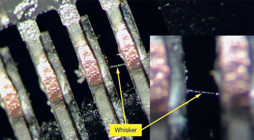
Pb in the Electronics Industry

•   Electronic component terminations have been electroplated and
    soldered to circuit boards with tin/lead (Sn/Pb) solder for many decades
•   The entire electronics manufacturing process has been developed
    around the mechanical properties and soldering temperature of Sn/Pb
    –   Component packaging
    –   PCB material
    –   Design rules
    –   Thermal management

4
The Concern Regarding Pb in Electronics
•   Apprehension about Pb from waste electronics entering the ecosystem
    –   Pb in solder and platings might leach away and get into ground water
•   “Green” movement in the European Union (EU) looked for ways to
    reduce Pb in landfills
•   Consumer electronics account for 40% of Pb in landfills
•   Recycling efficiency of Pb in consumer electronics is 5%

5
The Precautionary Principle
Ready, Fire, Aim!

•   Precautionary Principle states:
    – “When an activity raises threats of harm to human health or the
      environment, precautionary measures should be taken even if some
      cause-and-effect relationships are not fully established scientifically.”
•   Used as the basis for enacting environmental legislation in the EU
    and other countries around the world

6
What is RoHS?
    • Fears over imagined harm from Pb used in consumer electronics
        resulted in legislative action in the Europe Union (EU)
    •   The EU issued the Restrictions on Hazardous Substances (RoHS)
        directive in 2003
        –   Prohibits certain substances in specific categories of electronic
            equipment sold in EU member nations
             • Prohibited materials are lead, mercury, cadmium, hexavalent
               chromium, polybrominated biphenyls (PBB) or polybrominated
               diphenyl ethers (PBDE)
             • Lead (Pb) not allowed in concentrations of greater than 0.1% by
               weight in component termination finishes and solder
        –   Supporting laws took effect on July 1, 2006
    •   RoHS fundamentally altered the electronics industry worldwide!

7
RoHS Exemptions
•   RoHS exemptions are regularly reviewed and changed by the EU
     – Fewer exemptions are being granted
•   Military and aeronautic/aerospace equipment are currently considered
    excluded/exempt/out of scope in guidance documents
•   Automotive electronics must be RoHS compliant in the EU by 2016
•   Medical electronics must be RoHS compliant in the EU by 2014
     –   Defibrillators exempt until 2021

8
Global Environmental Initiatives

9

Transition Costs
     •   In 2005, Intel made the following statements
           – “Intel's ($34.2B annual revenue) efforts to remove lead from its chips
              have so far cost the company more than $100 million and there is no
              clear end in sight to the project's mounting costs”
          –   “the company hopes to be completely lead-free within five years”
                • http://www.infoworld.com/article/05/03/16/HNleadfreemove_1.html

     •   In 2011, Intel is still not completely Pb-free although some of their
         product lines have achieved that status

10
Pb Reductions Achieved
• A huge (~ $14B annual revenue) semiconductor manufacturer
estimated the annual worldwide Pb reduction per 1,000,000,000
integrated circuits was only equivalent to ~100 automobile batteries
– This is less than 0.05% of car batteries that are not recycled yearly
11Pb Entering the Environment – Groundwater Pollution
• “In the environment, inorganic lead will mainly be particulate bound with
relatively low mobility and bioavailability. Under most circumstances, humic
substances will immobilize the lead. However, as the alkalinity and pH
decreases the mobility of lead increases.”
– “Phasing out lead in solders” Ulrika Kindesjö, 2001
• “Natural weathering processes usually turn metallic lead and its
compounds into compounds which are relatively stable and insoluble.”
– "LEAD: the facts" is an independent report on lead and its industry
prepared by Imperial College Consultants Ltd (London, UK) and was
published in December 2001.
12Pb Entering the Environment – Groundwater Pollution
• “Lead does not break down in the environment. Once lead falls on
to soil, it usually sticks to the soil particles.”
• Ohio Department of Health 08/10/09
– “Lead – Answers to Frequently Asked Health Questions”
• 148 year long continuing study in Brandy Station, Virginia by the
author confirms Pb does not leach away
– Land has been farmed continuously
.577 Caliber French Triangle Cavity Bullet
“Minie Ball”
Reprinted with permission of Andrew D. Kostic
13Pb Entering the Environment – Recycling Impact
• Concern about recycling electronics in third world countries over
open fires
– May create Pb vapor that would be inhaled causing Pb poisoning
• Pb boils at 1,740 C
• Typical open fire temperature is approximately 1,000 C
– Vapor pressure of Pb is negligible at that temperature
• Little/no possibility of Pb vapor inhalation
• Same reason why Sn/Pb soldering personnel do not have elevated
blood Pb levels
1415
Lead Poisoning from Electronics
• There is no evidence that Pb used in electronics manufacturing
and products does any harm to humans or the environment
– Electronics industry consumes approximately 0.5% of world’s Pb
– No mechanism exists for transfer of Pb to blood through direct contact or
proximity to Pb in electronics
– No evidence of any elevated Pb levels in blood of soldering personnel
• Lead-acid batteries account for over 80% of Pb consumed
– Batteries are exempt from all RoHS legislation
15Environmental Impact of Pb-free Replacements
• Current alternatives are worse for the environment
• Study by IKP University of Stuttgart Department Life Cycle Engineering
– http://leadfree.ipc.org/files/RoHS_15.pdf
• Boundary Conditions of the Study:
– The calculations are “cradle to gate” analysis, that means from extraction of
the raw materials up to the finished product, including all pre-chains like
energy supply or production of auxiliaries.
– The life cycle phase “End of The Life”(recycling/deposition/incineration) is
not considered, as there are no reliable data available today on the
respective impacts (especially on landfills). In case considerable quantities
of heavy metals are emitted from those landfills, this could have significant
influence to the overall results.
16Comparison of Human Toxicity Potential
(Extraction to Finished Product)
Source: Neil Warburg, IKP University of Stuttgart, Life-Cycle Study
17Comparison of Acidification Potential
(Extraction to Finished Product)
Source: Neil Warburg, IKP University of Stuttgart, Life-Cycle Study
18Comparison of Global Warming Potential
(Extraction to Finished Product)
Source: Neil Warburg, IKP University of Stuttgart, Life-Cycle Study
19Comparison of Primary Energy Use
(Extraction to Finished Product)
Source: Neil Warburg, IKP University of Stuttgart, Life-Cycle Study
20US Federal and State Legislation
• No Federal restriction on Pb in electronics…yet
• California State-level legislation
– Regulations effective January 1, 2007
• Forbid sale of devices containing materials prohibited by EU RoHS but
with narrow focus: CRTs, LCDs, Plasma Displays, etc (>4” screen)
• Other states have “environmental” legislation similar to the EU
including New Jersey
21Lack of Technical Guidance
• DoD
– No position
• Federal Aviation Agency (FAA)
– No official position
• NASA
– Prohibits pure tin as a finish and often requires 3% lead
• European Space Agency (ESA)
– Tin/lead required solder for assembly
2223 Cartoon by Nick D Kim, strange-matter.net. Used by permission
Suppliers Have Converted to Pb-free Products
 • The suppliers are making the vast majority of their products for
     commercial applications
     –   Reaction to the RoHS restrictions
     –   Marketing decision to provide “green” products
                                 COMPONENT
                                  FINISHES

24
Suppliers Have Converted to Pb-free Products
• Most aerospace/military parts are “dual-use” (both commercial and
mil/aero) so many parts are only available as Pb-free
– Not viable to keep a Sn/Pb manufacturing process for small market
– Military/aerospace is less than 1% of the market
• Many different aspects of products have changed
– Termination finishes
– PWB finishes COMPONENT
FINISHES
– Solder
– Layout
– Process flow
25Pb-free - Not “If” but “When” 26
Product Availability
• Some component suppliers continue to offer both RoHS-compliant
     versions and heritage Sn/Pb parts
      –   Number of suppliers offering Sn/Pb is decreasing
•    Contract assembly houses have also moved to Pb-free
      –   Some capacity remains for Sn/Pb assembly but is limited
•    Industry trends for heritage Sn/Pb parts
      –   Lack of availability (DMS)
      –   Long lead times
      –   Price increases
      –   Increasing risk of counterfeit parts

27
No Drop-in Replacement for Sn/Pb
• There are still no “drop-in replacements” for Sn/Pb solder or plating
• Industry still has not standardized on a replacement for Sn/Pb solder
– Mechanical characteristics of solders have wide variations
– Different alloys have different reflow temperatures
– Alloys may not interact well
• Some alloys covered by patents or copyrights
– Finished solder joint compositions covered too!
28Trends in Pb-free Solders
• In 2005 the “answer” was SAC305
– Sn(96.5%)Ag(3%)Cu(0.5%)
– It did not live up to expectations
• More alloys are being used for specific applications as limitations of
existing alloys are discovered
– SAC105
– SAC405
– Sn100C (Nihon Superior)
– Sn99.3Cu0.7 with cobalt
– Sn/Bi
– K100LD tin/copper/nickel+bismuth (Kester)
– CASTIN (Aim Solder)
– Tin/Copper (Sn/Cu)
– Tin/Copper/Nickel (Sn/Cu/Ni)
– Tin/Bismuth (Sn/Bi)
– Tin/Bismuth/Zinc (Sn/Bi/Zn)
– Tin/Silver/Bismuth (Sn/Ag/Bi)
29Component Termination Finishes
• Finishes containing Pb have basically been discontinued
– Well over 90% are Pb-free
– Many suppliers consider Sn/Pb special orders
• Pure Sn is the usual choice for termination finish
• Nickel/Palladium/Gold (Ni/Pd/Au) is a common Pb-free alternative to Sn
– Additional cost
30Some Pb-free Component Finishes
• Gold (Au)
• Tin (Sn)
• Matte Tin (Sn)
• Nickel/Palladium/Gold (Ni/Pd/Au)
• SAC105 (Sn/Ag/Cu)
• SAC305 (Sn/Ag/Cu)
• SAC405 (Sn/Ag/Cu)
• Tin/Copper (Sn/Cu)
• Tin/Copper/Nickel (Sn/Cu/Ni)
• Tin/Bismuth (Sn/Bi)
• Tin/Bismuth/Zinc (Sn/Bi/Zn)
• Tin/Silver/Bismuth (Sn/Ag/Bi)
31Impacts of Change to Pb-free Solders and Finishes
• Inability of users to know what material they are getting
• Identification methods varies
– New part numbers
– Marking on packaging
– Date of manufacture
– Marked on part
• Cannot visually differentiate between Sn/Pb and Pb-free Sn
– Lot sampling is mandatory
– Energy dispersive x-ray analysis (EDX) and x-ray fluorescence (XRF) are
common inspection tools
• Typically +/- 1% absolute accuracy in measuring Pb in a Sn matrix
32Impacts of Change to Pb-free Solders and Finishes
• Visual inspection criteria for solder joints are different
– Rejected Sn/Pb joint would typically be acceptable in a Pb-free solders
– Significant operator retraining required
• Mixing technologies during assembly, repair, or upgrade
– Difficulty in tracking parts with differing finishes
– Different assembly techniques required
33Pb-free Solder Assembly and Inspection Issues
PWB Laminate Stress
Inspection
Components
Wetting and
Storage Life
Higher Assembly Temperature
~ 35°C
higher
Improper Reflow
34Impacts of Change to Pb-free Solders and Finishes
• Even materials that are not specifically called out in RoHS have
changed in response to Pb-free soldering
– Laminates, fluxes …
• Use of no-clean fluxes results in greater likelihood of conductive flux
residues on board after assembly
• Emergence of new/unfamiliar failure modes
35Impacts of Change to Pb-free Solders and Finishes
• Process and reliability improvements have been/are being developed
for consumer electronics environments
– Not optimized for high reliability, severe stress, long life applications
• Different solders may be needed for each different application
depending on operating conditions and environment
– Temperature, thermal cycle, vibration, shock …
36Rework and Repair Are Major Concerns
• Hardware will be received back for repair
– Only available replacement parts in many cases will be Pb-free
– What records will identify termination finish or solder alloy used?
• Cannot mix Sn/Pb and Pb-free solder on some components (e.g.,
BGAs) without risk to reliability
– Level of risk is still the subject of numerous studies
“Backward Compatibility” Problematic
37Pb-free Reliability Issues
Increased solder voiding
Microvoiding
Less Reliability @ High Temps and Vibration
Mixed Technology
Sn/Pb paste/SAC ball Sn/Pb paste/SAC ball
205°C peak reflow 214°C peak reflow
25% Decrease in
Reliability
Sn / (3-4 wt%) Ag / (0.5-0.7 wt%) Cu
Pb
crack diffusion
Pb diffusion
38Solderability
• Lead free solders have decreased wetting ability
– Lead free surface finishes on components and boards will also decrease the
amount of wetting
– Longer exposure at increased temperatures will assist wetting at the risk of
thermal damage
• Lead-free component finishes and solders typically require higher
soldering temperatures which will affect
– Cost
– Reliability
– Rework
• Re-qualification required for components used in a lead-free assembly
processes
39 39Pb-free Solder – Durability
• Field to lab correlation has not been established for Pb-free
– Especially in high stress long life applications
• Pb-free (SAC) interconnects less reliable at
– Higher temperatures
– Vibration
– Shock
• Not an issue for consumer products because of low stress levels
– Low stress: Pb-free is better
– High stress: SnPb is better
40Pb-free Tin Reliability Issues Tin Whiskers 41
What are Tin Whiskers?
 •   Tin whiskers are spontaneous hair-like growths from surfaces that use
     Pb-free tin (Sn) as a final finish
      –   Electrically conductive
      –   May grow in hours, days, weeks, or years
      –   Pb-free tin-plated electronic & mechanical parts can grow whiskers
           • Nuts, Bolts …

                     Courtesy: NASA Electronic Parts and Packaging (NEPP) Program
42
Tin Whisker Background
• Tin whiskers were first reported by Bell Labs around 1947
• Growth inception and rate varies widely
– Can start growing after years of dormancy or in a few hours
– Whiskers can start growing, stop, and then resume growing
• Whisker shapes and forms vary considerably
• Lengths range from few microns to over 20 millimeters
– 23 millimeters is the current record holder
• Up to 200 whiskers per square millimeter have been observed
• Whiskers can grow through thin conformal coatings
http://www.calce.umd.edu/lead-free/
http://nepp.nasa.gov/whisker/
43Tin Whisker Background
• Whisker growth mechanism(s) still not known after 60+ years of study
– Conflicting evidence
• No effective tests to determine the whisker propensity of platings
• No single mitigation technique provides effective protection against
whisker formation except the addition of 3% or more of Pb by weight
• No reliability models exist that can quantify impact of tin whiskers
• Whiskers are extremely difficult to detect
– Many “No Defect Found/Could Not Duplicate/No Trouble Found”
faults may be due to tin whiskers
44What Causes Tin Whiskers?
Plating Chemistry Substrate
Pure Sn Most Prone
Material (Brass, Cu, Alloy 42, Steel, etc.)
Some Alloys (Sn-Cu, Sn-Bi, rarely Sn-Pb)
Substrate Stress (Stamped, Etched, Annealed)
Use of “Brighteners”
Intermetallic Compound Formation
Incorporated Hydrogen
Substrate Element Diffusivity into Sn
Codeposited Carbon In General,
pH
Factors that
Plating Process Increase STRESS or
Current Density Promote DIFFUSION Environment
Bath Temperature Within the Deposit Temperature
Bath Agitation Temperature Cycling (CTE Mismatch)
Humidity (Oxidation, Corrosion)
Applied External Stress
Deposit Characteristics GREATER (Fasteners, bending, scratches)
Grain Size/Shape Current Flow or Electric Potential???
Crystal Orientation WHISKER
Deposit Thickness PROPENSITY
Sn Oxide Formation
HOWEVER….
Many Experiments Show Contradictory Results For These Factors
Courtesy: NASA Electronic Parts and Packaging (NEPP) Program
45Why are Tin Whiskers a Major Concern?
• Small circuit geometries
– Whiskers can easily
bridge between contacts
– Adjacent whiskers can
touch each other
– Broken off whiskers
can bridge board traces
and foul optics or jam MEMS
• Low voltages Matte Tin Plated 28 pin SOIC
Stored at Ambient for 3 years
– Whiskers can handle tens of milliamps without fusing
• Manufacturers have moved to Pb-free tin platings
– Pb-free tin included
Photo Courtesy: Peter Bush, SUNY
46Variation in Whisker Morphology on a Sample
NG ES Whisker Experiment
SEM by Jim Arnold – NG ES
47Tin Whisker Example
Courtesy: NASA Electronic Parts and Packaging (NEPP) Program
48Tin Whisker Example
Courtesy: NASA Electronic Parts and Packaging (NEPP) Program
49Tin Whisker Example
Courtesy: NASA Electronic Parts and Packaging (NEPP) Program
50Tin Whisker Example
Courtesy: NASA Electronic Parts and Packaging (NEPP) Program
51Tin Whisker Example
Courtesy: NASA Electronic Parts and Packaging (NEPP) Program
52Tin Whisker Failure Mechanisms
• Stable short circuit in low voltage, high impedance circuits where
current insufficient to fuse whisker open
• Transient short circuit until whisker fuses open
• Plasma arcing is the most destructive - whisker can fuse open but
the vaporized tin may initiate a plasma that can conduct over 200
amps!
– Occurs in both vacuum and atmospheric conditions
– Can occur with less than 5 V potential
• Debris/Contamination: Whiskers or parts of whiskers can break
loose and bridge isolated conductors or interfere with optical
surfaces or microelectromechanical systems (MEMS)
• High frequency circuit performance degradation
– 6 GHz RF and above
53Tin Whisker Failure – Plasma Arcing
Tin whiskers on armature of relay.
Many whiskers longer than 0.1 inch (2.5 mm)
Courtesy: Gordon Davy, Northrop Grumman Electronic Systems
Relay failure due to whisker induced plasma arcing at
atmospheric conditions
Courtesy: Gordon Davy, Northrop Grumman Electronic Systems
54Tin Whiskers in Space Shuttle
• Conformal coatings on the boards prevented disaster
Courtesy: Peter Bush, SUNY
55Tin Whiskers in Space Shuttle
Courtesy: Peter Bush, SUNY
56Tin Whisker Safety Issue
Toyota Sudden Unintended Acceleration
• “A 2005 Toyota Camry was located with a fault that had the potential
to injure, maim, or kill”
• Detailed description obtained from the driver
• Pedal position assembly installed it into a Toyota-simulator and
duplicated the fault
• The dual-potentiometer (the sensor used in the pedal position
assembly) was disassembled
• 240 ohm leakage path between the two "taps" on the dual-pot was
caused by a tin whisker
Reference: NESC Assessment #TI-10-00618
57Tin Whisker Safety Issue
Toyota Sudden Unintended Acceleration
• 17 tin whiskers were found growing inside the dual potentiometer with
lengths were greater than 0.05 mm
• Two whiskers were long enough to bridge and cause "shorts“
– One actually did
• The density of whisker-infestation was approximately 0.2 whiskers
per square millimeter
• Whisker densities up to 200 whiskers per square millimeter have
been observed in other studies
– There could be much worse cases of whiskering amongst the hundreds
of thousands of Toyota's using this style of sensor.
58Tin Whisker Safety Issue
Toyota Sudden Unintended Acceleration
• Investigators looking for plausible ways to get a dual-short
– This could precisely explain the "Gilbert" mechanism of violent
uncontrolled acceleration.
• 5 dual-pots were examined
– Whiskering found in 3 of the 5 units
59Heart Pacemaker Safety Recall for Tin Whiskers
• FDA March 1986
– http://www.fda.gov/ora/inspect_ref/itg/itg42.html
• “Tin Whiskers Problems, Causes, and Solutions”
– http://www.fda.gov/ICECI/Inspections/InspectionGuides/InspectionTechni
calGuides/ucm072921.htm
• “Recently, a little-known phenomenon called tin whiskering caused
the recall of several models of a pacemaker. This incident revealed
tin whiskers to be a general threat to all users and manufacturers of
medical devices that incorporate electronic circuitry. “
60Tin Plague in Pb-free Solders
• Tin-based Pb-free solders have been reported to be subject to “tin plague”
– Not observed in Pb-free solder joints … so far
Tin - 0.5 mass % Copper After Aging at Minus 18 C Cross-section of the sample at a grip end
(aged for 1.5 years)
Photos Courtesy: Y. Kariya, N. Williams, & W. Plumbridge
The Open University , UK
6162
Tin Plague in Lead-free Tin Alloys
• Tin-based Pb-free alloys are susceptible to a phenomenon known as
“tin plague” or “tin pest”
– Silver, copper, and/or zinc additives worsen the problem
• This is an area of continuing research
62Tin Plague in Pb-free Sn Solders
• Tin plague is the change from tetragonal crystal structure (beta-phase) to
cubic crystal structure (alpha-phase) tin when tin is cooled.
– Starts changing at 13.2° C
– Basic physical property of Pb-free tin
– Maximum rate of conversion is at approximately -30 C
– Alpha-phase tin is brittle, powdery, and has 26% greater volume than beta-
phase (metallic) tin
– Can be converted back to beta-phase if heated above 13° C but heating
will not restore lost structural integrity
• Prevented by addition of lead, antimony, or bismuth
– More than 5% Pb by weight
– More than 0.5% antimony or bismuth by weight
63Pb-free Tin Whisker Mitigation Techniques
• Matte tin (tin with a dull low gloss finish) may be more resistant to
whiskering than bright tin
– Whiskers still grow as with bright tin
– Matte tin has no common definition other than “not bright”
• Annealing tin can reduce some of the stresses in plating that may
contribute to whisker growth
– Whiskers still grow
• Underplate with Nickel to reduce intermetallics which have been
theorized to be important to whisker growth
– Whiskers still grow
– Intermetallics do not appear to be critical for whisker growth
64Pb-free Tin Whisker Mitigation Techniques
• Reflow Pb-free tin finishes after plating
– Additional thermal exposure during assembly
– Effectiveness unproven in general practice
• Use of Ni/Pd/Au finish avoids the tin whisker issue
– Cost increases
– Not available for all products
• Soldering/solder dipping with Sn/Pb solder
– Unconverted areas can still grow whiskers
– Whiskers can grow through thin Sn/Pb coating
• Replating with Sn/Pb solder
– Not possible for all components
65Pb-free Tin Whisker Mitigation Techniques
• Reballing BGA/CGA
– Voids warranty
– Additional handling causes damage
– Fine pitch products are particularly difficult
• Interposer layer for BGA/CGA
– Units attached to interposer using Pb-free process
– Subassembly attached using standard Sn/Pb process
– Need design for each package and pin-out pattern
66Pb-free Tin Whisker Mitigation Techniques
• Conformal coatings
– Can be an effective mitigant but whiskers will grow through thin coatings
– Negatively effects performance of some circuits
• Coatings are the focus of many research studies including
– Parylene
– Whisker-Tough
• Conformal polymer
– Atomic Layer Deposition
• Ceramic coating
– Selective Metal Cap
67Whisker Risk Mitigation - Summary
• There are things that can be done to mitigate whisker risks that
are inherent in Pb-free tin
– No single technique is 100% effective
• Multiple mitigations are necessary until additional research has
been completed
• Units that have been properly assembled with Sn/Pb solder and
conformally coated provide reasonable protection with minimal
cost and system impact
68Tin Whisker Short on Matte Tin
Microcircuit Leads
(“Matte” Tin-Plated)
Pin #6 Pin #7
Whiskers from this component caused a FAILURE in a nuclear power
plant over 20 YEARS!!! after fielding the system
Courtesy: NASA Electronic Parts and Packaging (NEPP) Program
69Tin Whisker Failure on Oscillator
Thru hole oscillator. Edge of
Lead diameter 18 mils. Solder Dip
Bright tin finish leads and case.
Tin/lead solder dipped within 50 mils of
glass seal and hand soldered to PWB.
Tin whisker growth noted from seal to about 20 mils from edge
Courtesy: NASA Electronic Parts and of solder coat. Electrical failure was traced to a 60 mil whisker
Packaging (NEPP) Program that shorted lead to case.
Photos by Ron Foor
70Tin Whiskers Penetrate Some Conformal Coatings
• Whiskers penetrating acrylic conformal coating
– Similar results with Parylene C and Silicone
Photos Reprinted with Permission of Thomas Woodrow, Boeing Corporation
71How Widespread is the Tin Whisker Problem?
• At the June Pb-free Electronics Risk Management (PERM) meeting it
was reported that 11% of all Pb-free assemblies examined had whiskers
– Neither length nor density was reported
• For comparison
– 11% of the world’s population lives in Europe
– 11% of American homes are vacant
– 11% of Americans have a “great deal” or a “lot of confidence” in Congress
– 11% of bicycle accidents involve collisions with cars
– 11% of France’s population was wounded during World War I
– 11% of Britons are bloggers
– 11% increase in CEO pay in 2010
72Summary
• Worldwide environmental legislation driving Pb-free electronics
– Continuing pressure from “environmentalists”
– Tremendous costs associated with conversion to Pb-free products
– There has never been any health risk from Pb in electronics
– The overall environmental impact of changing to Pb-free is negative
• Sn/Pb electronics are increasingly less available
– Higher costs
– Longer lead-times
• There are serious risks with the Pb-free products
– Manufacturing quality
– Reliability
• Tin Whiskers
• Tin Plague
• Inferior solder characteristics
73Summary - continued
• Numerous Pb-free solders and finishes have been/are being/ will be used
– Pb-free electronics manufacturing is fundamentally different
• Should be totally revised to optimize for Pb-free manufacturing
• There is limited field data for Pb-free products in high reliability, severe
service, long life applications
• Commercial electronics are trying to develop Pb-free materials and
processes that will provide highly reliable long-lived products
• No mitigation technique other than the addition of at least 3% Pb by
weight to Sn has proven itself to be totally adequate in the field
– Multiple research efforts to develop effective mitigation for tin whiskers
– The impact of tin plague is still unknown
74Summary - continued
• Estimation of failure rate change due to the use of Pb-free materials is
impossible because the physics of the failure mechanisms are not known
• Test standards are incomplete and cannot accurately predict Pb-free
materials field performance at this time
• High reliability, severe service, long life applications should not transition
to new Pb-free materials
All trademarks, service marks, and trade names are the
property of their respective owners.
75BACKUP 76
References

•        NASA Goddard Tin Whisker Page
     –     http://nepp.nasa.gov/whisker/
•        AIA Pb-Free Electronics Risk Management (PERM)
         – http://www.aia-aerospace.org/resource_center/affiliate_sites/perm/
•        “Tin Whiskers: A History of Documented Electrical System
         Failures”
     –     http://nepp.nasa.gov/whisker/reference/tech_papers/2006-Leidecker-Tin-
           Whisker-Failures.pdf
•        Toyota Sudden Unintended Acceleration
     –        NASA Engineering and Safety Center Report to the Department of
              Transportation
     •     NESC Assessment #TI-10-00618
          –    http://www.nhtsa.gov/staticfiles/nvs/pdf/NASA-UA_report.pdf

77
You can also read