AN1077: Selecting the Right Clocks for Timing Synchronization Applications - Skyworks
←
→
Page content transcription
If your browser does not render page correctly, please read the page content below
AN1077: Selecting the Right Clocks for
Timing Synchronization Applications

Today’s ever-increasing demands for network bandwidth are driving data rates high-
er, while increasing demand for network frequency and phase synchronization with                     KEY POINTS
GPS and IEEE 1588. To meet the timing requirements of the latest high-bandwidth
networks, clock and timing sources must have extremely low jitter while simultaneously               • Introduces jitter and wander requirements
supporting low PLL bandwidths down to 0.001 Hz. Silicon Labs’ DSPLL family is                          for timing synchronization applications
uniquely designed to meet both of these requirements. This document outlines clock                   • Explains phase noise, jitter, and wander
tree considerations that must be made for the latest applications in optical and wireless              considerations for single-reference and
communications, while providing guidance to help select the appropriate Silicon Labs                   dual-reference clocks
timing devices.                                                                                      • Discusses recommended DSPLL devices
                                                                                                       for various timing architectures
                                                                                                     • Shows synchronization clock selection
                                                                                                       guide

             Skyworks Solutions, Inc. • Phone [781] 376-3000 • Fax [781] 376-3100 • sales@skyworksinc.com • www.skyworksinc.com
1       Rev. 0.1 • Skyworks Proprietary Information • Products and Product Information are Subject to Change Without Notice • July 26, 2021        1
AN1077: Selecting the Right Clocks for Timing Synchronization Applications • Jitter vs. Wander

1. Jitter vs. Wander

To meet the synchronization clocking needs of standards such as SyncE, SONET/SDH and IEEE 1588, both jitter and wander must be
minimized. As defined by ITU-T, jitter is the phase variation in a clock signal with frequency components greater than 10 Hz offset from
the carrier frequency. Conversely, wander is the phase variation in a clock signal with frequency components less than 10 Hz offset
from the carrier frequency. The phase noise plot below from a Si5348 device identifies the wander and jitter components.

                                             Figure 1.1. Si5348 Phase Noise, Jitter and Wander

Note that when comparing specifications for jitter, the integration range must be specified. The industry and Silicon Labs use the range
from 12 kHz to 20 MHz to specify jitter for Si534x/8x devices. High-speed SerDes devices typically have a jitter specification that must
be met in order to achieve desired bit error rate limits.

Wander can be measured using Maximum Time Interval Error (MTIE) and Time Deviation (TDEV) methods. Standards such as ITU-T
G.8262 (SyncE) specify limits for MTIE and TDEV that must be met in order to achieve compliance.

              Skyworks Solutions, Inc. • Phone [781] 376-3000 • Fax [781] 376-3100 • sales@skyworksinc.com • www.skyworksinc.com
2        Rev. 0.1 • Skyworks Proprietary Information • Products and Product Information are Subject to Change Without Notice • July 26, 2021   2
AN1077: Selecting the Right Clocks for Timing Synchronization Applications • Jitter vs. Wander

                                      Figure 1.2. Si5348 MTIE/TDEV Performance vs. G.8262 Limits

              Skyworks Solutions, Inc. • Phone [781] 376-3000 • Fax [781] 376-3100 • sales@skyworksinc.com • www.skyworksinc.com
3        Rev. 0.1 • Skyworks Proprietary Information • Products and Product Information are Subject to Change Without Notice • July 26, 2021   3
AN1077: Selecting the Right Clocks for Timing Synchronization Applications • Phase Noise, Jitter and Wander in Si534x Single-Reference Clocks

2. Phase Noise, Jitter and Wander in Si534x Single-Reference Clocks

2.1 Single-Reference Jitter Attenuating Clock Definition

Silicon Labs products such as Si5342/4/5/6/7 are considered to be “single reference” jitter attenuating clocks since they have one input
for either a crystal or oscillator connected to the XA/XB pins. The reference input determines the frequency stability of the device and
also determines the phase noise performance at offset frequencies above the PLL bandwidth.
                                                                                                          XO/
                                                                                                       TCXO/OCXO

                                  XTAL

                           XA              XB                                                          XA             XB

                                 OSC

         INx                                                  OUTx                 INx                                                   OUTx
                                                ÷                                                                          ÷
                      DSPLL                                                                      DSPLL

    Figure 2.1. Si534x Single-Reference Jitter Attenuating Clock             Figure 2.2. Si534x Single-Reference Jitter Attenuating Clock
                         with Crystal Input                                                      with Oscillator Input

               Skyworks Solutions, Inc. • Phone [781] 376-3000 • Fax [781] 376-3100 • sales@skyworksinc.com • www.skyworksinc.com
4         Rev. 0.1 • Skyworks Proprietary Information • Products and Product Information are Subject to Change Without Notice • July 26, 2021   4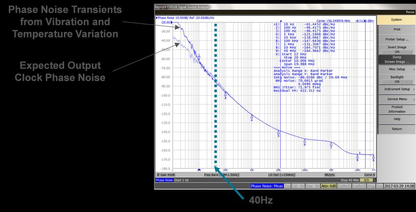
AN1077: Selecting the Right Clocks for Timing Synchronization Applications • Phase Noise, Jitter and Wander in Si534x Single-Reference Clocks

2.2 Single-Reference Clock Phase Noise with Crystal Input

Single-reference jitter attenuating clocks will attenuate phase noise that exists above the chosen PLL bandwidth. Therefore if a
bandwidth above 10 Hz is used, the device will attenuate jitter only. If a bandwidth below 10 Hz is used, the device will attenuate both
wander and jitter. The magnitude of attenuation is determined by transfer function of the PLL, thus the attenuation is greater at higher
frequency offsets from the PLL bandwidth. Sources of phase noise in these types of clocks are summarized below:

• Above the PLL bandwidth, phase noise from the input clock is attenuated. Output clock phase noise is dominated by the quality of
  the reference crystal, oscillator circuit and VCO.
• Below the PLL bandwidth, there is no phase noise attenuation. Therefore the phase noise of the input clock is added to the phase
  noise floor from the oscillator circuit and VCO.

The following figure illustrates the sources of phase noise from a single-reference clock using a PLL bandwidth of 1 kHz:

                            Figure 2.3. Phase Noise Measured from Single-Reference Clocks with Crystal

              Skyworks Solutions, Inc. • Phone [781] 376-3000 • Fax [781] 376-3100 • sales@skyworksinc.com • www.skyworksinc.com
5        Rev. 0.1 • Skyworks Proprietary Information • Products and Product Information are Subject to Change Without Notice • July 26, 2021    5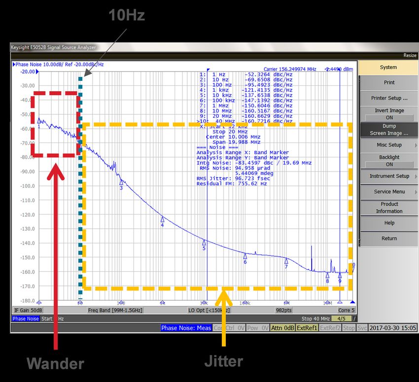
AN1077: Selecting the Right Clocks for Timing Synchronization Applications • Phase Noise, Jitter and Wander in Si534x Single-Reference Clocks

2.3 Single-Reference Clock Phase Noise with Oscillator Input

An oscillator, TCXO or OCXO may be connected to the XA/XB reference input on Si534x devices in lieu of a crystal. In this case, the
oscillator connected to XA/XB will determine the phase noise floor above the PLL bandwidth. Therefore the following recommendations
should be followed if it is desired to have low-jitter output clocks from Si534x when an oscillator is connected to the XA/XB pins:
 • A low-phase noise oscillator must be used
 • The clock output from the oscillator should have reasonably fast slew rates. For best performance, do not use device with a
   clipped-sine wave output. Instead, an oscillator with a CMOS output is recommended.

It should be emphasized that the jitter performance of most commercial oscillators will not match the jitter performance of the
Si534x. For the best jitter performance, Silicon Labs recommends using a crystal with single-reference clocks, or using one of the
dual-reference clocks described in the sections below.

                           Figure 2.4. Phase Noise Measured from Single-Reference Clocks with Oscillator

When using an oscillator connected to the XA/XB pins, be sure to check the Si534x datasheet limits for minimum and maximum input
frequency to be sure the oscillator’s output frequency can be supported.

              Skyworks Solutions, Inc. • Phone [781] 376-3000 • Fax [781] 376-3100 • sales@skyworksinc.com • www.skyworksinc.com
6        Rev. 0.1 • Skyworks Proprietary Information • Products and Product Information are Subject to Change Without Notice • July 26, 2021    6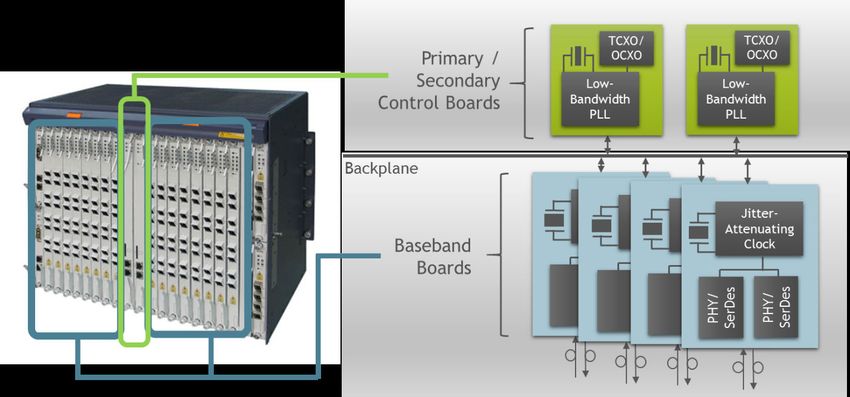
AN1077: Selecting the Right Clocks for Timing Synchronization Applications • Phase Noise, Jitter and Wander in Si534x Single-Reference Clocks

2.4 Wander Generation from Single-Reference Clocks

For bandwidths below 40 Hz, crystals can produce large phase noise transients caused by temperature variation and physical vibration.
These transients will result in poor output clock phase noise performance at offset frequencies below 40 Hz, as well as poor MTIE/
TDEV performance. This is sometimes referred to as “crystal wander generation” even though it affects jitter above 10 Hz as well. This
is illustrated in the figure below:

                         Figure 2.5. Phase Noise Performance with Crystal on XA/XB and Bandwidth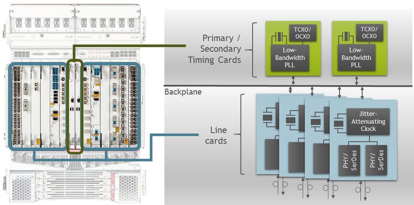
AN1077: Selecting the Right Clocks for Timing Synchronization Applications • Phase Noise, Jitter and Wander in Si534x Single-Reference Clocks

2.5 Holdover Frequency Averaging in Single-Reference Clocks

For applications including SyncE, SONET and SDH that require a PLL to enter holdover when a clock becomes invalid, the Si534x
devices offer historical frequency averaging to calculate the initial frequency offset during entry into holdover. The holdover circuit for
each DSPLL inside the Si534x stores up to 120 seconds of historical frequency data while locked to a valid clock input. This data uses
the XA/XB input as its reference. When entering holdover, the DSPLL will then pull its output clock frequency to the calculated average
historical frequency. This removes static frequency offsets that exist on the local oscillator connected to XA/XB, which provides greater
holdover accuracy.

In applications where a TCXO or OCXO is used with Si5342/4/5/6/7 single-reference clocks, the TCXO/OCXO must be connected to
the XA/XB reference input and NOT connected to a spare PLL input. Although it is possible to configure the Si534x to automatically
switch between clock inputs when one fails, connecting the TCXO/OCXO to a free PLL input has the following drawbacks:
 • The holdover frequency averaging feature will not be available to provide a frequency offset during entry into holdover. This will
   make it difficult to meet the holdover accuracy requirements for SyncE/SONET/SDH and may result in large output clock phase
   transients when entering and exiting holdover.
 • If the PLL bandwidth is below 40 Hz, wander performance will be poor due to the wander generation from the crystal (see previous
   section)
 • Applying a TCXO/OCXO a clock input reduces the number of inputs available for other clocks

                Figure 2.7. TCXO/OCXO Connection to Si5342/4/5/6/7 for Holdover Support in SyncE/SONET/SDH

              Skyworks Solutions, Inc. • Phone [781] 376-3000 • Fax [781] 376-3100 • sales@skyworksinc.com • www.skyworksinc.com
8        Rev. 0.1 • Skyworks Proprietary Information • Products and Product Information are Subject to Change Without Notice • July 26, 2021    8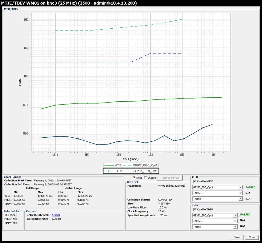
AN1077: Selecting the Right Clocks for Timing Synchronization Applications • Phase Noise, Jitter and Wander in Silicon Labs Dual-Reference Clocks

3. Phase Noise, Jitter and Wander in Silicon Labs Dual-Reference Clocks

3.1 Dual-Reference Network Synchronizer Clock Definition

Silicon Labs products like the Si5348/83/84 are considered to be “dual reference” clocks since they have two inputs for a crystal and
oscillator – one connected to the XA/XB pins and another connected to the REF/REFb pins. A crystal is connected to the XA/XB
pins and this determines the jitter performance of the device at offsets above 100 Hz. A TCXO or OCXO is typically connected to the
REF/REFb pins and this determines both the frequency stability of the device as well as the jitter and wander performance below 100
Hz. These devices are typically used for network synchronization applications such as SyncE and SONET/SDH.

                                                   TCXO/OCXO

                                                                                  XTAL

                                                    REF         REFb        XA              XB

                                                                                  OSC

                                           INx                                                      OUTx
                                                                                    ÷
                                                          DSPLL

                                 Figure 3.1. Si5348/83/84 Dual-Reference Network Synchronizer Clock

3.2 Dual-Reference Clock Phase Noise with Crystal and TCXO/OCXO Inputs

Unlike those of competitors, Silicon Labs' dual-reference clocks offer the advantage of using a TCXO/OCXO to provide frequency
stability without the TCXO/OCXO affecting the 12 kHz to 20 MHz jitter performance of the device. Sources of phase noise in these
types of devices are divided into three categories:
 • Above 100 Hz, phase noise from the input clock is attenuated. Output clock phase noise is dominated by the quality of the reference
   crystal, oscillator circuit and VCO.
 • Between the PLL bandwidth and 100 Hz, phase noise from the input clock is also attenuated. However the output clock phase noise
   is primarily determined by the phase noise of the TCXO/OCXO connected to the REF/REFb pins and the VCO.
 • Below the PLL bandwidth, there is no phase noise attenuation. Therefore the phase noise of the input clock is added to the phase
   noise floor from the VCO.

This is illustrated in Figure 3.2 Phase Noise Measured from Dual-Reference Clocks on page 10.

              Skyworks Solutions, Inc. • Phone [781] 376-3000 • Fax [781] 376-3100 • sales@skyworksinc.com • www.skyworksinc.com
9        Rev. 0.1 • Skyworks Proprietary Information • Products and Product Information are Subject to Change Without Notice • July 26, 2021        9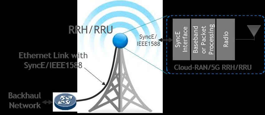
AN1077: Selecting the Right Clocks for Timing Synchronization Applications • Phase Noise, Jitter and Wander in Silicon Labs Dual-Reference Clocks

                                     Figure 3.2. Phase Noise Measured from Dual-Reference Clocks

Although two external components are required, the dual-reference clocks offer the following advantages over the single-reference
clocks:
 • Jitter above 100 Hz is not affected by the TCXO/OCXO. Therefore an additional jitter attenuator is not required on the PCB to
   provide low-jitter clocks for SerDes and other components.
 • Below 100 Hz, the PLL takes advantage of the low jitter annd wander from the TCXO/OCXO reference, and the TCXO/OCXO
   provides a stable reference for holdover.
 • A wide range of TCXO/OCXO output frequencies are supported: 5 to 250 MHz
 • Silicon Labs' dual-reference clocks support 1 PPS/1 Hz frequencies

3.3 Holdover Frequency Averaging in Dual-Reference Clocks

Silicon Labs’ dual-reference clocks use the REF/REFb reference input (not the XA/XB input) as the reference for holdover frequency
averaging. Therefore, the calculated frequency offsets for holdover entry will use the stable TCXO/OCXO reference.

              Skyworks Solutions, Inc. • Phone [781] 376-3000 • Fax [781] 376-3100 • sales@skyworksinc.com • www.skyworksinc.com
10       Rev. 0.1 • Skyworks Proprietary Information • Products and Product Information are Subject to Change Without Notice • July 26, 2021        10
AN1077: Selecting the Right Clocks for Timing Synchronization Applications • Recommended DSPLL Devices for Various Timing Architectures
4. Recommended DSPLL Devices for Various Timing Architectures
4.1 Distributed Timing Architecture
High-performance telecommunications equipment such as core and metro routers supporting SyncE/SONET/SDH typically employ a
distributed timing architecture:
• Redundant primary and secondary timing cards each use a low-bandwidth PLL with stable TCXO/OCXO reference. This is used to
attenuate wander and jitter from incoming recovered clocks, and provide standards-compliant frequency stability during holdover.
• Fanout buffers distribute recovered clocks to individual line cards over a backplane.
• Line cards each contain a jitter-attenuating clock to remove backplane jitter and provide a clean clock to each of the PHY/SerDes
devices.
Figure 4.1. Distributed Timing Architecture
Some typical loop bandwidth requirements for timing cards are given below:
Table 4.1. Typical Loop Bandwidth Requirements
SONET (Telcordia) SDH (ITU-T) SyncE (ITU-T) Loop Bandwidth
GR-253 Stratum 3E G.812 Type III — 0.001 Hz
GR-253 Stratum 3 G.812 Type IV G.8262 EEC Option 2AN1077: Selecting the Right Clocks for Timing Synchronization Applications • Recommended DSPLL Devices for Various Timing Architectures
4.2 Recommended DSPLLs for Timing Card Designs
In order to support low PLL bandwidths and stable frequency performance, a TCXO or OCXO is required for timing card designs. In
addition to the TCXO/OCXO, timing cards may need to support 1Hz/1PPS frequencies. For these reasons Silicon Labs recommends
the use of dual-reference network synchronizers such as Si5348/83/84 for timing card designs.
• Phase noise performance above 100Hz is not affected by the TCXO/OCXO. There-
fore a lower-cost TCXO/OCXO can be used and an additional jitter attenuator is not
required on the PCB*
• Lower power consumption than competing devices
• A wide range of TCXO/OCXO output frequencies are supported: 5 to 250 MHz
• Support for 1 Hz/1 PPS output (Si5348) and 1 Hz/1 PPS input (Si5383/84)
Figure 4.2. Si5348/83/84 Dual-Reference Clocks Recommended for Timing Card Designs
*Note: Jitter performance is less critical for timing card clocks since each line card will have its own jitter attenuating clock. However,
Si5348/83/84 can provide low-jitter clocks if required for other timing card devices without the need for an additional jitter attenuator.
4.3 Recommended DSPLLs for Line Card Designs
Line card clocks attenuate jitter (not wander) and provide switching between the primary and secondary timing card inputs. Loop
bandwidths >10 Hz are typically used. The jitter performance of line card clocks is critical since these clocks are used as the input to
PHY/SerDes components.
Silicon Labs recommends the use of single-reference jitter attenuators such as Si5342/4/5/6/7 for line card designs.
• Industry’s lowest jitter, which is ideal for high-speed PHY/SerDes clocking
• MultiSynth fractional synthesizers offer the greatest frequency flexibility and 0ppm
frequency synthesis error
• DSPLL technology is not susceptible to PLL crosstalk or power supply noise
• Lower power consumption than competing devices
Figure 4.3. Si5342/4/5/6/7 Recommended for Line Card Designs
If desired, an oscillator can be used in lieu of a crystal for the XA/XB input to Si534x but it is necessary to use a low-jitter oscillator
for line card designs. As mentioned above, the output clock jitter of Si534x is dependent on the jitter performance of the oscillator.
Skyworks Solutions, Inc. • Phone [781] 376-3000 • Fax [781] 376-3100 • sales@skyworksinc.com • www.skyworksinc.com
12 Rev. 0.1 • Skyworks Proprietary Information • Products and Product Information are Subject to Change Without Notice • July 26, 2021 12AN1077: Selecting the Right Clocks for Timing Synchronization Applications • Recommended DSPLL Devices for Various Timing Architectures
4.4 Centralized Timing/"Pizza Box" Architecture
Smaller telecommunications equipment is often designed to fit in a 1U or 2U rack space. These designs may use a single PCB which
must support all of the functions of the distributed timing architecture:
• A low-bandwidth PLL with stable TCXO/OCXO reference. This is used to attenuate wander and jitter from incoming recovered
clocks, and provide standards-compliant frequency accuracy during holdover.
• Low-jitter PLL(s) and fanout buffers to provide clean clocks to each of the PHY/SerDes devices
If the low-bandwidth PLL does not provide sufficient jitter performance, an additional PLL can be used for jitter attenuation.
Figure 4.4. Centralized Timing / “Pizza Box” Architecture
4.5 Recommended DSPLLs for Centralized Timing/"Pizza Box" Architecture
As with timing cards, centralized timing designs require a TCXO or OCXO for low PLL bandwidths and stable frequency performance.
1Hz/1PPS frequencies may also be present. In addition, low-jitter clocks are needed for PHY/SerDes clocking. For these reasons
Silicon Labs recommends the use of dual-reference network synchronizers such as Si5348/83/84 for “pizza box” designs.
• Industry’s lowest jitter, which is ideal for high-speed PHY/
SerDes clocking
• Phase noise performance above 100 Hz is not affected by the
TCXO/OCXO. Therefore a low-cost TCXO/OCXO can be used
and an additional jitter attenuator is not required on the PCB.
• DSPLL technology is not susceptible to PLL crosstalk or power
supply noise
• Lower power consumption than competing devices
• A wide range of TCXO/OCXO frequencies are supported: 5 to
250 MHz
• Support for 1 Hz/1 PPS output (Si5348) and 1 Hz/1 PPS input
(Si5383/84)
Figure 4.5. Si5348/83/84 Recommended for “Pizza Box” Designs
Skyworks Solutions, Inc. • Phone [781] 376-3000 • Fax [781] 376-3100 • sales@skyworksinc.com • www.skyworksinc.com
13 Rev. 0.1 • Skyworks Proprietary Information • Products and Product Information are Subject to Change Without Notice • July 26, 2021 13AN1077: Selecting the Right Clocks for Timing Synchronization Applications • Recommended DSPLL Devices for Various Timing Architectures
4.6 Wireless Base Station/BBU/eNodeB Applications
Wireless base station applications often have a distributed architecture similar to section 4.1 Distributed Timing Architecture above.
“Control boards” are similar to timing cards and the clock devices must attenuate wander and jitter, and provide a stable frequency
reference. “Baseband boards” are similar to line cards and the clock devices must switch between redundant control boards, attenuate
backplane jitter and provide clean clocks to PHY/SerDes devices. Phase alignment of output clocks may also be needed on baseband
boards.
Figure 4.6. Wireless Base Station / BBU / eNodeB Architecture
Skyworks Solutions, Inc. • Phone [781] 376-3000 • Fax [781] 376-3100 • sales@skyworksinc.com • www.skyworksinc.com
14 Rev. 0.1 • Skyworks Proprietary Information • Products and Product Information are Subject to Change Without Notice • July 26, 2021 14AN1077: Selecting the Right Clocks for Timing Synchronization Applications • Recommended DSPLL Devices for Various Timing Architectures
4.7 Recommended Clocks for Wireless Base Station/BBU/eNodeB Applications
As with timing cards, Silicon Labs recommends the use of dual-reference network synchronizers such as Si5348/83/84 for wireless
base station control board designs. The Si5348/83/84 offers superior performance with a stable TCXO/OCXO reference, and supports
for 1 PPS/1 Hz frequencies.
• Phase noise performance above 100Hz is not affected by the TCXO/OCXO. There-
fore a low-cost TCXO/OCXO can be used and an additional jitter attenuator is not
required on the PCB.
• A wide range of TCXO/OCXO output frequencies are supported: 5 to 250 MHz
• Support for 1Hz/1PPS output (Si5348) and 1Hz/1PPS input (Si5383/84)
Figure 4.7. Si5348/83/84 Recommended for Wireless Base Station Control Boards
Silicon Labs recommends the use of single-reference jitter attenuators such as Si5342/4/5 for wireless baseband boards. These
devices offer the industry’s best jitter performance and can provide low input-to-output skew when used in zero delay mode. The output
delay/skew is also adjustable which can compensate for different PCB trace delays. (Note Si5346/7 do not offer zero delay mode or
adjustable output delay.)
• Industry’s lowest jitter, which is ideal for high-speed PHY/SerDes clocking
• Low input-to-output skew (with zero delay mode), and adjustable output skew
• MultiSynth fractional synthesizers offer the greatest frequency flexibility and 0ppm
frequency synthesis error
• DSPLL technology is not susceptible to power supply noise
• Lower power consumption than competing devices
Figure 4.8. Si5342/4/5 Recommended for Wireless Base Station Baseband Boards
Skyworks Solutions, Inc. • Phone [781] 376-3000 • Fax [781] 376-3100 • sales@skyworksinc.com • www.skyworksinc.com
15 Rev. 0.1 • Skyworks Proprietary Information • Products and Product Information are Subject to Change Without Notice • July 26, 2021 15AN1077: Selecting the Right Clocks for Timing Synchronization Applications • Recommended DSPLL Devices for Various Timing Architectures
4.8 Wireless Radio Interface (RRH and RRU) Applications
Radio interface devices for wireless infrastructure, sometimes referred to as remote radio head (RRH) or remote radio unit (RRU),
typically connect to base stations with a Common Public Radio Interface (CPRI) fronthaul link. The RRH/RRU then contains a CPRI
receiver and the radio interface:
Figure 4.9. Traditional 4G/LTE Wireless Fronthaul with CPRI
Emerging wireless infrastructure deployments including Cloud-RAN and 5G are now consolidating base station and radio interface
functionality into a single unit, while adding IEEE1588 for phase synchronization:
Figure 4.10. Emerging Cloud-RAN / 5G Radio Interface
Skyworks Solutions, Inc. • Phone [781] 376-3000 • Fax [781] 376-3100 • sales@skyworksinc.com • www.skyworksinc.com
16 Rev. 0.1 • Skyworks Proprietary Information • Products and Product Information are Subject to Change Without Notice • July 26, 2021 16AN1077: Selecting the Right Clocks for Timing Synchronization Applications • Recommended DSPLL Devices for Various Timing Architectures
As a result, CPRI fronthaul links are no longer required for Cloud-RAN/5G, and SyncE/1588 is connected directly to the RRH/RRU. This
presents a challenge to clock tree design due to dissimilar requirements of baseband and radio interface clocks:
Table 4.2. Typical Radio Interface vs. SyncE/1588 Baseband Clock Requirements
Typical SyncE/1588 Baseband Typical Radio Interface
Specification
Clock Requirements Clock Requirements
PLL Bandwidth Very lowAN1077: Selecting the Right Clocks for Timing Synchronization Applications • Recommended DSPLL Devices for Various Timing Architectures
4.10 Recommended Clocks for Cloud-RAN/5G Wireless Radio Interface (RRH and RRU) Applications
Given the dissimilar requirements for the SyncE/1588 baseband clocks and the radio interface clocks, Silicon Labs recommends two
clock devices for Cloud-RAN/5G RRH/RRU designs. The Si5348/83/84 should be used for the baseband in order to support the low
PLL bandwidth and stable TCXO/OCXO reference. For the radio interface the Si5380 should be used, as it provides the lowest close-in
phase noise as well as JESD204B clock phase alignment.
Figure 4.12. Radio Interface Clocking for Cloud-RAN / 5G
This arrangement offers advantages for both the baseband clock tree and the radio clock tree:
Baseband Clock Advantages with Si5348/83/84: Radio Clock Advantages with Si5380:
• Phase noise performance above 100 Hz is not affected by • No need for external VCXO or loop filter components
the TCXO/OCXO. Therefore a lower-cost TCXO/OCXO can • 67% reduction in PCB area versus competitors
be used and an additional jitter attenuator is not required on
• 32% reduction in power consumption versus competitors
the PCB.
• Supports JESD204B clocking for wireless ADCs/DACs
• A wide range of TCXO/OCXO output frequencies are
supported: 5 to 250 MHz
• Support for 1 Hz/1 PPS output (Si5348/83/84) and
1 Hz/1 PPS input (Si5383/84)
Skyworks Solutions, Inc. • Phone [781] 376-3000 • Fax [781] 376-3100 • sales@skyworksinc.com • www.skyworksinc.com
18 Rev. 0.1 • Skyworks Proprietary Information • Products and Product Information are Subject to Change Without Notice • July 26, 2021 18AN1077: Selecting the Right Clocks for Timing Synchronization Applications • Summary and Selection Guide
5. Summary and Selection Guide
With both single-reference and dual-reference clocks, Silicon Labs Si534x/8x devices provide flexible options to meet the needs of
today’s synchronization designs. The selection guide below summarizes Silicon Labs’ recommendations for various application types.
Figure 5.1. Synchronization Clock Selection Guide
Skyworks Solutions, Inc. • Phone [781] 376-3000 • Fax [781] 376-3100 • sales@skyworksinc.com • www.skyworksinc.com
19 Rev. 0.1 • Skyworks Proprietary Information • Products and Product Information are Subject to Change Without Notice • July 26, 2021 19ClockBuilder Pro
Customize Skyworks clock generators,
jitter attenuators and network
synchronizers with a single tool. With
CBPro you can control evaluation
boards, access documentation, request
a custom part number, export for
in-system programming and more!
www.skyworksinc.com/CBPro
Portfolio SW/HW Quality Support & Resources
www.skyworksinc.com/ia/timing www.skyworksinc.com/CBPro www.skyworksinc.com/quality www.skyworksinc.com/support
Copyright © 2021 Skyworks Solutions, Inc. All Rights Reserved.
Information in this document is provided in connection with Skyworks Solutions, Inc. (“Skyworks”) products or services. These materials, including the
information contained herein, are provided by Skyworks as a service to its customers and may be used for informational purposes only by the customer.
Skyworks assumes no responsibility for errors or omissions in these materials or the information contained herein. Skyworks may change its documentation,
products, services, specifications or product descriptions at any time, without notice. Skyworks makes no commitment to update the materials or
information and shall have no responsibility whatsoever for conflicts, incompatibilities, or other difficulties arising from any future changes.
No license, whether express, implied, by estoppel or otherwise, is granted to any intellectual property rights by this document. Skyworks assumes no liability
for any materials, products or information provided hereunder, including the sale, distribution, reproduction or use of Skyworks products, information or
materials, except as may be provided in Skyworks’ Terms and Conditions of Sale.
THE MATERIALS, PRODUCTS AND INFORMATION ARE PROVIDED “AS IS” WITHOUT WARRANTY OF ANY KIND, WHETHER EXPRESS, IMPLIED, STATUTORY, OR
OTHERWISE, INCLUDING FITNESS FOR A PARTICULAR PURPOSE OR USE, MERCHANTABILITY, PERFORMANCE, QUALITY OR NON-INFRINGEMENT OF ANY
INTELLECTUAL PROPERTY RIGHT; ALL SUCH WARRANTIES ARE HEREBY EXPRESSLY DISCLAIMED. SKYWORKS DOES NOT WARRANT THE ACCURACY OR
COMPLETENESS OF THE INFORMATION, TEXT, GRAPHICS OR OTHER ITEMS CONTAINED WITHIN THESE MATERIALS. SKYWORKS SHALL NOT BE LIABLE FOR
ANY DAMAGES, INCLUDING BUT NOT LIMITED TO ANY SPECIAL, INDIRECT, INCIDENTAL, STATUTORY, OR CONSEQUENTIAL DAMAGES, INCLUDING WITHOUT
LIMITATION, LOST REVENUES OR LOST PROFITS THAT MAY RESULT FROM THE USE OF THE MATERIALS OR INFORMATION, WHETHER OR NOT THE RECIPIENT
OF MATERIALS HAS BEEN ADVISED OF THE POSSIBILITY OF SUCH DAMAGE.
Skyworks products are not intended for use in medical, lifesaving or life-sustaining applications, or other equipment in which the failure of the Skyworks
products could lead to personal injury, death, physical or environmental damage. Skyworks customers using or selling Skyworks products for use in such
applications do so at their own risk and agree to fully indemnify Skyworks for any damages resulting from such improper use or sale.
Customers are responsible for their products and applications using Skyworks products, which may deviate from published specifications as a result of
design defects, errors, or operation of products outside of published parameters or design specifications. Customers should include design and operating
safeguards to minimize these and other risks. Skyworks assumes no liability for applications assistance, customer product design, or damage to any
equipment resulting from the use of Skyworks products outside of Skyworks’ published specifications or parameters.
Skyworks, the Skyworks symbol, Sky5®, SkyOne®, SkyBlue™, Skyworks Green™, Clockbuilder®, DSPLL®, ISOmodem®, ProSLIC®, and SiPHY® are trademarks or
registered trademarks of Skyworks Solutions, Inc. or its subsidiaries in the United States and other countries. Third-party brands and names are for
identification purposes only and are the property of their respective owners. Additional information, including relevant terms and conditions, posted at
www.skyworksinc.com, are incorporated by reference.
Skyworks Solutions, Inc. | Nasdaq: SWKS | sales@skyworksinc.com | www.skyworksinc.com
USA: 781-376-3000 | Asia: 886-2-2735 0399 | Europe: 33 (0)1 43548540 |You can also read