Application Note GreenPAK based AC-Power Phase Cut Control with System Monitoring Features
←
→
Page content transcription
If your browser does not render page correctly, please read the page content below
Application Note
    GreenPAK based AC-Power
   Phase Cut Control with System
       Monitoring Features
                                     AN-CM-305

Abstract
This application note describes a GreenPAK™ based solution to control AC-Power with a phase cut
logic along with system monitoring features. A push button controls 2 phase delays programmed on-
chip at hardware level, and an I2C compatible MCU modifies the phase delays at software level via
I2C. The solution can be expanded to include more programmed delays for hardware control and
additional system monitoring features.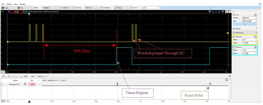
AN-CM-305
GreenPAK based AC-Power Phase Cut Control with
System Monitoring Features

Contents
Abstract ................................................................................................................................................ 1
Contents ............................................................................................................................................... 2
Figures .................................................................................................................................................. 2
Tables ................................................................................................................................................... 3
1    Terms and Definitions ................................................................................................................... 4
2    References ..................................................................................................................................... 4
3    Introduction.................................................................................................................................... 5
4    Zero-Crossing Circuit ................................................................................................................... 5
5    GreenPAK Design ......................................................................................................................... 7
     5.1 Hardware Control .................................................................................................................. 8
     5.2 Software Control ................................................................................................................... 8
     5.3 System Monitoring Features ................................................................................................. 9
          5.3.1   Over Temperature Protection .............................................................................. 10
          5.3.2   Emergency Shutdown .......................................................................................... 11
          5.3.3   Watchdog Timer .................................................................................................. 11
          5.3.4   Frequency Detector ............................................................................................. 12
     5.4 Modifying the Phase Delay ................................................................................................. 13
6    TRIAC Driver Circuit .................................................................................................................... 13
7    Testing .......................................................................................................................................... 14
8    Feature Extension ....................................................................................................................... 14
9    Demonstration PCB .................................................................................................................... 16
10 Conclusion ................................................................................................................................... 17
Revision History ................................................................................................................................ 18

Figures
Figure 1: Phase Cut Output ................................................................................................................... 5
Figure 2: Opto-isolator with Phototransistor .......................................................................................... 6
Figure 3: Zero-Crossing Circuit Waveforms .......................................................................................... 6
Figure 4: GreenPAK Design .................................................................................................................. 7
Figure 5: Hardware Control Waveforms ................................................................................................ 8
Figure 6: Software Control Waveforms ................................................................................................. 9
Figure 7: OTP Schematic .................................................................................................................... 10
Figure 8: OTP Waveforms ................................................................................................................... 10
Figure 9: Emergency Shutdown .......................................................................................................... 11
Figure 10: Watchdog Timer ................................................................................................................. 12
Figure 11: Frequency Detector ............................................................................................................ 12
Figure 12: Photo-TRIAC Opto-isolator ................................................................................................ 13
Figure 13: Phase Cut Test Schematic ................................................................................................. 14
Figure 14: Software Control Phase Cut Output ................................................................................... 15
Figure 15: Hardware Control Phase Cut Output ................................................................................. 15
Figure 16: DA14531 USB Development Kit based Test Schematic ................................................... 16
Figure 17: Phase Cut and Cycle Skip PCB ......................................................................................... 16

Application Note                                                  Revision 1.0                                                          31-Mar-2021

CFR0014                                                                 2 of 19                                          © 2021 Dialog Semiconductor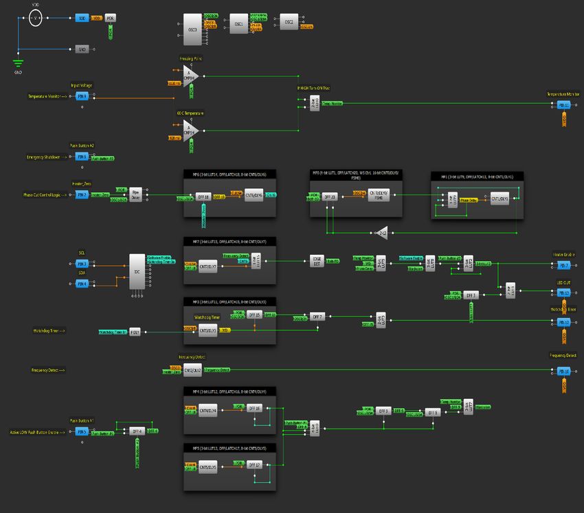
AN-CM-305
GreenPAK based AC-Power Phase Cut Control with
System Monitoring Features

Tables
Table 1: CNT0/DLY0 I2C Address ...................................................................................................... 13

Application Note                                         Revision 1.0                                                 31-Mar-2021

CFR0014                                                       3 of 19                                    © 2021 Dialog Semiconductor
AN-CM-305
GreenPAK based AC-Power Phase Cut Control with
System Monitoring Features

1      Terms and Definitions
AC                 Alternating Current
ACMP               Analog Comparators
I2C                Inter-Integrated Circuit Serial Communication
LED                Light Emitting Diode
LUT                Look Up Table
OTP                Over Temperature Protection
PCB                Printed Circuit Board
SCR                Silicon Controlled Rectifier
TRIAC              Triode for Alternating Current

2      References
For related documents and software, please visit:
https://www.dialog-semiconductor.com/greenpak
Download our free GreenPAK Designer Software [1] to open the .gp files [2] and view the proposed
circuit design. Use the GreenPAK Development Tools [3] to freeze the design into your own
customized IC in a matter of minutes. Dialog Semiconductor provides a complete library of
application notes [4] featuring design examples as well as explanations of features and blocks within
the Dialog IC.
[1]   GreenPAK Designer Software, Software Download and User Guide, Dialog Semiconductor.
[2]   AN-CM-305, GreenPAK based AC-Power Cycle Skip Control with System Monitoring Features,
      GreenPAK Design File, Dialog Semiconductor.
[3]   GreenPAK Development Tools, GreenPAK Development Tools Webpage, Dialog
      Semiconductor.
[4]   GreenPAK Application Notes, GreenPAK Application Notes Webpage, Dialog Semiconductor.
[5]   SLG46855, Datasheet, Dialog Semiconductor.

Author: Krupa Bhavsar

Application Note                           Revision 1.0                                   31-Mar-2021

CFR0014                                        4 of 19                         © 2021 Dialog Semiconductor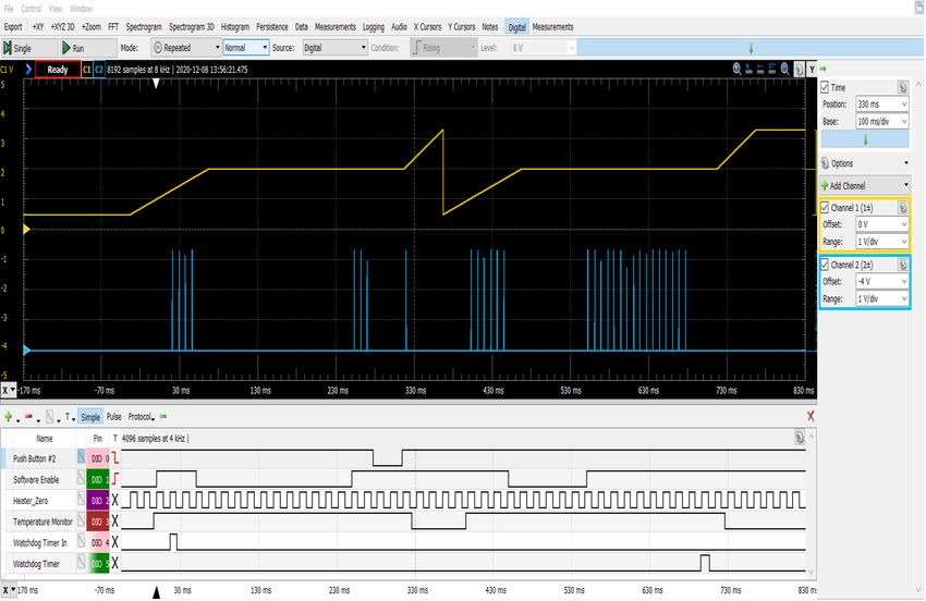
AN-CM-305
GreenPAK based AC-Power Phase Cut Control with
System Monitoring Features

3     Introduction
Most home-based electrical appliances generally use AC power for operation. Phase cut logic can be
used in appliances such as AC dimmers and light bulbs. These electrical appliances consist of power
electronic switches like Silicon Controlled Rectifier (SCR)s, and Triode for Alternating Current
(TRIAC)s which are turned ON/OFF periodically to achieve smooth operation.
In this control, the load is turned ON for a portion of half cycle and is turned OFF for a portion of half
cycle. This phenomenon of turning ON for a portion of a cycle reduces the overall power
consumption. Figure 1 displays the phase cut logic output. As shown in Figure 1, the load is turned
ON for a fraction of a cycle in each direction and is turned OFF for a part of a cycle in each direction.
The load is completely turned OFF at each zero-crossing due to the property of TRIACs which is
described in detail in 6.
Channel 1 (blue/top line) - AC Supply
Channel 2 (green/bottom line) - Phase Cut Output

                                      Figure 1: Phase Cut Output

This application note is divided into 3 sections. 4 describes a zero-crossing circuit, 5 illustrates the
generation of different phase delays including system monitoring features using GreenPAK [5], and 6
defines a TRIAC driver circuit for driving the load.

4     Zero-Crossing Circuit
A zero-crossing circuit consists of an AC power supply, a half-wave rectifier, and an opto-isolator with
a photo-sensitive device - phototransistor. The opto-isolators isolate AC and DC signals using light.
This opto-isolator consists of a LED, a light beam, and phototransistor as shown in Figure 2. The
half-wave rectifier rectifies the HIGH voltage AC input and feeds the rectified output to the input LED
of the opto-isolator. The signal from the LED then travels with an intensity proportional to the input
signal, and falls onto the base of the phototransistor which in turn triggers the phototransistor to the

Application Note                             Revision 1.0                                     31-Mar-2021

CFR0014                                          5 of 19                           © 2021 Dialog Semiconductor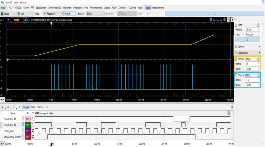
AN-CM-305
GreenPAK based AC-Power Phase Cut Control with
System Monitoring Features
ON state. The output of the phototransistor is a DC signal, which is used for generating different
patterns in GreenPAK.
Figure 2: Opto-isolator with Phototransistor
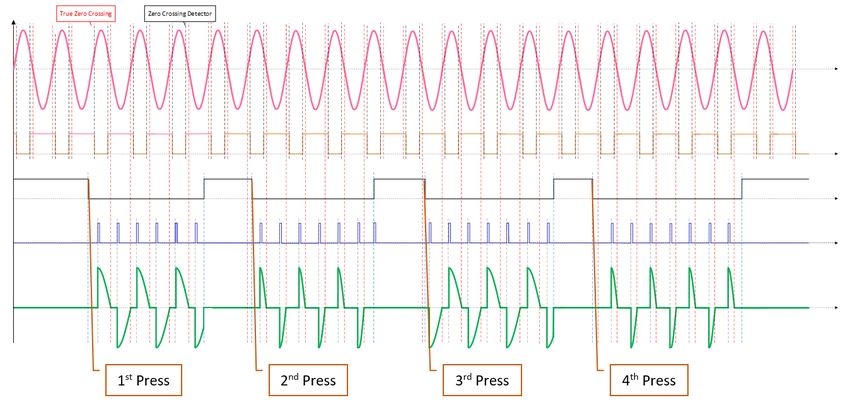
Figure 3 displays the zero-crossing circuit waveforms. As seen in Figure 3, the DC signal at the
phototransistor output is triggered before and after the true zero-crossing. The true zero-crossing is
defined as the exact time when the AC signal reaches a zero voltage. This time shift is compensated
inside the GreenPAK and the phase delays are adjusted accordingly.
Channel 1(blue/top line) - AC Supply
Channel 2 (green/2nd line) - Half Wave Rectifier Output
Channel 3 (yellow/bottom line) - Opto-Isolator Output
Figure 3: Zero-Crossing Circuit Waveforms
Application Note Revision 1.0 31-Mar-2021
CFR0014 6 of 19 © 2021 Dialog Semiconductor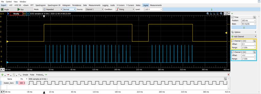
AN-CM-305
GreenPAK based AC-Power Phase Cut Control with
System Monitoring Features

5     GreenPAK Design
Figure 4 reveals the GreenPAK Design for generating various phase delays for driving the load along
with system monitoring features. This GreenPAK design can be used worldwide as it supports both
50Hz and 60Hz AC frequencies. This design includes both controls (i.e. hardware and software).

                                    Figure 4: GreenPAK Design

The phototransistor output of the zero-crossing circuit arrives at Heater_Zero (Pin 2) of GreenPAK.
As shown in Figure 3, the DC signal at the phototransistor output is triggered ON before the high
voltage AC signal reaches it's true zero-crossing. So, the rising edge of the phototransistor output is
delayed internally, and the pulse width of the input signal is calculated based on the frequency of the
input signal i.e. 50Hz and 60Hz.
5.1 describes the hardware control, 5.2 illustrates the software control, and 5.3 depicts the system
monitoring features. After the phase delays are generated, they are then routed and displayed on
Heater_Enable (Pin7). This Heater_Enable (Pin 7) is then connected to the TRIAC driving circuit for
driving the load.

Application Note                            Revision 1.0                                   31-Mar-2021

CFR0014                                         7 of 19                         © 2021 Dialog Semiconductor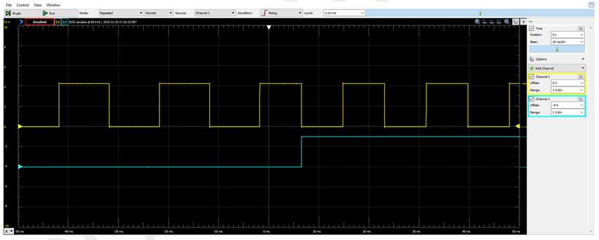
AN-CM-305
GreenPAK based AC-Power Phase Cut Control with
System Monitoring Features

5.1       Hardware Control
The hardware control technique requires an external active LOW push-button and is connected to
Push_Button #1 (Pin 5) on GreenPAK.
CNT4/DLY4 (3ms) and CNT5/DLY5 (5ms) are used to program 2 phase delays on-chip. Each phase
delay has 8-bit resolution and is user selectable. These phase delays are compatible with both input
frequencies i.e. 50Hz and 60Hz. Alternate toggle of the push button displays the same phase delay
on the Heater_Enable (Pin 7) only when the system monitoring features - Over Temperature
Protection (OTP) and Emergency Shutdown, are in range.
Figure 5 exhibits the hardware control waveforms. As seen in Figure 5, a zero-crossed AC signal
arrives at Heater_Enable (Pin 2), and at each alternate button press (Push Button #1 - Pin 5) the
same phase delay is propagated on the Heater_Enable (Pin 7). The Heater_Enable (Pin 7) is held
LOW when the button is released or when the system monitoring features are out of range.
Channel 1 (yellow/top line) – PIN#9 (Input Voltage)
Channel 2 (blue/2nd line) – PIN#7 (Heater_Enable)
D0 – PIN#6 (Push Button #2)
D1 – PIN#5 (Push Button #1)
D2 – PIN#2 (Heater_Zero)
D3 – PIN#11 (Temperature Monitor)

                               Figure 5: Hardware Control Waveforms

5.2       Software Control
The software control operates through an I2C communication from an external I2C compatible MCU.
In this control, the control data register of CNT0/DLY0 (16-bit resolution) is modified via I2C. After an
appropriate phase delay is written through I2C, the phase delay is routed and displayed on
Heater_Enable (Pin 7), as long as all the system monitoring features - Emergency Shutdown, OTP,
and Watchdog Timer are in range. 5.4 defines the recommended steps to modify the CNT0/DLY0
control data register via I2C.
Figure 6 reveals the software control waveforms. As shown in Figure 6, the phase delay is only
displayed on Heater_Enable (Pin 7) when Software Enable is HIGH and all system monitoring
features are in range.

Application Note                            Revision 1.0                                     31-Mar-2021

CFR0014                                          8 of 19                          © 2021 Dialog Semiconductor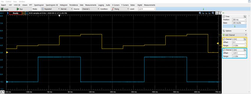
AN-CM-305
GreenPAK based AC-Power Phase Cut Control with
System Monitoring Features

5.3       System Monitoring Features
OTP, Emergency Shutdown, Watchdog Timer, and Frequency Detector are the system monitoring
features included in this GreenPAK design.
Channel 1 (yellow/top line) – PIN#9 (Input Voltage)
Channel 2 (blue/2nd line) – PIN#7 (Heater_Enable)
D0 – PIN#6 (Push Button #2)
D1 – I2C Virtual Input 0 - OUT0 (Software Enable)
D2 – PIN#2 (Heater_Zero)
D3 – PIN#11 (Temperature Monitor)
D4 – I2C Virtual Input 1 - OUT1 (Watchdog Timer In)
D5 – PIN#12 (Watchdog Timer)

                             Figure 6: Software Control Waveforms

Application Note                         Revision 1.0                             31-Mar-2021

CFR0014                                      9 of 19                   © 2021 Dialog Semiconductor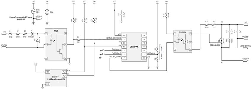
AN-CM-305
GreenPAK based AC-Power Phase Cut Control with
System Monitoring Features

5.3.1     Over Temperature Protection
OTP feature is available in both hardware and software control techniques. This feature requires an
external resistor divider with a thermistor. A thermistor is a temperature dependent resistor, whose
resistance decreases with increase in temperature.

                                     Figure 7: OTP Schematic

Figure 7 shows the OTP schematic. The sensed voltage is connected to Input Voltage (PIN 9) on
GreenPAK. The temperature range inside GreenPAK is accomplished with a set of 2 Analog
Comparators (ACMP)s and a LUT. In this design, the operational temperature range is set from 0˚C
to 60˚C, which respectively corresponds to a voltage range from 2.176V to 0.928V for ACMPs. When
the temperature is out of range the system is OFF, and when the temperature is in range, the design
functions according to the chosen user control, i.e. hardware or software.
Figure 8 displays the OTP waveforms. As seen in Figure 8, the temperature monitor output is HIGH
when the temperature is in range, and the output is LOW when the temperature is out of range.
Channel 1 (yellow/top line) – PIN# 9 (Input Voltage)
Channel 2 (blue/bottom line) – PIN# 11 (Temperature Monitor)

                                     Figure 8: OTP Waveforms

Application Note                           Revision 1.0                                   31-Mar-2021

CFR0014                                       10 of 19                         © 2021 Dialog Semiconductor
AN-CM-305
GreenPAK based AC-Power Phase Cut Control with
System Monitoring Features
5.3.2 Emergency Shutdown
Emergency shutdown has the highest priority and this feature is available for both hardware and
software control techniques. This feature is accomplished with an external active LOW push button
which is connected to Push Button #2 (Pin 6) on GreenPAK IC. When the button is pressed the
Heater_Enable (Pin 7) output goes LOW and the system turns OFF. When the button is released, the
system turns back ON depending upon software or hardware control and if other system monitoring
features are in range.
Channel 1 (yellow/top line) – PIN# 6 (Push Button #2)
Channel 2 (blue/bottom line) – PIN# 7 (Heater_Enable)
D0 – PIN# 2 (Heater_Zero)
Figure 9: Emergency Shutdown
Figure 9 depicts the emergency shutdown feature. As shown in Figure 9, when the button is pressed
the output at Heater_Enable (Pin 7) goes LOW.
5.3.3 Watchdog Timer
This feature is available in software control only and is controlled through an I2C compatible MCU.
CNT3 (8-bit) sets the period of the watchdog timer. At POR, CNT3 is loaded with a period
determined by its control data register, which is 656.25ms (default). The timer operates continuously
through a toggled I2C Virtual Input 1 - OUT1. If the MCU freezes or the I2C Virtual Input 1 - OUT1 is
toggled after the default set time, then the timer expires after 656.25ms and produces a reset pulse
at watchdog timer (Pin 12). When the timer expires, the Heater_Enable (Pin 7) goes LOW and the
system turns OFF. The timer period is user selectable and can be changed through I2C.
Channel 1 (yellow/top line) – (I2C Virtual Input 1 - OUT1)
Channel 2 (blue/bottom line) – (CNT3 Output)
D0 – PIN# 12(Watchdog Timer)
Application Note Revision 1.0 31-Mar-2021
CFR0014 11 of 19 © 2021 Dialog SemiconductorAN-CM-305
GreenPAK based AC-Power Phase Cut Control with
System Monitoring Features
Figure 10: Watchdog Timer
Figure 10 shows the watchdog timer waveforms. As shown in Figure 10, when the I2C Virtual Input 1
- OUT1 is toggled before 656.25ms, the watchdog timer output goes LOW and indicates the timer is
in range. When the I2C Virtual Input 1 - OUT1 is toggled after the default time of CNT3, then the
timer expires after 656.25ms (default) and the watchdog timer output produces a reset pulse.
Channel 1 (yellow/top line) – PIN# 2 (Heater_Zero)
Channel 2 (blue/bottom line) – PIN# 10 (Frequency Detect)
Figure 11: Frequency Detector
5.3.4 Frequency Detector
CNT2 is used to detect the frequency of the input signal. The frequency detect output is HIGH when
a consecutive edge of the input signal arrives before the set counter period, and frequency detect
output is LOW when a consecutive edge arrives later than the set counter period.
Figure 11 displays the frequency detector output. As seen in Figure 11, the frequency detect output
is LOW when the input signal frequency is 50Hz, and the output is HIGH when the input signal
frequency is 60Hz.
Application Note Revision 1.0 31-Mar-2021
CFR0014 12 of 19 © 2021 Dialog SemiconductorAN-CM-305
GreenPAK based AC-Power Phase Cut Control with
System Monitoring Features
5.4 Modifying the Phase Delay
For a specific power consumption, different phase delays are written in CNT0/DLY0 macrocell via
I2C. To re-write different phase delays the following steps are recommended.
1. Assert Software_Enable (I2C Virtual Input 0 - OUT0) LOW
2. Write a new phase delay time on CNT0/DLY0 registers
3. Assert Software_Enable HIGH
Following these steps in sequence guarantees proper synchronization of the new data written in
CNT0/DLY0 registers. Table 1 describes the I2C address of the CNT0/DLY0 macrocell.
Table 1: CNT0/DLY0 I2C Address
I2C Address CNT0/DLY0 Data Bits
0x95
D[15:0]
0x96
6 TRIAC Driver Circuit
The TRIAC driver circuit consists of an opto-isolator with photo-TRIAC and TRIAC for driving the
load.
Figure 12 shows the opto-isolator with photo-TRIAC. As indicated in Figure 12, the opto-isolator is
comprised of a LED and a photo-sensitive device, photo-TRIAC. This isolator isolates DC and AC
signals. The phase delays generated by the GreenPAK device are connected to the input LED of the
opto-isolator. These signals travel by LED emission and fall onto the gate of the photo-TRIAC.
Figure 12: Photo-TRIAC Opto-isolator
The outputs of the photo-TRIAC are connected to the power TRIAC, which is then connected to the
load. A positive pulse at the gate of TRIAC triggers it into the ON state. The property of a TRIAC is
that it automatically turns OFF at each half cycle of the sinusoidal supply voltage as the
instantaneous voltage and load current falls to zero. The TRIAC starts latching the data once again
at the next half cycle. The TRIAC can be turned OFF by either reducing the current across its
terminals below its minimum holding current, or when the supply voltage is cut-off. The signal at the
power TRIAC is the desired phase cut output of the input AC signal.
Application Note Revision 1.0 31-Mar-2021
CFR0014 13 of 19 © 2021 Dialog SemiconductorAN-CM-305
GreenPAK based AC-Power Phase Cut Control with
System Monitoring Features
7 Testing
Figure 13 demonstrates the schematic of the phase cut logic using GreenPAK. The main
components of the test setup are a half-wave rectifier, an opto-isolator with phototransistor, a
GreenPAK, an opto-isolator with photo-TRIAC, and a TRIAC. The test schematic shows the opto-
isolators used for testing. The base of phototransistor is connected to GND to achieve a stable output
and reduce false triggering due to electrical noise.
As indicated in Figure 13, the input AC signal is applied across LIVE and Neutral terminals. The
output load is connected across Load_LIVE and Load_Neutral terminals. There are two external
buttons, each connected to Push Button #1 (Pin 5) and Push Button #2 (Pin 6) on GreenPAK. The
voltage across the resistor divider is connected to Input Voltage (Pin 9) on GreenPAK. An I2C
compatible MCU is also present for the software control of the design. MCU's SCL and SDA lines are
respectively connected to the GreenPAK's SCL and SDA lines through pull-up resistors.
Figure 13: Phase Cut Test Schematic
Figure 14 displays the software control phase cut outputs of the test schematic with the assumption
that all the system monitoring features are in range. Data on CNT0/DLY0 macrocell is written through
I2C by following the steps in 5.4. The phase delayed outputs are displayed on Heater_Enable (Pin 7)
according to the set phase delay on CNT0/DLY0, and appropriate phase cut outputs are also shown
in Figure 14. The phase cut outputs are present on the load only when Software Enable is HIGH.
Once software enable goes LOW, the phase cut output also goes LOW.
Figure 15 shows the hardware control phase cut outputs with the assumption that all system
monitoring features are in range. At each alternate button press, a pre-programmed phase delay is
routed to Heater_Enable (Pin 7) and appropriately displayed on the phase cut output. Once the
button is released, Heater_Enable (Pin 7) goes LOW and also the phase cut output.
8 Feature Extension
The GreenPAK can be configured with any MCU capable of communicating through I2C. DA14531
Smartbond Tiny Development Kit-USB consists of IOs that can be configured as open drain outputs
for I2C communication.
Channel 1 (magenta/top line) - (AC Input)
Channel 2 (yellow/2nd line) - PIN#2 (Heater_Zero)
Channel 3 (black/3rd line) - I2C Virtual Input 0 - OUT0 (Software Enable)
Channel 4 (blue/4th line) - PIN#7 (Heater_Enable)
Channel 5 (green/bottom line) - Cycle Skip Output
Application Note Revision 1.0 31-Mar-2021
CFR0014 14 of 19 © 2021 Dialog SemiconductorAN-CM-305
GreenPAK based AC-Power Phase Cut Control with
System Monitoring Features
Figure 14: Software Control Phase Cut Output
Channel 1 (magenta/top line) - (AC Input)
Channel 2 (yellow/2nd line) - PIN#2 (Heater_Zero)
Channel 3 (black/3rd line) - PIN#5 (Push Button #1)
Channel 4 (blue/4th line) - PIN#7 (Heater_Enable)
Channel 5 (green/bottom line) - Cycle Skip Output
Figure 15: Hardware Control Phase Cut Output
Figure 16 displays the test setup of phase cut logic using DA14531 USB Development Kit. The
power to DA14531 USB Development Kit is provided through a USB port in the kit. As exhibited in
Figure 16, P0_2 (Port 0 - Pin 2) and P0_8 (Port 0 - Pin 8) pins are respectively configured as SCL
and SDA for I2C communication. Please follow the steps in 5.4 to send I2C commands to
Application Note Revision 1.0 31-Mar-2021
CFR0014 15 of 19 © 2021 Dialog SemiconductorAN-CM-305
GreenPAK based AC-Power Phase Cut Control with
System Monitoring Features
GreenPAK's CNT0/DLY0 macrocell for modifying the phase delays. Similar results on the phase cut
outputs are obtained when I2C commands are supplied from the DA14531 USB Development Kit.
Figure 16: DA14531 USB Development Kit based Test Schematic
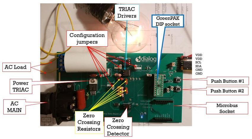
9 Demonstration PCB
Figure 17 shows the demonstration board for both phase cut and cycle skip logic. This PCB can be
readily used worldwide as the GreenPAK design supports both 50Hz and 60Hz AC frequencies. AC
mains supply is applied to the board through the AC mains connector. For demonstration, a light bulb
is used as a load.
Figure 17: Phase Cut and Cycle Skip PCB
The user needs to only connect the AC mains supply and load.
As evidenced from Figure 17, 2 separate TRIAC drivers and configuration jumpers are present on
the board to switch from phase cut to cycle skip logic. The design is programmed on the GreenPAK
DIP socket and 2 push buttons, each for hardware control of the designs and emergency shutdown
respectively are present on the PCB.
Application Note Revision 1.0 31-Mar-2021
CFR0014 16 of 19 © 2021 Dialog SemiconductorAN-CM-305 GreenPAK based AC-Power Phase Cut Control with System Monitoring Features Test points for both connecting a 5V DC supply, and communicating to the GreenPAK DIP socket through an I2C (SCL and SDA) compatible MCU are present on top right corner of the PCB. This board also supports a DA14531 based Microbus socket to control GreenPAK through I2C communication. 10 Conclusion The GreenPAK design described in this application note is easy to use, minimizes cost, saves board space and component count. Generally, MCUs have limited IOs. So, offloading the control to small and inexpensive GreenPAK ICs saves IOs for other critical operations. Moreover, these GreenPAK ICs are flexible and easy to test. The design can be modified to include additional system monitoring features and increase/decrease the number of programmed phase delays (hardware control only). Once the design is modified, a new design file can be programmed on-chip with the click of a few buttons and re-soldered on board. This flexibility saves time and can accommodate last minute design changes. It also offers design security by locking the design file to limit the visibility. By using this design, the user controls phase delays through both I2C and an external push button. Application Note Revision 1.0 31-Mar-2021 CFR0014 17 of 19 © 2021 Dialog Semiconductor
AN-CM-305
GreenPAK based AC-Power Phase Cut Control with
System Monitoring Features

Revision History
Revision     Date          Description
1.0          31-Mar-2021   Initial version.

Application Note                   Revision 1.0              31-Mar-2021

CFR0014                                18 of 19   © 2021 Dialog Semiconductor
AN-CM-305
GreenPAK based AC-Power Phase Cut Control with
System Monitoring Features

Status Definitions

Status                Definition

                      The content of this document is under review and subject to formal approval, which may result in modifications or
DRAFT
                      additions.
APPROVED
                      The content of this document has been approved for publication.
or unmarked

Disclaimer
Information in this document is believed to be accurate and reliable. However, Dialog Semiconductor does not give any representations or
warranties, expressed or implied, as to the accuracy or completeness of such information. Dialog Semiconductor furthermore takes no
responsibility whatsoever for the content in this document if provided by any information source outside of Dialog Semiconductor.

Dialog Semiconductor reserves the right to change without notice the information published in this document, including without limitation the
specification and the design of the related semiconductor products, software and applications.

Applications, software, and semiconductor products described in this document are for illustrative purposes only. Dialog Semiconductor makes
no representation or warranty that such applications, software and semiconductor products will be suitable for the specified use without further
testing or modification. Unless otherwise agreed in writing, such testing or modification is the sole responsibility of the customer and Dialog
Semiconductor excludes all liability in this respect.

Customer notes that nothing in this document may be construed as a license for customer to use the Dialog Semiconductor products, software
and applications referred to in this document. Such license must be separately sought by customer with Dialog Semiconductor.

All use of Dialog Semiconductor products, software and applications referred to in this document are subject to Dialog Semiconductor’s Standard
Terms and Conditions of Sale, available on the company website (www.dialog-semiconductor.com) unless otherwise stated.

Dialog and the Dialog logo are trademarks of Dialog Semiconductor plc or its subsidiaries. All other product or service names are the property of
their respective owners.

© 2021 Dialog Semiconductor. All rights reserved.

Contacting Dialog Semiconductor
United Kingdom (Headquarters)        North America                       Hong Kong                               China (Shenzhen)
Dialog Semiconductor (UK) LTD        Dialog Semiconductor Inc.           Dialog Semiconductor Hong Kong          Dialog Semiconductor China
Phone: +44 1793 757700               Phone: +1 408 845 8500              Phone: +852 2607 4271                   Phone: +86 755 2981 3669
Germany                              Japan                               Korea                                   China (Shanghai)
Dialog Semiconductor GmbH            Dialog Semiconductor K. K.          Dialog Semiconductor Korea              Dialog Semiconductor China
Phone: +49 7021 805-0                Phone: +81 3 5769 5100              Phone: +82 2 3469 8200                  Phone: +86 21 5424 9058
The Netherlands                      Taiwan
Dialog Semiconductor B.V.            Dialog Semiconductor Taiwan
Phone: +31 73 640 8822               Phone: +886 281 786 222
Email:                               Web site:
enquiry@diasemi.com                  www.dialog-semiconductor.com

Application Note                                             Revision 1.0                                                      31-Mar-2021

CFR0014                                                            19 of 19                                      © 2021 Dialog Semiconductor
You can also read