DESIGN OF LQR CONTROLLER FOR GAN BASED BUCK CONVERTER
←
→
Page content transcription
If your browser does not render page correctly, please read the page content below
POLLACK PERIODICA
                                  An International Journal for Engineering and Information Sciences
                                                                     DOI: 10.1556/606.2020.15.2.4
                                                                    Vol. 15, No. 2, pp. 37–48 (2020)
                                                                               www.akademiai.com

     DESIGN OF LQR CONTROLLER FOR GAN BASED
                 BUCK CONVERTER
                         1
                             Miklos CSIZMADIA*, 2 Miklos KUCZMANN
      1,2
            Department of Automation, Széchenyi István University, Egyetem tér 1, H-9026 Győr
                    Hungary, email: 1csizmadia.miklos@sze.hu, 2kuczmann@sze.hu

                      Received 1 January 2019; accepted 10 September 2019

    Abstract: This paper presents a design procedure of a switched-mode power converter, the
well-known synchronous buck converter: the calculating method, and how to choose the parts of
the converter are presented in detail, like the inductor, the capacitor and the semiconductors as
well as the design of the state feedback. During the design process the efficiency and the high
switching frequency are very important: the switching semiconductors are Gallium Nitride based.
Then, a linear-quadratic regulator is designed and applied to the particular case of a buck
converter.

   Keywords: Switch mode power supply, Buck converter, State-space equation, Switch-mode
power supplies, Linear quadratic regulator

                                          1. Introduction
    Nowadays the Switch-Mode Power Converters (SMPS) getting more and more
attention, which are characterized by the high efficiency (and low losses), high power
density, the wide input and output range, finally the small size and light weight [1], [2].
The operation mode of these converters is based on Pulse Width Modulation (PWM),
resulting an easy way to control the output voltage. In addition, the SMPS can be step-
up or step-down converters. Combining these positive advantages of the new
semiconductor properties very high switching frequency and efficiency can be
achievable. The high switching frequency means also lower ripple, however the sudden

*
    Corresponding Author

                                                        HU ISSN 1788–1994 © 2020 The Author(s)

                                                                                    Unauthenticated | Downloaded 10/25/20 06:17 AM UTC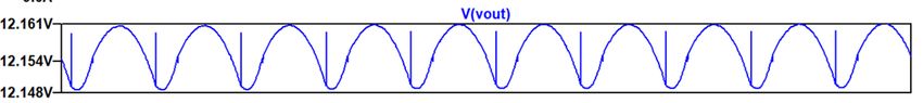
38                              M. CSIZMADIA, M. KUCZMANN

changes in current (di/dt) or voltage (du/dt) generate higher order harmonics and the
effect of parasitic inductances and capacities are not negligible. The next generation of
the semiconductor devices, like Silicon Carbide (SiC) or Gallium Nitride (GaN) gives
new opportunities the design of the SMPS and control circuits.

                    2. Operation and design of buck converter
    Buck converter is a type of non-isolated (Direct Current) DC/DC converters, which
steps down the input voltage [3]. The non-isolated buck converter contains two
semiconductors (transistor and diode) and energy storage elements (inductors and
capacitors). The function of these elements is dual: they store the energy and have filter
function. Nowadays, for the better efficiency the diodes are replaced by transistors
having the same function, but better properties. This type of buck converters is called
the synchronous buck converter in the literature [4].
    The basic operation of the buck converter can be illustrated by looking at the two
current paths represented by the states of the two switches (Fig. 1): SW1 is the high-
side switch and SW2 is the low side switch (diode). In the first period the high-side
switch is turned on and the energy flows from input - through the LC filter - to the
output. The energy in the inductor increases. In the second period high-side switch turn
off and the low-side switch turned on. The energy from the inductor flows to the output,
through SW2. Relevant, that at the same time just one semiconductor conducts; another
one is off-state. Between the state-change a dead time has to apply avoiding the short
circuit.

                                    Fig. 1. Buck converter

    In steady state, it can distinguish two operating mode, which depend on the current
in the energy storage element (inductor):
     •   Continuous Conduction Mode (CCM);
     •   Discontinuous Conduction Mode (DCM).
   In CCM the inductor current goes to zero in each switching period, in DCM the
inductor sits with no current and no stored energy for part of the time.
   The objective of this work is to design (and after that build up) a synchronous buck
converter in CCM, because in the practice this solution is more common. The circuit of

Pollack Periodica 15, 2020, 2

                                                                Unauthenticated | Downloaded 10/25/20 06:17 AM UTC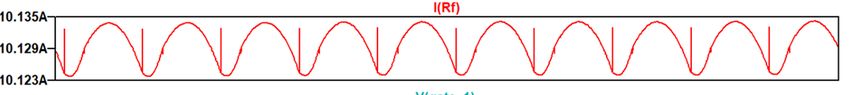
DESIGN OF LQR CONTROLLER FOR GAN BASED BUCK CONVERTER                                  39

buck converter is shown in Fig. 1. This modeling method takes the parasite resistance of
capacitor and inductor into consideration.
    In the example, the input voltage of the buck converter is 48 V, the output voltage is
12 V, the output power is 100 W, and the switching frequency is 1 MHz. The maximum
allowable ripple current is 10% of the maximal output current, and the value of the
voltage ripple is maximum 100 mV. Table I contains the additional parameters of the
converter.

                                            Table I
                The parameter values used in the simulation of the buck converter
                                Parameter                 Value
                                    d                      0.25
                                    L                    10 µH
                                    rL                  21.8 mΩ
                                    C                     10 µF
                                  ESR                    5.7 mΩ
                                    Rt                    1.2 Ω
                                    Ts                     1 µs

     In steady-state the duty cycle is very important, which gives the ratio between the on
time and the switching period and the ratio between outputs furthermore input voltage.
It is denoted by d, accordingly [4]:

     =     ,,                                                                                   (1)

where Vo is the output voltage and Vi is the input voltage of the converter. The value of
the output current can be calculated by using the output power and the output voltage:

      =    ,                                                                                    (2)

where Io is the output current and the Po is the output power of the converter.
    Inductors can be manufactured in various materials typically with a tolerance of
±20%. Inductors have an inherent DC resistance (rL), which impacts the performance of
the output stage. Minimizing the Direct Current Resistance (DCR) improves the overall
efficiency of the converter. There is a trade-off between inductance and ripple current:
the lower inductance causes higher ripple through the inductor, typically 10-30% of the
maximum output current. In this case the value of ripple current has been defined. The
value of the inductor can be calculated [4]:

     =              =
                        |   |
                                 ,                                                              (3)

where ∆IL is the ripple current through the inductor, ton is the on time of the
semiconductors and the toff is the off time of semiconductor.

                                                                   Pollack Periodica 15, 2020, 2

                                                                                    Unauthenticated | Downloaded 10/25/20 06:17 AM UTC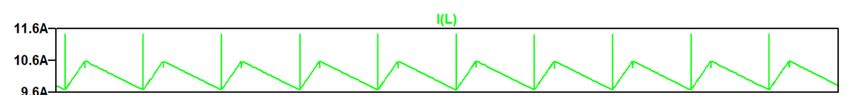
40                                          M. CSIZMADIA, M. KUCZMANN

    The output capacitor COUT maintains the regulated output voltage during the times
when the inductor current is higher or lower than the output current, therefore the role of
this part is very important. Each capacitor has an Equivalent Serial Resistance (ESR),
which comes from the physical design. This parameter is very important in case of the
design of regulators, because it influences the response time of the feedback loop and is
also one component of the output voltage ripple. Choosing of the value of the capacitor
requires great care. The minimal value of the capacitor can be calculated as [4]:

             =
                                        ∆       !"
                                                       ,                                                  (4)

where fsw is the switching frequency and ∆Voutmax is the output voltage ripple through the
output capacitor.

                                                 3. State-space equations
    There are lots of modeling methods, which describe the behavior of the system e.g.
the DQ-form [5], the state-space equations. The method of state-space describes the
system with the state variables, which can be the voltage across the capacitor and the
current through the inductor. These equations are first-order differential equations. In
case of switching converters, these equations should be linearized, so they approximate
the switching converter as a continuous linear system. In case of linear, causal and
invariant Single-Input Single Output (SISO) system the state-space model can be
descried by [6]:

         $
               = %$             + '(        ,

     *       = +, $         ,                                                                             (5)

where x(t) is the state vector; s(t) is the input; y(t) is the output; A is the system matrix;
b is the input vector; CT is the output vector.
    The system matrix A is NxN-order quadratic matrix.
    According to Kirchhoff's law, the following equations can be written [7]:

     -. + /                     = 4 = 53 678 −                   :,
                       012                                 012
                 !"    03                                  03
                                                                                                          (6)

and

     /8 78 +           = 4 − 4 = 4 − 53 678 −                               :.
                  0                                                   012
                  03                                                  03
                                                                                                          (7)

The of output voltage is the following:

     4 =             7       +                  -. .
              " ;                "
             " ?; 8           " ?;
                                                                                                          (8)

Pollack Periodica 15, 2020, 2

                                                                                 Unauthenticated | Downloaded 10/25/20 06:17 AM UTC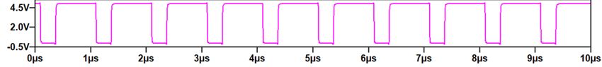
DESIGN OF LQR CONTROLLER FOR GAN BASED BUCK CONVERTER                                   41

When SW1 is turned on (and SW2 is turned off), conducts for a ratio d of a period. The
state matrix at the state ton is, from (6), (7) and (8):

       78      5 / + / !" /8 + /           !" 53           53
             D− 3 8                                −                   H           1
   @    A = CC
                     53 + / !"                          53 + /    !"   G I 78 J + K M 4 ,
     -.                53                                  1           G -.
             C                                     −                   G           0
             B      53 + / !"                           53 + /    !"   F
          = % $ + ' (,

                                     78      0
   4 = N"                       OI      J + N O 4 = + , $.
             " ;       "
              ?;   " ?;        -.      0
                                                                                                   (9)

When SW1 is turned off, SW2 conducts for a ratio of (1-d) of a period. The state space
equation can be written as (toff state matrix):

       78      5 / + / !" /8 + /           !" 53           53
             D− 3 8                                −                   H
   @    A = CC
                     53 + / !"                          53 + /    !"   G I 78 J + N0O 4
     -.                53                                  1           G -.        0
             C                                     −                   G
             B      53 + / !"                           53 + /    !"   F
          = % $ + ' (,

                                     78      0
   4 = N"                       OI      J + N O 4 = 4 + , $.
             " ;       "
              ?;   " ?;        -.      0
                                                                                                  (10)

Averaging the state-variable description [3]:

            = 6%      +%        1−       : $ + 6'       +'        1−       : (,
   0Q 3
    03
                                                                                                  (11)

   *        = 6+ ,    + +,     1−       : $.                                                      (12)

Separating the variables:

       = R + S,                                                                                   (13)

   $ = T + $U,                                                                                    (14)

the uppercase letters. For example, Q V is a small-signal variation in the DC or steady-
where small signal values are represented with a tilde and the steady state component by

state component X.
    The small signal state space description:

            = %$U + W %       −%       T+ '        −'    4 X S,
    V 3
   0Q
    03
                                                                                                  (15)

   -U = + , $U + W+ , − + , X T S .                                                               (16)

                                                                        Pollack Periodica 15, 2020, 2

                                                                                       Unauthenticated | Downloaded 10/25/20 06:17 AM UTC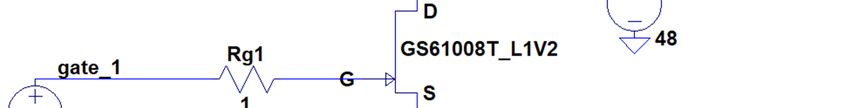
42                                   M. CSIZMADIA, M. KUCZMANN

The linearized and simplified model of the buck converter can be written as

                    −                              −
      0                 " ; ?; ; ?; "               "
                                                                        78      0
     Y01   Z   =Y                                                  ZI      J + \8 ] 4 .
       03                   8 " ?;                  . " ?;
         2                     "
                                                   −
                                                           [            -.      0
                                                                                                           (17)
       03                   . " ?;                  . " ?;

Substituting the values of Table I it results in

               −2747.3        −99527.2         25000
     %=N                               O , '=N       O .
               99527.2        −82939.4           0
                                                                                                           (18)

The transfer function of the system can be obtained, i.e.

     e ( =                                     .
                        [f[. g?h.f   ⋅[jk
                 g l ? .mno⋅[jp g?[.j[q⋅[jrs
                                                                                                           (19)

    The step response of the system without compensator between input and output
voltage is shown in Fig. 2.

                            Fig. 2. Step response of the system without compensator

                                4. Linear quadratic regulator design

    For regulatory purposes the Linear Quadratic Regulator (LQR) has been used. LQR
is an optimal control, and type of a state feedback, which guarantees at least 60° phase
margin [8]. It can be used in case of SISO or Multiple-Input Multiple-Output (MIMO)
system. For LQR design it is necessary the use the state space variable description (5).
In addition, a functional with linear quadratic form can be defined by the general form:

     t $, u = vj w$ , x$ + u, yuz
                    [   ,
             h
                                                   ,                                                       (20)

where Q and R are the weighting matrices, Q ≥ 0, and R > 0 . The aim of an LQR
strategy is to minimize the functional J. Because the aim is searching the minimum
value of this functional, also the LQR gives the optimum value of control u.

Pollack Periodica 15, 2020, 2

                                                                                    Unauthenticated | Downloaded 10/25/20 06:17 AM UTC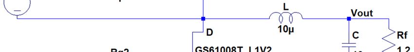
DESIGN OF LQR CONTROLLER FOR GAN BASED BUCK CONVERTER                                       43

    It is very common, that the LQR system is augmented with an extra integrator [8],
[9]: the derivative of this state is error, which is the difference between the output and
the reference voltage. The modified block diagram of the closed loop system is shown
in Fig. 3.

                                       Fig. 3. LQR system with integrator

   According to Fig. 3 the new state space matrices of the system can be describing
[10] [11], [12].

         {$U + |
        =%     {uV , * = +} , $U,
   0Q
   03
                                                                                                    (21)

where

   { = N %•            ~         S = N'O ,       +} , = N+ O.
                                                          ,
   %                     O       '
        −+             ~              ~                  ~
                                                                                                    (22)

    It is the designer’s job to find the values of Q and the value of R. There exist a lot of
solutions and algorithms for this problem, which prefer different parameters of the
system. To determine Q and R the energy-based design method have been used, which
is described in [12] and [13]. The buck converter extended with an integrator is a third-

controller can regulate just the duty cycle ( S ). Accordingly, the matrices have been set
order system therefore the matrices Q is a 3 by 3 matrix. R’s dimension is 1 because the

to be:

              8
                  h
                           0           0
    x=Y 0                  €.h         0 Z , y = 1.
        0                  0         ⋅ 10[j
                                                                                                    (23)

                                                S ,Q,R) a function by Matlab the
                                             { ,'
Solving the LQR problem with [k, P, e] = lqr(%
results is:

    • = w‚[           ‚h     ‚ z = w2        1    20833z.                                           (24)

                                                                            Pollack Periodica 15, 2020, 2

                                                                                         Unauthenticated | Downloaded 10/25/20 06:17 AM UTC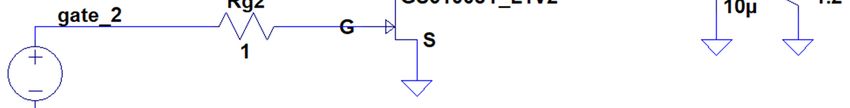
44                              M. CSIZMADIA, M. KUCZMANN

                                   5. Simulation results
   The controller has also been tested in the frame of Matlab Simulink. The
implementation of Buck converter is shown in Fig. 4, and the closed loop system with
LQR controller is shown in Fig. 5 [14].

                        Fig. 4. Simulink Block model of Buck converter

                      Fig. 5. Simulink model of controlled Buck converter

   The converter is also tested with load disturbances: in t=1.2 ms the load resistance is
changed to 1.09 Ω (10% higher output current), and t=2 ms the output resistance and

Pollack Periodica 15, 2020, 2

                                                                    Unauthenticated | Downloaded 10/25/20 06:17 AM UTC
DESIGN OF LQR CONTROLLER FOR GAN BASED BUCK CONVERTER 45
current are changed back to normal, 1.2 Ω. In Fig. 6, the first plot shows the output
resistance, the second is the output voltage and the third is the output current. The
voltage overshoot, in case of 1 A overcurrent, is about 660 mV, and after 66 ms the
output is stabilized.
Fig. 6. Dynamic test of Buck converter
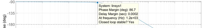
The Bode plot of the open loop system it shown in Fig. 7. The correct operation of
the controller can be checked with the enough phase margins: in this case it is 86.7°.
Fig. 7. Bode plot of Buck converter
Pollack Periodica 15, 2020, 2
Unauthenticated | Downloaded 10/25/20 06:17 AM UTC
46                              M. CSIZMADIA, M. KUCZMANN

    The open loop simulation results in LTSpice with semiconductor GaN E-HEMT
(GS61008T) is shown in Fig. 8. The GaN based power electronics system can be
exceeding the Si-system limits: reduce the energy cost, it is works on higher switching
frequency (or on the same frequency it has lower loss) and it has better thermal and
electrical properties [15]. To achieve good switching properties, separated turn-on and
turn-off gate resistors are used. The turn on resistor is selected 10 Ω and the off resistor
is 1 Ω. The dead time between the high and low side signal is 25 ns [16]. Table II
contains the important simulation results and in Fig. 9 the following simulation results
are presented: the first plot shows the inductor current, the second plot shows the output
voltage, the third plot shows the output current, the fourth plot shows the high side gate
drive signal and the fifth plot shows the low side gate drive signal.

                  Fig. 8. Buck converter open loop circuit diagram in LTSpice

                                            Table II
                                Buck converter simulation results
                              Parameter                   Value
                                   D                       0.25
                                    L                     10 µH
                                   rL                    5.4 mΩ
                                   C                      10 µF
                                  ESR                    5.7 mΩ
                                   Rt                     1.2 Ω
                                   Ts                      1 µs
                                 Ploss T1               4.153 W
                                 Ploss T2              746.45 mW
                            Total Efficiency             97.58%

Pollack Periodica 15, 2020, 2

                                                                    Unauthenticated | Downloaded 10/25/20 06:17 AM UTC
DESIGN OF LQR CONTROLLER FOR GAN BASED BUCK CONVERTER 47
The role of electromagnetic compatibility (EMC) is very important in the design
processes of SMPS especially for high frequency applications. Therefore, measuring
this parameter is necessary in case of SMPS [17].
Fig. 9. LTSpice simulation results in steady state
6. Conclusion
A linear quadratic regulator controller has been designed for the Buck converter,
which is based on the state feedback. The controller has been tested via Matlab and
LTSpice. It is shown that this robust regulator can be realized easily. Next the circuit
will be designed with GaN E-HEMT semiconductor and high frequency gate driver
from Texas Instruments. The controller circuit will be designed in two ways: realized by
passive components like operational amplifier, resistor and capacitor, and by digital
controller.
Open Access statement
This is an open-access article distributed under the terms of the Creative Commons
Attribution 4.0 International License (https://creativecommons.org/licenses/by/4.0/),
which permits unrestricted use, distribution, and reproduction in any medium, provided
the original author and source are credited, a link to the CC License is provided, and
changes - if any - are indicated. (SID_1)
Pollack Periodica 15, 2020, 2
Unauthenticated | Downloaded 10/25/20 06:17 AM UTC48 M. CSIZMADIA, M. KUCZMANN
References
[1] Hopkins A., McNeill N., Drury W. D., Atkins A. Deploying SiC BJTs in an 800-V
switched-mode power supply for hybrid & electric vehicles, 2017 IEEE 26th International
Symposium on Industrial Electronics, Edinburgh, UK, 19-21 June 2017, pp. 1430‒1438.
[2] Maharjan M., Tandukar P., Bjracharya A., dos Reis F. B., Tamrakar U., Shrestha D., dos
Reis F. S., Tonkoski R. SEPIC converter with wide bandgap semiconductor for PV battery
charger, Brazilian Power Electronics Conference, Juiz de Fora, Brazil, 19-22 November
2017, 2018, pp. 481‒486.
[3] Mohan N., Undeland T. M., Robbins W. P. Power electronics; converters, applications,
and design, Wiley, 1995.
[4] Lee J. Basic calculation of a Buck converter’s power stage, Richtek Application Note,
AN041, 2015.
[5] Kelemen A., Kutasi N. Induction-heating voltage inverter with hybrid LLC resonant load,
the D-Q model, Pollack Periodica, Vol. 2, No. 2, 2007, pp. 27‒37.
[6] Kuczmann M. Signal and Systems (in Hungarian), Universitas, Győr, Hungary, 2005.
[7] Ahmed S. R., Noor N. J., Mostafa S. State space modeling of a Buck converter and design a
controller, BSc Thesis, Brac University, Bangladesh, 2017.
[8] Rytkonen F. J., Tymerski R. Modern control regulator design for dc-dc converters,
Portland State University, Electrical and Computer Engineering Department, 2005,
pages 57.
[9] Keviczky L., Bars R., Hetthéssy J., Bányász C. Control engineering, Széchenyi István
University, Hungary, 2011.
[10] Ogata K. Modern control engineering, Prentice Hall, 2009.
[11] Lindiya S. A., Vijayarekha K., Palani S., Determistic LQR controller for DC/DC Buck
converter, Biennial International Conference of Power and Energy Systems: Towards
Sustainable Energy, Bangalore, India, 21-23 January 2016, pp. 428‒433.
[12] Stumpf P., Peschka A., Kurucsó B. Design of a quadratic boost converter, National
Scientific Student’s Associaton, Budapest, Hungary, 25-27 Marc 2015, pp. 25‒28.
[13] Arango E., Ramos-Paja C. A., Calvente J., Giral R., Serena S. Asymmetrical interlaved
DC/DC switching converters for photovoltaic and fuel cell applications, Part 1, Circuit
generation, analysis and design, Energies, Vol. 5, No. 11, 2012, pp. 4590–4623.
[14] Alkrunz M., Yazici I. Design of discrete time controllers for the DC-DC boost converter,
Sakarya Üniveristesi Fen Bilimeri Enstitüsü Dergisi Sakarya University Journal of Science,
2016, pp. 75‒82.
[15] Csizmadia M. and Kuczmann M., Power Semiconductor Trends in Electric Drive Systems,
Acta Technica Jaurinensis, Vol. 12, No. 1, pp. 13‒25.
[16] Gan Systems, Design with GaN enhancement mode HEMT, Application Guide.
[17] Istók R., Kádár P. EMC measurement systems and noise suppression methods for LED laps
and RF lighting controls, Pollack Periodica, Vol. 11, No. 3, 2016, pp. 141‒152.
Pollack Periodica 15, 2020, 2
Unauthenticated | Downloaded 10/25/20 06:17 AM UTCYou can also read