Application Note SPWM Generator for Inverter Design - Dialog Semiconductor
←
→
Page content transcription
If your browser does not render page correctly, please read the page content below
Application Note
 SPWM Generator for Inverter
 Design
 AN-CM-302

Abstract
This app note implements a SPWM Generator. It describes the implemented logic, GreenPAK
implementation detail, and the results obtained.

This application note comes complete with design files which can be found in the References
section.
AN-CM-302
SPWM Generator for Inverter Design

Contents
Abstract ................................................................................................................................................ 1
Contents ............................................................................................................................................... 2
Figures .................................................................................................................................................. 2
Tables ................................................................................................................................................... 2
1 Terms and Definitions................................................................................................................... 3
2 References ..................................................................................................................................... 3
3 Introduction.................................................................................................................................... 4
4 SPWM Inverter Concept................................................................................................................ 5
5 SPWM Characteristics .................................................................................................................. 6
6 Implementation and Configuration of SPWM Generator ......................................................... 10
7 Tests and Conclusion ................................................................................................................. 15
Conclusion ......................................................................................................................................... 16
Revision History ................................................................................................................................ 17

Figures
Figure 1: Basic H-bridge circuit ............................................................................................................. 5
Figure 2: Basic PWM Control Signals and Output Voltage ................................................................... 6
Figure 3: Simplified Schemtica of Sinusoidal PWM Modulation............................................................ 6
Figure 4: Sinusoidal PWM Modulation and Output Signals .................................................................. 7
Figure 5: Over-modulated SPWM ......................................................................................................... 8
Figure 6: SPWM Block Diagram ............................................................................................................ 9
Figure 7: SPWM to H-Bridge Connection.............................................................................................. 9
Figure 8: Triangle Waveform Generator.............................................................................................. 10
Figure 9: CNT1 Configuration ............................................................................................................. 11
Figure 10: CNT2 Configuration ........................................................................................................... 11
Figure 11: CNT0 Configuration ........................................................................................................... 12
Figure 12: Odd Output Control ............................................................................................................ 13
Figure 13: Modulator Block Diagram ................................................................................................... 13
Figure 14: SPWM Generator Implementation ..................................................................................... 14
Figure 15: System Implementation...................................................................................................... 15
Figure 16: SPWM Output Voltage ....................................................................................................... 15
Figure 17: SPWM Output Signal ......................................................................................................... 16

Tables
Table 1: Logic of Switches..................................................................................................................... 5

Application Note Revision 1.0 13-Oct-2020

CFR0014 2 of 18 © 2021 Dialog Semiconductor
AN-CM-302
SPWM Generator for Inverter Design

1 Terms and Definitions
IC Integrated circuit
IR Infrared
LED Light-emitting diode

2 References
For related documents and software, please visit:
https://www.dialog-semiconductor.com/products/greenpak
Download our free GreenPAK Designer software [1] to open the .gp files [2] and view the proposed
circuit design. Use the GreenPAK development tools [3] to freeze the design into your own
customized IC in a matter of minutes. Dialog Semiconductor provides a complete library of
application notes [4] featuring design examples as well as explanations of features and blocks within
the Dialog IC.
[1] GreenPAK Designer Software, Software Download and User Guide, Dialog Semiconductor
[2] AN-CM-302 SPWM Generator.gp, GreenPAK Design File, Dialog Semiconductor
[3] GreenPAK Development Tools, GreenPAK Development Tools Webpage, Dialog
 Semiconductor
[4] GreenPAK Application Notes, GreenPAK Application Notes Webpage, Dialog Semiconductor
[5] AN-CM-265 Programmable Limits PWM, Application Note, Dialog Semiconductor.
[6] SLG46826V, Datasheet, Dialog Semiconductor.

Authors: Ing. Alberto I. Leibovich & PhD Ing. Pablo E. Leibovich
This article was originally published on EDN.

Application Note Revision 1.0 13-Oct-2020

CFR0014 3 of 18 © 2021 Dialog Semiconductor
AN-CM-302
SPWM Generator for Inverter Design

3 Introduction
Renewable energy continues to be a massive trend around the world. As methods for capturing wind,
solar and other forms of renewable energy have developed, the cost and efficiency of renewable
energy systems have become more appealing to both companies and consumers. In fact, in 2016,
the global monetary investment in renewable energy fell to the lowest number in years, while
simultaneously the record was broken for the largest number of renewable energy installations in a
given year. With the tradeoff in cost and development changing so greatly, the market for further
innovation is booming.
Amongst the components used for renewable energy resources an inverter stands out as a uniquely
critical system component. As most renewable energy is generated in DC, an inverter plays a key
role in converting the DC into AC for effective integration into existing power grids. In hybrid power
systems (combining different renewable resources) and micro-grid systems, the use of inverters is
essential.
Renewable energy inverters play a role in industrial applications where single-phase and three-phase
motors and other rotary machines are used. Variable frequency and voltage (obtained from an
inverter) is the principle of autonomous control in this type of equipment.
To implement the power conversion, DC-AC inverters usually apply the Pulse Width Modulation
(PWM) technique. PWM is a useful technique wherein switches like Power MOSFETs are controlled
with pulses of variable widths. In order to obtain an automatic control and regulation, the PWM
technique is used to maintain the AC voltage output of the inverter (and its frequency) at the nominal
value independent of the output load.
Many studies and technologies have been developed to obtain better response from the inverter
control system. Conventional inverters change the output voltage according to the changes in the
load. To reduce the sensitivity of the output voltage to load changes, PWM based inverters regulate
the output voltage by changing the width of the pulses generated at a comparatively high frequency.
As a result, the output voltage depends on the switching frequency and pulse width, which varies
according to the value of the load connected at the output. With this type of regulation, the inverters
provide a constant nominal voltage and a frequency independent of the output power.
Several methods of generating the pulse width modulation have been studied. The efficiency
parameters of an inverter, such as switching losses and harmonic reduction, are the main factors
considered in any modulation technique evaluation. Because of the analysis of several tests,
Sinusoidal pulse width modulation (SPWM) is widely used in power electronics as the modulation
method for PWM inverters.

Application Note Revision 1.0 13-Oct-2020

CFR0014 4 of 18 © 2021 Dialog Semiconductor
AN-CM-302
SPWM Generator for Inverter Design

4 SPWM Inverter Concept
A three-phase wave bridge inverter is the most used inverter topology in industrial applications. To
simplify the concept a single-phase version is analyzed. The single-phase design includes switching
transistors or IGBTs on each arm of the H-bridge with antiparallel freewheeling diodes to discharge
when the switch is turned off. Its schematic is shown in Figure 1.

 Figure 1: Basic H-bridge circuit

The transistors (usually power MOSFETs) are identified as S1, S2, S3 and S4. The switches are
alternated such that both transistors of the same arm are not conducting or opened simultaneously,
thereby preventing a short circuit.

To generate the alternating current in load, transistors operate in a pair (S1 and S2 conducting, S3
and S4 opened or vice versa). Table I shows the different switching stages and the applied voltage to
the load.

Table 1: Logic of Switches
 S1 S2 S3 S4 Vab
 ON ON OFF OFF +VDC
 OFF OFF ON ON -VDC

A square wave inverter (also known as Basic Inverter) is operated by two square waves in opposite
phase and with frequency equal to the desired frequency at the output. One of the waves is applied
to S1 and S2 and the other waveform to S3 and S4. Figure 2 shows the PWM control signals and the
obtained voltage in the load if this type of inverter is used.

Application Note Revision 1.0 13-Oct-2020

CFR0014 5 of 18 © 2021 Dialog Semiconductor
AN-CM-302
SPWM Generator for Inverter Design

 Figure 2: Basic PWM Control Signals and Output Voltage

PWM is based on the generation of constant amplitude pulses, with modulation of the pulse duration
by varying the duty cycle. The reference or modulated signal is the desired signal output (sinusoidal
in the case of voltage waveforms at the output of an inverter) and the carrier signal must have a
frequency much greater than the modulated one. This is the main reason for the usage of Sinusoidal
PWM (SPWM) as the modulation method for PWM inverters.

5 SPWM Characteristics
SPWM modulation is based on constant amplitude pulses with different duty cycles for each period.
The width of pulses is obtained by modulation of a carrier to obtain the desired output voltage and to
reduce its harmonic content.
The carrier signal of SPWM is usually a triangular wave with a high frequency, generally in several
KHz. The modulation signal of SPWM is a sinusoidal waveform with a frequency equal to the desired
output voltage frequency (50 or 60 Hz).
In Figure 3, a simplified schematic of sinusoidal modulation is shown. The switching signal is
generated by comparing the sinusoidal waveform and the triangular carrier waveform. The
comparator output is high when sinusoidal voltage is greater than the triangular voltage. The output
pulses of the comparator are used as the gate pulses of the H-Bridge presented in the previous
section.

 Figure 3: Simplified Schemtica of Sinusoidal PWM Modulation

In order to obtain better results, the frequency ratio between the triangular and the sinusoidal
waveforms must be an integer N = fC/fS, where fC is the carrier frequency (the triangular waveform)
and fS is the modulation frequency (the sine waveform). With this condition, the number of voltage
Application Note Revision 1.0 13-Oct-2020

CFR0014 6 of 18 © 2021 Dialog Semiconductor
AN-CM-302
SPWM Generator for Inverter Design

pulses per half-cycle results in N/2. This effect can be seen in Figure 4, where the triangular, sine
and the PWM output waveforms are shown.

 Figure 4: Sinusoidal PWM Modulation and Output Signals

If SPWM is analyzed mathematically, a modulation index m can be defined as the ratio between the
amplitude of the sine wave (VS) and the triangular wave (VC):
 ̂

 =
 ̂

For regulation range, m must be equal or less than 1.0. If the previous condition is considered, the
output voltage of the H-bridge controlled by SPWM results in:
 √2
 =
 4

Where VDC is the input DC voltage to the inverter.
The modulation process of duty cycle is designed for m equal to or less than one. If m is higher, there
will be periods of the triangle signal in which no intersection of the carrier and the modulation signal
will exist. The effect on the output signal is shown in figure 5. However, it’s important to note that a
certain amount of over-modulation is sometimes used with the aim of obtaining a higher AC voltage
amplitude.

Application Note Revision 1.0 13-Oct-2020

CFR0014 7 of 18 © 2021 Dialog Semiconductor
AN-CM-302
SPWM Generator for Inverter Design

 Figure 5: Over-modulated SPWM

If SPWM is analyzed in terms of waveform quality the harmonics must be considered. The SPWM
generates different harmonics of several orders in the voltage waveform. However, the dominant
ones are of order N and N±2 (where N was defined as fC/fS). If over-modulation is considered, the
output voltage has a higher harmonics content as a trade-off in generating a higher voltage. By
varying the sinusoidal voltage, the output voltage can be regulated.

These concepts of triangular waveform with fixed amplitude and frequency and sinusoidal waveform
with fixed frequency (equal to the output frequency) and variable amplitude are the basis of the
SPWM Generator implemented in this application note.
The SPWM Generator described and implemented in this app note is based on the block diagram
shown in Figure 6.

Application Note Revision 1.0 13-Oct-2020

CFR0014 8 of 18 © 2021 Dialog Semiconductor
AN-CM-302
SPWM Generator for Inverter Design

 Figure 6: SPWM Block Diagram

A high frequency triangular waveform is necessary to generate the SPWM signals. This task is
implemented with finite state machines (FSM)/Counters and D-type Flip Flops and is referenced as
HF Triangle Generator in the diagram. The generator is based on the AN-CM-265 Programmable
Limits PWM app note [1], generating a PWM with triangular variation of the duty cycle. As a
triangular waveform is required, a low-pass filter is applied to eliminate the very-high frequency of the
square wave.

This triangular waveform is compared with an external low voltage 50 or 60 Hz sine waveform with
the Analog Comparators of the GreenPAK. With this comparison, the sinusoidal modulation of the
PWM is implemented as described in the previous section. Finally, an inverter is used to generate
the complementary signals for the SPWM outputs.

 The output of the SPWM generator is connected to an H-Bridge as shown in Figure 7.

 Figure 7: SPWM to H-Bridge Connection

Application Note Revision 1.0 13-Oct-2020

CFR0014 9 of 18 © 2021 Dialog Semiconductor
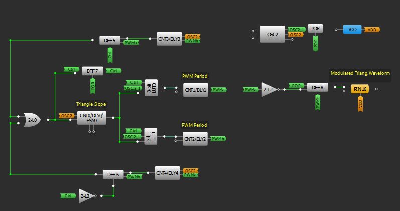
AN-CM-302
SPWM Generator for Inverter Design

As seen from Figure 7, SPWM output and its complementary signal are connected one to each
transistor of the same leg. The output of the H-Bridge contains an LC-filter so the high-frequency
component of the SPWM is filtered, and finally, the sinusoidal waveform of 50 or 60 Hz is applied to
the load.

6 Implementation and Configuration of SPWM Generator
The implementation of the SPWM Generator is based on a SLG46826V GreenPAK [2]. This
Programmable Mixed-Signal ASIC contains Finite State Machine/Digital Counters, High-speed
Analog Comparators and high-frequency Oscillators that can be used for generating the required
triangular waveform and the sinusoidal modulation.
The high frequency triangular waveform generator is based on the AN-CM-265 Programmable Limits
PWM app note [5] The implementation of the generator can be seen in Figure 8.

 Figure 8: Triangle Waveform Generator

The generator uses the internal 25 MHz oscillator, configured for an output frequency of 12.5 MHz.
This clock, combined with macrocells CNT1 and CNT2, generates the corresponding square
waveform with the desired duty cycle. The configuration of both counters can be seen in Figure 9 and
Figure 10.

Application Note Revision 1.0 13-Oct-2020

CFR0014 10 of 18 © 2021 Dialog Semiconductor
AN-CM-302
SPWM Generator for Inverter Design

 Figure 9: CNT1 Configuration Figure 10: CNT2 Configuration

Counter data of both counters is defined to generate a PWM of 50 KHz by applying the expression:
 12.5
 = = = 50
 1 + 1 249 + 1

Relative phase of counters is varied by CNT0/DLY0/FSM0. The slope of triangular duty cycle
variation is configured by setting CNT0 counter data following the equation:
 1 +1 250
 = ( 0 + 1) = (24 + 1) ∗ = 500
 12.5

Application Note Revision 1.0 13-Oct-2020

CFR0014 11 of 18 © 2021 Dialog Semiconductor
AN-CM-302
SPWM Generator for Inverter Design

 Figure 11: CNT0 Configuration

With this configuration the triangular waveform has a period of 1 ms, so a 1 KHz triangular waveform
is obtained. In this design a 50 Hz SPWM inverter is implemented but can be modified for 60 Hz or
other frequencies by changing the period of the triangular waveform.

The high frequency PWM with triangular variation is connected to PIN 16, where the corresponding,
external low pass filter is connected. This filter is based on a first-order RC filter, with a 1.5 kΩ
resistor and a 10 nF capacitor so the cut-off frequency of the filter results 10.6 KHz.

The output of the filter, as shown in the block diagram of Figure 6, is connected to the High-speed
Analog Comparator ACMP0H. The Configuration of ACMP0H is shown in Figure 12.

Application Note Revision 1.0 13-Oct-2020

CFR0014 12 of 18 © 2021 Dialog Semiconductor
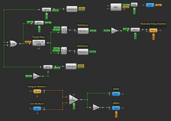
AN-CM-302
SPWM Generator for Inverter Design

 Figure 12: Odd Output Control

This block is used to compare voltage between PIN 20 and PIN 3. For best performance, the
hysteresis and the bandwidth limit options must be disabled. Thus, a low voltage sinusoidal
waveform generator must be connected to PIN 3 so the sinusoidal PWM modulation is obtained, as
shown in Figure 13.

 Figure 13: Modulator Block Diagram

In order to generate the complementary signals for PWM output, the 3-L1 look-up table is configured
as a logical inverter.

Finally, PWM outputs are connected to Pins 5 and 6.

As Pins 8 and 9 are connected to the I2C module of the GreenPAK IC, it’s necessary to connect
them with a pull-up resistor to VDD.

The entire SPWM implementation diagram is shown in Figure 14.

Application Note Revision 1.0 13-Oct-2020

CFR0014 13 of 18 © 2021 Dialog Semiconductor
AN-CM-302
SPWM Generator for Inverter Design

 Figure 14: SPWM Generator Implementation

Application Note Revision 1.0 13-Oct-2020

CFR0014 14 of 18 © 2021 Dialog Semiconductor
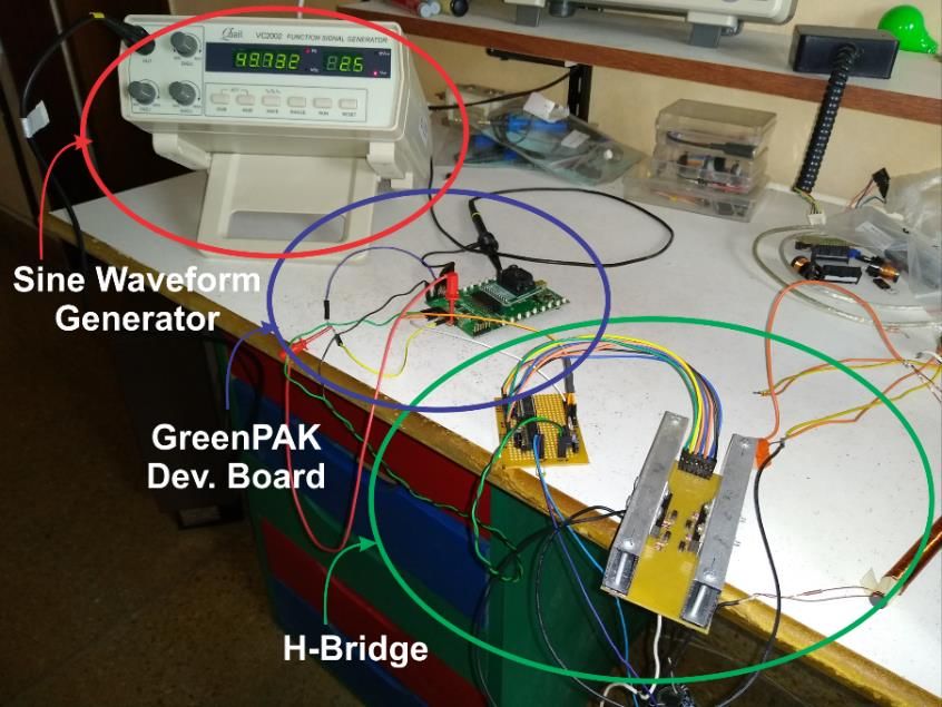
AN-CM-302
SPWM Generator for Inverter Design

7 Tests and Conclusion

To test the implementation, the entire system was assembled and analyzed with an oscilloscope.
The 50Hz sine wave signal was generated with a function signal generator, with a corresponding
amplitude and offset such that it can be connected directly to the SLG46826V. The entire system can
be seen in figure 15.

 Figure 15: System Implementation

To analyze the results, the voltage waveform at the load and the output signal on pin 5 of the
SLG46826V were logged.

In Figure 16, the output voltage applied to the load is shown. It can be seen that the output voltage
has a sinusoidal shape if measured after the LC Filter.

 Figure 16: SPWM Output Voltage

In Figure 17, the SPWM output signal at pin 5 of the SLG46826V is illustrated. It shows how the
output modifies its duty cycle with a sinusoidal variation.
Application Note Revision 1.0 13-Oct-2020

CFR0014 15 of 18 © 2021 Dialog Semiconductor
AN-CM-302
SPWM Generator for Inverter Design

 Figure 17: SPWM Output Signal

Conclusion
In this application note we implemented a Sinusoidal Pulse Width Modulation Generator. Sinusoidal
pulse width modulation (SPWM) is one of the most widely used methods for implementing power
inverters, useful for different applications such as motor controls and renewable energy applications.

There are several methods of implementing SPWM. In this application note, one of the simplest and
most used methods is shown. Each step of SPWM generation and how it can be connected and
filtered at the output is described.

The size of the entire measurement system is smaller than many other implementations and outlines
where GreenPAK can be used and replace other programmable devices, such as a microcontroller
or discrete circuitry.

Application Note Revision 1.0 13-Oct-2020

CFR0014 16 of 18 © 2021 Dialog Semiconductor
AN-CM-302
SPWM Generator for Inverter Design

Revision History
 Revision Date Description
 1.0 13-Oct-2020 Initial Version

Application Note Revision 1.0 13-Oct-2020

CFR0014 17 of 18 © 2021 Dialog Semiconductor
AN-CM-302
SPWM Generator for Inverter Design

Status Definitions

 Status Definition

 The content of this document is under review and subject to formal approval, which may result in modifications or
 DRAFT
 additions.
 APPROVED
 The content of this document has been approved for publication.
 or unmarked

Disclaimer
Information in this document is believed to be accurate and reliable. However, Dialog Semiconductor does not give any representations or
warranties, expressed or implied, as to the accuracy or completeness of such information. Dialog Semiconductor furthermore takes no
responsibility whatsoever for the content in this document if provided by any information source outside of Dialog Semiconductor.
Dialog Semiconductor reserves the right to change without notice the information published in this document, including without limitation the
specification and the design of the related semiconductor products, software and applications.

Applications, software, and semiconductor products described in this document are for illustrative purposes only. Dialog Semiconductor makes
no representation or warranty that such applications, software and semiconductor products will be suitable for the specified use without further
testing or modification. Unless otherwise agreed in writing, such testing or modification is the sole responsibility of the customer and Dialog
Semiconductor excludes all liability in this respect.
Customer notes that nothing in this document may be construed as a license for customer to use the Dialog Semiconductor products, software
and applications referred to in this document. Such license must be separately sought by customer with Dialog Semiconductor.

All use of Dialog Semiconductor products, software and applications referred to in this document are subject to Dialog Semiconductor’s Standard
Terms and Conditions of Sale, available on the company website (www.dialog-semiconductor.com) unless otherwise stated.

Dialog and the Dialog logo are trademarks of Dialog Semiconductor plc or its subsidiaries. All other product or service names are the property of
their respective owners.

© 2021 Dialog Semiconductor. All rights reserved.

Contacting Dialog Semiconductor
United Kingdom (Headquarters) North America Hong Kong China (Shenzhen)
Dialog Semiconductor (UK) LTD Dialog Semiconductor Inc. Dialog Semiconductor Hong Kong Dialog Semiconductor China
Phone: +44 1793 757700 Phone: +1 408 845 8500 Phone: +852 2607 4271 Phone: +86 755 2981 3669
Germany Japan Korea China (Shanghai)
Dialog Semiconductor GmbH Dialog Semiconductor K. K. Dialog Semiconductor Korea Dialog Semiconductor China
Phone: +49 7021 805-0 Phone: +81 3 5769 5100 Phone: +82 2 3469 8200 Phone: +86 21 5424 9058
The Netherlands Taiwan
Dialog Semiconductor B.V. Dialog Semiconductor Taiwan
Phone: +31 73 640 8822 Phone: +886 281 786 222
Email: Web site:
enquiry@diasemi.com www.dialog-semiconductor.com

Application Note Revision 1.0 13-Oct-2020

CFR0014 18 of 18 © 2021 Dialog Semiconductor
You can also read