SOA in High Power Semiconductors
←
→
Page content transcription
If your browser does not render page correctly, please read the page content below
SOA in High Power Semiconductors
                                      Alper Akdag

                        IAS, October 2006, Tampa, USA

Copyright © [2006] IEEE. Reprinted from the Industry Applications Society.

This material is posted here with permission of the IEEE. Such permission of the
IEEE does not in any way imply IEEE endorsement of any of ABB Switzerland Ltd,
Semiconductors's products or services. Internal or personal use of this material is
permitted. However, permission to reprint/republish this material for advertising or
promotional purposes or for creating new collective works for resale or redistribution
must be obtained from the IEEE by writing to pubs-permissions@ieee.org.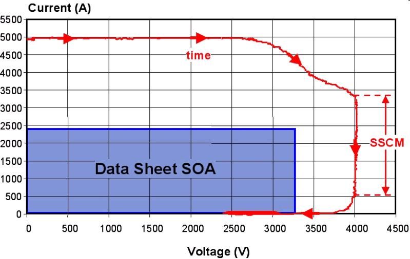
ABB Switzerland Ltd.                                                                           SOA in High Power Semiconductors

                     SOA in High Power Semiconductors
                                                            Alper Akdag
                                                        ABB Switzerland Ltd.
                                                           Semiconductors
                                                        Lenzburg, Switzerland

Abstract — This paper gives an overview on the SOA of high
power semiconductors. Two main types of high power
semiconductors are investigated: large area devices and modules
with paralleled chips. The paper explains the limits of SOA and
ways of improving it in the semiconductor design level, as well as
it gives practical advantages for a high SOA in the device.

   Keywords-component; Safe Operating Area; SOA; IGBT;
IGCT; high power semiconductor

                       I.    INTRODUCTION
    One of the main challenges today in the design of high
voltage – high power semiconductors is the Safe Operating
Area “SOA” capability [1]. A destruction point characterizes
the SOA limits whereas failures are largely related to the
                                                                                         Figure 1. Evolution of SOA
device design and/or process. In recent years, the SOA
performance for medium to low voltage devices has improved
immensely. Optimized emitter cell designs, the introduction of       Improved SOA performance will have a positive impact on
the NPT and SPT vertical design concepts in IGBTs and better-            i. manufacturability,
controlled lifetime reduction techniques have all helped in this        ii. reliability,
direction. However, previous experience and literature has             iii. power handling capability,
clearly pointed out that the SOA performance for higher                iv. ease of paralleling,
voltage devices rated above 2000V degrades significantly                v. better controllability,
when compared to the low to medium voltage class devices.              vi. better system and gate drive designs aimed at reducing
This downtrend is due to physical constraints in high voltage               the total system losses, and
structures and the high stress operating conditions.                  vii. employing more optimised protection schemes.
Furthermore, the trade-off between the optimisation of the
overall losses and the SOA capability has imposed further
restrictions in the design window of high voltage                          In order to ensure that high voltage devices do not exceed
semiconductors.                                                      their SOA limits, many restrictions were introduced for
                                                                     operating such devices. Therefore, system designers have
   The paper is structured as two parts. First part will             resolved into setting many circuit and gate drive parameters
investigate the SOA in large area devices (eg. GCT, GTO, etc.)       accordingly. Such modifications include an increase in gate
and the second part focuses on the IGBT modules which                resistance and the inclusion of protective active clamps or
consist of paralleled chips.                                         snubbers. This added complexity has had normally a negative
                                                                     impact on the performance, cost and size of high power
                      II.   TRENDS IN SOA                            electronic systems.
     Trends for the development of power semiconductors                    In order to overcome these problems, larger SOAs are
aimed for wide SOA limits are fuelled by many requirements           always favorable by the system designers and applications
in applications operating under hard-switching conditions.           engineers and for that reason semiconductor manufacturers
Evolution of SOA for an improved safe operating area is              have always felt the pressure for designing better SOA
demonstrated in Fig. 1.                                              performance devices. The new limits are reached by
                                                                     introducing new technologies in the power semiconductor
                                                                     designs as shown in Fig. 2.

IAS                                                 Page 1 of 5                                                Tampa, October 2006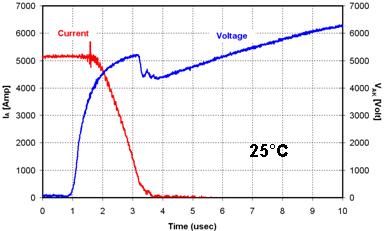
ABB Switzerland Ltd.                                                                                   SOA in High Power Semiconductors

           I
                   Pushing the RBSOA Limits

                   Device Capability
 n x Inom
                   New Limits
 2 x Inom
                                                                                                        GU
                 State-Of-The-Art Limits
                                                               V
                                                                         Figure 3. Principal of IGCT operation as parallel connected thyristor cells
                                              Vrated VSSCM                                        with an attached gate unit

   Figure 2. Extending the RBSOA limits of HV Power Semiconductors
                                                                           Based on these findings, the improvement of the SOA
                                                                       performance was carried out in three steps: cell optimization
          III.   INCREASED SOA IN LARGE AREA DEVICES                   (local SOA), lateral optimization of large area devices and a
                                                                       combination of local and lateral optimization techniques.
                       - A CASE FOR IGCT-
                                                                       A. Cell Optimization
    Previous experience and data have shown that the SOA of
high voltage devices up to 6500V degrades due to the physical              The improvement of the cell design by optimizing doping
stresses at very high voltage. Although improvements in SOA            profiles resulted in a maximum switching power density of
have been achieved, the turn-off capability of large area IGCT         1.5MW/cm2 for snubberless operation even when scaling up
devices is still the main parameter limiting higher system             the clamp stray inductance to 9.1μH for a device with 1.5cm2
ratings, especially at low temperatures.                               active area (Fig. 4). Here the ‘Switching-Self-Clamping-Mode’
                                                                       (SSCM) could be seen for the IGCT when switched against a
    The IGCT consists of a large number of parallel-operated           high DC-voltage and high clamp stray inductance. The SSCM
thyristor cells (Fig. 3) driven by a single gate unit. SOA             phenomena will be explained in the next section in detail.
performance can be limited by the following factors:
     i.    ruggedness of the individual cell                           B. Lateral Optimization of Large Area Devices
    ii.    current sharing effects due to heavy paralleling of the         A large area IGCT’s SOA was found to be significantly
           cells [2]                                                   below the switching power density of small devices.
   iii.    performance of the gate-driver [3, 4].                      Therefore, it must be concluded that a current redistribution
                                                                       during device turn-off is taking place. The major observation
    Analysis of the SOA limits for large area IGCTs has led to         that failure locations are remotely located from the gate contact
the following observations:                                            leads to the logical conclusion that the current redistributes into
                                                                       these remote areas during turn-off. Tailoring the current
   •      a larger active area of an IGCT always results in a          density distribution during the on-state phase by means of local
          lower average switching power density, even when             charge carrier lifetime control will reduce the effects of the
          accounting for the scaling of the switching circuit,         areas that are limiting the SOA performance of an IGCT. By
   •      an increase by a factor of 10 in active area only leads to   irradiating the device in remote areas from the gate with a
          an increase in turn-off current capability of a factor of    higher electron dose, the local charge charier lifetime is
          four,                                                        decreased. By gradually increasing the additional irradiation
                                                                       dose in remote areas, the current turn-off capability increases
   •      the SOA limit of a large area IGCT is typically reached
                                                                       until an optimum level is reached.
          while still operating in the macroscopic hard switching
          regime (i.e. the current commutation from cathode to
                                                                       C. Combined Local and Lateral Improvement
          gate is completed before the anode voltage starts to
          rise),                                                           These two combinations were proven to have a linear
   •      SOA failures are typically found in areas remote from        increase in turn-off capability. An increase of SOA of more
          the gate contact.                                            than 30% at RT (Fig. 5) was observed.

IAS                                                    Page 2 of 5                                                        Tampa, October 2006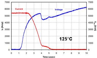
ABB Switzerland Ltd. SOA in High Power Semiconductors
1000 5000 device failure. Protection of the N+ source region is vital for
increasing the cell latch-up immunity of IGBTs.
800 4000 Diodes are also limited in their SOA due to dynamic
avalanche during reverse recovery. Under the adverse
600 3000
combination of high commutating di/dt, high current densities
V AK [V]
and high temperatures, the diode is forced during reverse
IA [A]
Switching Self Clamping Mode
recovery into dynamic avalanche. Extra carriers are then
400 2000 generated that are sensitive to any non-uniformities in the
device structure leading to destructive current filaments
forming in the device. Optimisation of the diode termination
200 1000 design, process and lifetime control has reduced the risk of
filaments occurring during dynamic avalanche resulting in
0 0 stable reverse recovery performance [5].
0 2 4 6 8 10
B. SOA Improvement Techniques
time [µ s]
For high voltage devices with typical low background
Figure 4. Turn-off characteristic of locally optimized Ø38mm reverse doping concentrations, the removal of the electron-hole plasma
conducting IGCT
during device turn-off forces the device into a strong dynamic
avalanche mode at much lower currents when compared to
lower voltage devices. Therefore, limiting substantially the
SOA performance of high voltage IGBTs and diodes. We will
6.5
show in this paper that all typical dynamic avalanche failure
not optimized
modes caused by the removal of the electron-hole plasma can
6.0 local optimized
be eliminated. Thereafter, this has led to the device
Ioff last pass @ 2.8kV [kA]
lateral optimized
experiencing a self-clamp avalanche mode during turn-off
5.5 local and lateral optimized
similar to that obtained in a standard unclamped inductive test.
We refer to this as the Switching Self-Clamping Mode
5.0 (SSCM), where the device overshoot voltage reaches a value
VSSCM close to the static breakdown voltage of the device as
4.5 shown in Fig. 6.
> 30% SOA improvement
As the voltage rises, the IGBT goes into dynamic avalanche
4.0
immediately after the MOS channel seizes to inject electrons
into the n-base region. The lack of electron compensation for
3.5
the recovering holes will modify the effective background
0 20 40 60 80 100 120 140
doping and electric field distribution characterised by the lower
Tj [°C] dv/dt value during dynamic avalanche. Unless device failure
occurs, the dynamic avalanche phase continues until the
Figure 5. SOA limits (last pass currents for snubberless turn-off at remaining electron-hole plasma is used up and subsequently
VD=2.8kV, Lσ = 0.3μH) for different junction temperatures and design dynamic avalanche is suddenly eliminated. Because of the
variations of ∅ 91mm, 4.5kV, asymmetric GCTs stray inductance in the commutation circuit, the voltage over
the IGBT starts to rise and eventually reaches the breakdown
voltage of the pn-junction, whereas avalanche-generated
IV. INCREASED SOA IN DEVICES WITH PARALLELED CHIPS carriers will carry the reverse current in the IGBT. Optimum
design of the device buffer region by employing a Soft-Punch-
- A CASE FOR IGBT- Through SPT concept will enable the device to withstand such
conditions by self-clamping the overshoot voltage successfully.
In this section, the SOA considerations and improvement Thus, leading to an ultimate square SOA capability up to the
techniques in the device level for an IGBT and diode will be device blocking voltage.
explained.
C. New HV-IGBT design platform
A. Failure mechanisms in IGBT and Diode
Dynamic cell latch-up represents the main failure mode The new technology was developed mainly for increasing
substantially the cell latch-up immunity for a wide SOA
when the IGBT turns off especially under extreme dynamic
performance. The main approach was to carefully optimise the
avalanche conditions. These conditions include high current,
IGBT cell pn junction profile while on the other hand, increase
high voltage, high temperature, large inductance and low gate
the protection level of the N+ source region especially at the
resistance values. Failures normally occur when the IGBT N+
weakest point near the MOS channel.
source injects enough electrons into the P channel region to
cause uncontrolled parasitic thyristor triggering leading to
IAS Page 3 of 5 Tampa, October 2006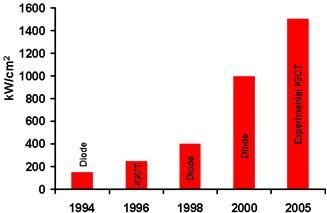
ABB Switzerland Ltd. SOA in High Power Semiconductors
MOS Channel On MOS Channel Off IGBT Off
Dynamic Avalanche SSCM V
SSCM
V. EXPERIMENTAL RESULTS
V
DC
Ic A. IGCT
The improved technology was demonstrated under
VSSCM- VDC
snubberless conditions on a Ø91mm 6.5kV asymmetric GCT
di/dt = both at room temperature and 125°C as shown in Figure 8.a
L and 8.b respectively. The device was capable of turning off
s
currents in excess of 5000A at a DC link voltage of 3600V
with a peak power dissipation exceeding 20MW for both tests.
Vce time These results will provide a new outlook for future high
voltage applications utilizing high power IGCTs.
Figure 6. IGBT SOA turn-off waveforms including SSCM
D. New HV-diode design platform
The superior SOA performance of the new HV-diodes was
reached by applying a higher doped P+ anode was employed;
thus, resulting in an extremely rugged performance when
compared to lower P anode diodes. using a combination of
local and homogenous lifetime control methods, the electron-
hole plasma can be shaped in an optimal way for tailoring the
electrical parameters and improve the SOA performance.
E. Test results
In Fig. 7, test results for extreme conditions are given in
order to demonstrate the performance of the SSCM technology
and thus the improvement in SOA performance on the signle (a)
chip level.
400 4000
350 SSC M Vce 3500
300 Ic > 5 x In o m in a l 3000
250 2500
200 2000
Ic (A), Vge (x10V)
150 Vge 1500
Vce (V)
D yn a m ic
100 1000
A v a la n c h e
50 In o m in a l 500
0 0
-5 0 -5 0 0
-1 0 0 -1 0 0 0
-1 5 0 -1 5 0 0
-2 0 0 -2 0 0 0
T im e [2 5 0 n s e c /d iv ]
(a)
250 5500
IF = 2 x In o m in a l (b)
200 5000
150 4500
100 In o m in a l 4000
Figure 8. Optimized vertical design of 91mm/6.5 kV
SOA Turn-off waveform of the new Ø91mm 6.5kV asymmetric GCT
50 3500
SSCM VD=3.6kV, TJ= 25°C Lσ=0.3μH
VR (V)
0 3000
IF (A)
-5 0 2500
-1 0 0 VR 2000
-1 5 0 1500
D y n a m ic
-2 0 0 A v a la n c h e 1000
-2 5 0 500
-3 0 0 0
T im e [2 5 0 n s e c /d iv ]
(b)
Figure 7. (a) 3.3kV/50A IGBT Turn-off RBSOA waveforms, (b) 3.3kV/100A
Diode Reverse Recovery RBSOA waveforms
IAS Page 4 of 5 Tampa, October 2006ABB Switzerland Ltd. SOA in High Power Semiconductors
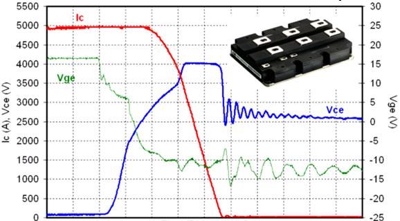
B. IGBT VI. CONCLUSIONS
To improve performance and reduce the size and cost of
By enabling the IGBT to withstand SSCM, the device will power electronic systems, the development trend in high power
exhibit a square SOA capability up to the blocking voltage semiconductors continues towards higher current and power
level. This mode of operation can be seen in the 3.3kV/1200A capabilities. There has always been a pressure on power
IGBT module RBSOA waveforms shown in Figure 9.a and the semiconductor manufacturers, in order to increase the SOA.
associated square SOA I/V curve of Figure 9.b. The presented new benchmark in SOA performances will
The oscillations observed in the current and voltage provide a new outlook for system designers, enabling a far
waveforms (Figure 9.a) after SSCM are a result of the step more optimum performance of high voltage power electronics
response to voltage VSSCM – VDC and the oscillatory circuit applications.
composed of the high stray circuit inductance and the low
device output capacitance during SSCM. ACKNOWLEDGMENT
The author would like to thank the engineers and the
scientists in the R&D Department of ABB Switzerland Ltd.
Semiconductors, who have contributed to the development of
high SOA power semiconductors. Especially the efforts of Dr.
T. Stiasny and Dr. M. Rahimo are highly appreciated.
REFERENCES
[1] K. Yoshikawa et. Al. “A study on wide RBSOA of 4.5kV power pack
IGBT,” Proc. ISPSD 2001, Nuernberg, Germany p. 117
[2] K. Satoh et. Al. “6kV/4kA Gate Commutated Turn-Off Thyristor with
operation DC voltage of 3.6kV,” ISPSD 1998,. Nuernberg, Germany
(a) [3] H. Gruening et. Al. “ A new compact high di/dt gate drive unit for 6 inch
GCTs”, ISPSD 2004
[4] T. Stiasny et. Al. “ Large area IGCTs with improved SOA,” PCIM
Nuernberg 2004
[5] J. Oetjen, et.al. “Current filament in bipolar power devices during
dynamic avalanche breakdown,” Solid State Electronics 44, p. 117,
2000.
(b)
Figure 9. (a) 3.3kV IGBT module demonstrating SSCM (0.6 MW/cm2);
(b) Corresponding SOA
3.3kV/1200A IGBT module during Turn-off (24 IGBTs)
Vcc= 2600V, Ic= 5000A, RG= 1.5ohm, Ls= 280nH, Tj= 125°C
Dissipation: 20 J in total, 5 J during self-clamp. 14 MW peak power
no clamp, no snubbers
IAS Page 5 of 5 Tampa, October 2006You can also read