NVMExplorer: A Framework for Cross-Stack Comparisons of Embedded Non-Volatile Memories - arXiv
←
→
Page content transcription
If your browser does not render page correctly, please read the page content below
NVMExplorer: A Framework for Cross-Stack Comparisons
                                                 of Embedded Non-Volatile Memories
                                                                               ∗
                                                       Lillian Pentecost                     Alexander Hankin*                             Marco Donato
                                                        Harvard University                      Tufts University                           Tufts University
                                                       Cambridge, MA, USA                      Medford, MA, USA                           Medford, MA, USA

                                                        Mark Hempstead                           Gu-Yeon Wei                                David Brooks
                                                          Tufts University                     Harvard University                        Harvard University
                                                         Medford, MA, USA                     Cambridge, MA, USA                        Cambridge, MA, USA
arXiv:2109.01188v1 [cs.ET] 2 Sep 2021

                                        ABSTRACT                                                                                                     Figure 1: The number of
                                                                                                                                                     NVM publications from
                                        Repeated off-chip memory access to DRAM drive up op-                                                         VLSI, ISSCC, and IEDM
                                        erating power for data-intensive applications, and SRAM                                                      2016-2020 (cited in text)
                                        technology scaling and leakage power limits the efficiency                                                   shows strong interest in
                                        of embedded memories. Future on-chip storage will need                                                       RRAM and STT and
                                        higher density and energy efficiency, and the actively ex-                                                   an emergence of newer
                                        panding field of emerging, embeddable non-volatile memory                                                    technologies, such as
                                        (eNVM) technologies is providing many potential candidates                                                   ferroelectric-based ones.
                                        to satisfy this need. Each technology proposal presents dis-
                                        tinct trade-offs in terms of density, read, write, and reliabil-
                                        ity characteristics, and we present a comprehensive frame-             of highly specialized architectures with the benefits of non-
                                        work for navigating and quantifying these design trade-offs            volatile memories by leveraging analog compute capabil-
                                        alongside realistic system constraints and application-level           ities [26, 33, 122, 131]. On the other hand, the need for
                                        impacts. This work evaluates eNVM-based storage for a                  optimized on-chip storage solutions and memory innova-
                                        range of application and system contexts including machine             tion applies both to specialized hardware accelerators and
                                        learning on the edge, graph analytics, and general purpose             for general-purpose CPU systems as well. More broadly,
                                        cache hierarchy, in addition to describing a freely available          prior works have unveiled incredible potential improvements
                                        (http://nvmexplorer.seas.harvard.edu/) set of tools                    in storage density and energy efficiency by employing eN-
                                        for application experts, system designers, and device experts          VMs across various architecture domains [56, 63, 115]. With
                                        to better understand, compare, and quantify the next genera-           many publications showcasing the benefits of eNVM storage
                                        tion of embedded memory solutions.                                     technologies, it is critical for system designers to be able
                                                                                                               to explore their varying capabilities and empower efficient
                                        1.   INTRODUCTION                                                      future on-chip storage. Unfortunately the architecture and
                                           The wide adoption of data-intensive algorithms to tackle            broader research community lacks a holistic tool to identify
                                        today’s computational problems introduces new challenges               and quantify the system and application-level implications of
                                        in designing efficient computing systems to support these              memory cell technologies and to make informed decisions
                                        applications. Hardware specialization has shown potential in           while navigating the vast eNVM design space.
                                        supporting state-of-the-art machine learning and graph analyt-            Figure 1 summarizes device and circuit conference publi-
                                        ics algorithms across several computing platforms; however,            cations relating to eNVMs from 2016 to 2020 [3, 4, 5, 6, 7, 8,
                                        data movement remains a major performance and energy bot-              10, 12, 13, 14, 16, 18, 19, 22, 23, 24, 25, 27, 28, 29, 30, 31, 32, 34,
                                        tleneck. As repeated memory accesses to off-chip DRAM                  35, 36, 39, 41, 42, 43, 44, 45, 46, 47, 48, 49, 50, 51, 52, 53, 54, 57,
                                        impose an overwhelming energy cost, we need to rethink the             58, 59, 60, 61, 62, 64, 65, 66, 67, 68, 69, 70, 71, 72, 74, 76, 77, 78,
                                        way embedded memory systems are built in order to increase             79, 80, 81, 83, 84, 85, 86, 87, 88, 89, 90, 91, 92, 93, 94, 95, 96, 97,
                                        on-chip storage density and energy efficiency beyond what is           98,99,100,101,102,103,104,105,106,107,108,109,111,113,
                                        currently possible with SRAM-based solutions.                          118, 120, 121, 125, 126, 127, 128, 130, 132, 133, 134, 135, 136,
                                           In recent years, CMOS-compatible, embedded nonvolatile              137, 138, 139, 140, 141, 142, 143, 144, 145, 147, 148, 149, 150,
                                        memory (eNVM) research has transitioned from articles and              151, 152, 153, 154, 155, 156, 157, 158, 159, 160, 161, 162]. In
                                        technical reports to manufacturing flows and product lines.            the past five years, consistent interest in RRAM and STT was
                                        These technologies hold incredible promise toward overcom-             accompanied by emerging solutions with different physical
                                        ing the memory wall problem. For example, one approach                 properties such as FeFET-based memories. Each published
                                        inspired by these new technologies combines the advantages             example offers compelling and distinct trade-offs in terms of
                                                                                                               read and write characteristics, storage density, and reliability.
                                        ∗Authors contributed equally to this work.                             In addition, the space of eNVM technologies is constantly

                                                                                                           1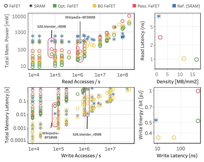
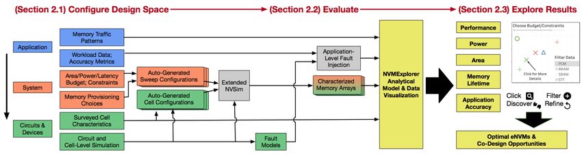
Figure 2: NVMExplorer framework overview; cross-stack design space specifications and application characteristics
are evaluated in an efficient multi-stage process, then displayed in an interactive set of data visualizations to enable
informed, application-aware comparisons of future on-chip storage solutions, as described in more detail in Section 2.
evolving with certain technologies moving out of fashion or             After describing NVMExplorer (Section 2), we present a
into production. Given the fluidity and complexity of this           snapshot of the current eNVM landscape and extract a repre-
design space, application experts and system designers need          sentative range of cell-level behavior (Section 3). Surveying
to be able to evaluate which cell technologies are most likely       recent eNVM publications reveals diverse characteristics,
to provide better efficiency, higher storage density, or im-         highlighting the challenge in identifying solutions that sat-
provements on other key metrics in the context of different          isfy a broad range of application scenarios. Thus, Section
computing demands. Similarly, device designers and memory            4 presents application-driven case studies using NVMEx-
architects need high-level guidance to co-design their innova-       plorer to explore and analyze eNVM storage solutions for
tions toward more practical and maximally beneficial future,         DNN inference acceleration, graph processing, and general-
heterogeneous memory systems.                                        purpose compute. We find that each eNVM is viable in cer-
   This work introduces NVMExplorer, an end-to-end de-               tain contexts, and the most compelling eNVM is dependent
sign space exploration framework that addresses key cross-           on application behavior, system constraints, and device-level
stack design questions and reveals future opportunities across       choices. This finding suggests the existence of many possi-
eNVM technologies under realistic system-level constraints,          ble architecture-device co-design opportunities, which is the
while providing a flexible interface to empower further in-          focus of Section 5. Finally, we differentiate NVMExplorer
vestigations. In this work, we describe NVMExplorer and              from related tools (Section 6).
present case studies made uniquely possible by the capabili-
ties of NVMExplorer. In summary, NVMExplorer makes the
following key contributions to the research community:               2.     NVMExplorer
                                                                        At a high level, NVMExplorer is a comprehensive design
    • An open-source code base including:
                                                                     space exploration (DSE) framework integrating application-
        – A database of eNVM cells described in recent               level characteristics, system constraints, and circuit and de-
          literature (122 surveyed ISSCC, IEDM, and VLSI             vice parameters in a publicly-available, simple-to-use flow.
          publications) (Section 3.1)                                The overall structure of NVMExplorer (Fig. 2) relies on three
        – A “tentpole” methodology to summarize limits               stages, described in more details in the following subsections:
          and trends across technology classes (Section 3.2)
                                                                          1. A comprehensive cross-stack configuration interface to
        – Our end-to-end evaluation flow (Fig. 2)
                                                                             specify the design space of interest. This configuration
        – Extensive source-code documentation                                spans the computing stack from application (blue) and
        – Many example configuration files and tutorial ma-                  system (orange) down to circuits and devices (green).
          terials for cross-stack design studies
        – An interactive web-based data visualization dash-               2. An evaluation engine which automatically generates
          board (Section 2.3)                                                configurations, simulates memory arrays, processes ap-
   • A unified platform to explore the viability of eNVMs in                 plication behavior, computes key metrics such as perf,
     specific application and system settings, which reveals                 power, area, accuracy, and lifetime, and generates mean-
     cross-stack dependencies and optimization opportuni-                    ingful visualizations. Evaluation steps which are exten-
     ties, in addition to reproducing and expanding previous                 sions of existing tools are shaded grey in Fig. 2.
     published studies, (e.g., [115] [56]) (Section 4).
                                                                          3. An interactive, web-based visualization tool to aide
   • A unified platform to perform co-design studies of ap-                  discovering, filtering and refining eNVM design points.
     plication properties, system constraints, and devices in
     order to bridge the gap between architects and device             NVMExplorer is publicly available at
     designers for future eNVM solutions. Our example co-            http://nvmexplorer.seas.harvard.edu/and the source
     design studies reveal both opportunities and potential          code is available at https://github.com/lpentecost/
     disconnects among current research efforts (Section 5).         NVMExplorer.

                                                                 2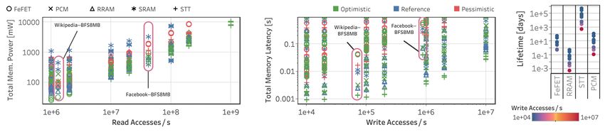
Figure 3: For fixed capacity (4MB) and under various optimization targets, array-level metrics reveal each eNVM has
unique, compelling attributes. Note Pessimistic PCM write latency (> 10µs) is omitted for clarity in the write energy vs.
write latency plot above.
2.1    Cross-Stack Configuration                                        rics. NVMExplorer combines a customized memory array
   To evaluate and compare eNVM solutions in system set-                simulator, an application-level fault injection tool, and an
tings, it is not just cell or even array-level characteristics of       analytical model to extrapolate application-level performance
a particular technology that matter. Rather, viable solutions           metrics.
depend on the area/power budget of a system and how ap-                    To characterize memory arrays, we rely on a customized
plications running on that system interact with the memory.             version of NVSim, a previously validated tool to compute
NVMExplorer provides a rich interface for configuring key               array-level timing, energy, and area [40]. We build on existing
application, system, and circuit and device parameters.                 efforts to extend NVSim to support multi-level cells and
   At the application level, the user inputs information about          ferroelectric-based eNVMs [115, 123]. In addition, we have
memory traffic, which may include the number of read and                modified the tool interface to ease data collection and post-
write operations, their proportion relative to the total number         processing. We introduce the capabilities of NVMExplorer in
of memory accesses, and how accesses are spread out over                comparing eNVM candidates in Section 2.2.1. Results of cell-
execution time. These configuration parameters may be fixed             level and circuit-level simulations can be used to parameterize
values (e.g., characterization results of a specific workload)          fault models and perform application-level fault injection,
or provided as ranges to generate generic memory traffic                as described in Section 2.2.2. The analytical model takes
patterns. Some applications may have additional demands                 application access counts, system settings like datawidth, and
or metrics which are tightly related to memory technology               array-level results like energy/latency per access and leakage
characteristics. For example, machine learning applications             power to compute the total memory power and access latency
or approximate computing methods may trade-off relaxed                  during operation.
accuracy for performance and energy, and NVMExplorer also
provides an interface for designers to study the application            2.2.1    Example Array-Level Comparison
interactions and implications of fault-prone eNVM solutions.
   At the system level, the user has the freedom to evaluate a             Figure 3 presents example array characterization output
wide variety of memory configuration options by either set-             generated by NVMExplorer after evaluating various eNVM
ting performance, power, and area constraints and optimiza-             configurations implemented in a 22nm node. The design
tion goals or by choosing memory array specifications such              points are color-coded to highlight optimistic (green), pes-
as capacity, multi-level programming, bank configuration,               simistic (red), or reference (blue) designs across surveyed
and more. The circuits and devices level of the design space            publications per cell technology. The figure also reports the
configuration comprises per-technology memory cell char-                characteristics of 16nm SRAM as a comparison point. For
acteristics, in addition to sensing and programming circuitry           each technology, we show array characterization under differ-
choices. NVMExplorer also provides a database of eNVM                   ent optimization goals, which result in a variety of internal
cell configurations derived from ISSCC, IEDM, and VLSI                  array architectures. For example, we observe a wide range
publications, as described in Section 3, but it is also possible        for the read-energy-per-bit of an iso-capacity SRAM array.
(and encouraged!) for users to extend the current NVMEx-                This result reflects the effect of different array optimization
plorer database with new simulation-based (i.e. SPICE or                targets (read energy-delay product, write characteristics, area)
TCAD models), measured, or projected circuit and device                 on the internal bank configuration and periphery overhead,
properties. Once the full-stack specifications are set, NVM-            resulting in disparate array layouts.
Explorer automatically generates configuration files, which                This preliminary study already provides a few key take-
are used as input to the evaluation engine.                             aways. Each eNVM is able to attain read access characteris-
                                                                        tics competitive with SRAM, with the exception of an array
                                                                        characterized with pessimistic underlying PCM cell character-
2.2    Evaluation Engine                                                istics. However, write access characteristics vary dramatically
   Given the auto-generated cell and system-level sweep con-            across published eNVM examples, in addition to the range
figurations, the evaluation engine produces memory array                of reported endurance per technology. The tension between
architecture characterizations and computes application- and            these properties and potential storage density (even in the
system-level power, performance, area, and reliability met-             absence of multi-level cell programming) indicates that array-

                                                                    3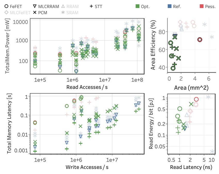
SRAM        PCM         STT         SOT       RRAM            CTT       FeRAM         FeFET
         Cell Area [F 2 ]       146       25-40       14-75       [20]        4-53           1-12                    4-103
         Tech. Node [nm]       7-16      28-120       22-90      [1000]      16-130         14-16        40           45
         MLC                    no         yes         yes         yes         yes           yes         yes          yes
         Read Latency [ns]    0.5-1.5    [1-100]     1.3-19     1.4-11      3.3-2e3                      14
         Write Latency [ns]   0.5-1.5    10-3e4       2-200     0.35-17       5-1e5    6e7-2.6e9       14-1e3     0.93-1.3e3
         Read Energy [pJ]     1.1-2.4               0.21-1.2                   1e-3                     0.001
         Write Energy [pJ]    1.1-33                 0.6-4.5    [0.015-8]      0.68                               0.0003-0.01
         Endurance [Cycles]    N/A      105 –1011   105 –1015               103 –108        104       104 –1011     107 -1011
         Retention [s]         N/A      108 –1010      108        108       103 –108        108       105 –108

Table 1: High-level listing of memory cell technologies and ranges for key characteristics; recent publications are
complemented by simulation and industry references to form technology cell definitions discussed in Section 3.1.
level comparison in isolation may guide a system designer                              choices, and/or eNVM cell configurations) alongside array-
towards sub-optimal solutions. For example, a FeFET-based                              level metrics for a holistic design exploration experience. A
memory may seem a fitting choice for high-density, read-                               user can filter results in terms of important constraints (e.g.,
performant storage, but we find that both performance and                              latency or accuracy targets, power or memory area budget)
energy efficiency of those memories are highly shaped by                               and identify design points of interest. While several features
application traffic patterns and underlying cell assumptions.                          of these visualizations, built using Tableau [9], are evident in
Thus, the cross-stack nature of data exploration supported by                          the figures in this work, including dynamic filtering across
NVMExplorer is essential in guiding system-level choices                               plots, click-and-drag to narrow the design space, and pop-up
and further investigation.                                                             details about results, we encourage the reader to use their
                                                                                       imagination in how they might explore and filter the data
2.2.2    Fault Modeling and Reliability Studies                                        shown in alternative ways according to their interests, ques-
   In addition to characterizing memory performance, power,                            tions, or confusions.
area, and lifetime, NVMExplorer extends previously vali-
dated efforts in application-level fault injection to provide                          3.      TECHNOLOGY LANDSCAPE
an interface for fault modeling and reliability studies [119].                            NVMExplorer provides a broad survey of published eNVM
Users can provide an expected error rate or more detailed,                             examples (Section 3.1), which can be parameterized so that
technology-specific fault models and storage formats to per-                           systems experts can make meaningful, high-level compar-
form fault injection trials on application data stored in differ-                      isons across technologies despite different underlying trade-
ent eNVMs. To quantify the impact on application-specific                              offs and maturity (Section 3.2). We validate this approach
metrics of accuracy, the fault injection tool is tightly inte-                         per-technology against fabricated memory arrays (Section
grated with application libraries for data-intensive workloads,                        3.3).
including PyTorch for DNNs and snap for graph process-
ing [82, 114], as well as numpy for generic application data.                          3.1          Cell Definitions
As a demonstration, we perform SPICE simulation and ex-                                   We compile device- and array-level data across eNVM
tract fault charactieristics associated with single-level vs.                          technologies including PCM, STT, SOT, RRAM, CTT, FeRAM,
multi-level cell (SLC vs. MLC) programming and sensing                                 and FeFET-based memories. The results of this survey in-
circuitry characteristics. In this work, we consider a sub-                            clude read-write characteristics, endurance, and density, as
set of eNVMs, namely, RRAM, CTT, and FeFET, whose                                      summarized in Table 1 alongside SRAM properties. We
fault characteristics could be derived from existing model-                            source the majority of the cell-level parameters from ISSCC,
ing efforts [115, 123]. We use our extended fault injection                            IEDM, and VLSI publications and focus primarily on works
framework to simulate the impact of storing workload data                              from 2017-2020 to reflect the most recent range of achievable
in SLCs vs. MLCs in Section 5.3. Armed with these addi-                                behavior per technology. Previous efforts have detailed the
tional capabilities, NVMExplorer can replicate the results of                          physical properties and limitations per technology [20], while
previous considerations of eNVM storage reliability [115], in                          NVMExplorer focuses on compiling sufficient cell-level de-
addition to providing a broader platform for studying the in-                          tails and leaning on existing technology models to provide
teractions between programming choices, cell characteristics,                          a broad and practical database of cell definitions. While
and application accuracy.                                                              we hope these extracted cell definitions are helpful to the
                                                                                       community in calibrating the current state-of-the-art, NVM-
2.3     Exploring Results & Conducting Studies                                         Explorer is extensible to alternative devices as the design
   The figures in this work are snapshots from NVMEx-                                  space continues to evolve, as demonstrated in Section 5.
plorer’s interactive web-based data visualization tool, which                             The technology classes in Table 1 are at different levels of
will be freely available at the time of publication of this work                       maturity. For example, SOT is a relatively recent technology,
at http://nvmexplorer.seas.harvard.edu/. In each                                       and while it boasts very impressive write speed and lower
study, we filter and constrain evaluated results according to                          write current compared to STT, it is not yet published at
system optimization priorities and application use cases, as                           advanced process nodes. We also see that endurance varies
described in the text. The basic NVMExplorer data visualiza-                           by multiple orders of magnitude across different technologies.
tion dashboard presents power, performance, area, and mem-                             Thus, adoption will depend on the write intensity of target
ory lifetime results across all user-configured sweep results                          applications and system dynamics, so incorporating memory
(e.g., many application traffic patterns, array provisioning                           lifetime estimation becomes a critical design consideration.

                                                                                 4
Grey cells in Table 1 indicate parameters unavailable in
recent publications. This could be for reasons of propriety
from industry fabrication or experimental constraints. How-
ever, for architects, it is important to have some concept of
the possible range of values associated with these parameters.
In those cases where SPICE models for a technology are
available, we use simulations to fill in missing parameters.
Alternatively, we consider older publications and consult with
device experts to reason about cell and array parameters.
                                                                      Figure 4: “Tentpole” STT vs. published array data
3.2     Tentpoles of the Design Space                                 shows coverage of the space across critical metrics.
   Comparing eNVMs at varying stages of development and
with varying underlying physical properties is a challenging          models and error rates for reliability studies are extracted
task. The case studies in this work aim to provide high-level         after optimistic vs. pessimistic cell-level properties are fixed,
guidance and relative judgments about which eNVM cell                 as discussed in one of the presented case studies (Section
technologies are worthy of further investigation under spe-           5.3).
cific system and application constraints. Thus, rather than              This approach helpful for many reasons: for one, these
focus in on specific, physically accurate cell configurations,        extremes help us answer exploratory questions about what
we aim to model the bounds of what is conceivable per eNVM            we will likely see in the near future; secondly, comparing
technology across the full range of published recent academic         the best-case of one technology to the worst-case of another
work. We liken identifying and evaluating these bounds per-           can help gauge less mature technologies against more mature
technology to forming the poles of a tent that encompasses            reference points; thirdly, if such optimistic configurations are
the full extent of eNVM properties, so we call the extrema            untenable or even pessimistic configurations are attractive in
in terms of cell-level characteristics (i.e., smallest, lowest        a specific system setting, we can build confidence for further
read energy, best retention vs. largest cell size, lowest en-         exploration and more detailed modeling efforts without im-
durance) the device-level “tentpoles”. In an actively evolving        plementing and attempting to meaningfully compare many
technology space, this approach allows us to make meaning-            many cell definitions with insufficient data. A limitation of
ful classifications about which technologies are potentially          this methodology is that inherent trade-offs between certain
adoptable solutions. These modeling choices are classified            parameters for a technology may not be linked (e.g., area, la-
into two fixed cell configurations for applicable technologies,       tency, and retention for STT); however, this amalgam of cell
as summarized in Section 3.2.1 and the figure alongside Table         properties represent the full spectrum of achievable character-
1. We validate that the “tentpoles” of the cell-level design          istics per technology, rather than specific fabricated results.
space result in array-level characterization that provides cov-       As a point of additional comparison, the results shown in
erage of published memory array properties, as discussed in           the following studies include a reference cell configuration
Section 3.3.                                                          for RRAM as a relatively mature eNVM, with parameters
                                                                      derived from a specific industry result [31]. The resulting
3.2.1    Optimistic and Pessimistic Cell Configurations               optimistic, pessimistic, and reference cell size and write pulse
   For the technology classes most represented in our sur-            are shown to the right of Table 1.
vey (Fig. 1), we compute which published example has the
best-case and worst-case storage density in terms of Mb/F2 ,          3.3    Validation
and this data serves as the foundation of the bounds of the              Our array-level area, energy, and latency characterizations
cell-level design space; those points which are most and least        rely on the previously-validated procedures of NVSim to
dense across recent published examples. Any critical cell-            extrapolate cell-level configurations and array design con-
level parameters not reported with those cell definitions are         straints to optimized memory layouts and properties [40].
assigned values (e.g., read characteristics and programming           However, in employing our “tentpole” approach, it is critical
settings) using the best (lowest power, highest efficiency)           that we verify that array-level results using our optimistic
or worst (highest power, lowest efficiency) value per metric          and pessimistic underlying cell characteristics fully cover and
across all other recent publications with sufficient supporting       match expectations of existing fabricated eNVM solutions.
data. These best-case and worst-case technologies per class              Whenever possible, we select publications with array-level
form the tentpoles of the underlying cell design space, and           characterizations for a given technology, and compare those
we label these fixed cell definitions as “optimistic” or “pes-        results to iso-capacity memory arrays modeled through our
simistic” accordingly. For the purposes of the case studies           “tentpole” approach. Figure 4 shows an example of such an
presented in Sections 4 and 5, all array- and application-            exercise. We compare a 1MB STT-RAM array published
level results are produced using these fixed underlying opti-         at ISSCC in 2018 to optimistic and pessimistic STT design
mistic and pessimistic cell properties, though we note that a         points produced by NVMExplorer. Here, we note that our
user of NVMExplorer can draw either on these constructed,             tentpole results effectively represent the range of actual ar-
bounding example cells or on the full database of surveyed            ray properties by producing metrics that are both higher and
configurations, or on fully customized definitions with re-           lower, but similar in magnitude, to the reference STT-RAM
spect to cell size, access properties, and operating conditions       array. The studies presented in this work consider only vali-
(e.g.,read/write voltage, temperature). Corresponding fault           dated configurations for which we were able to either com-

                                                                  5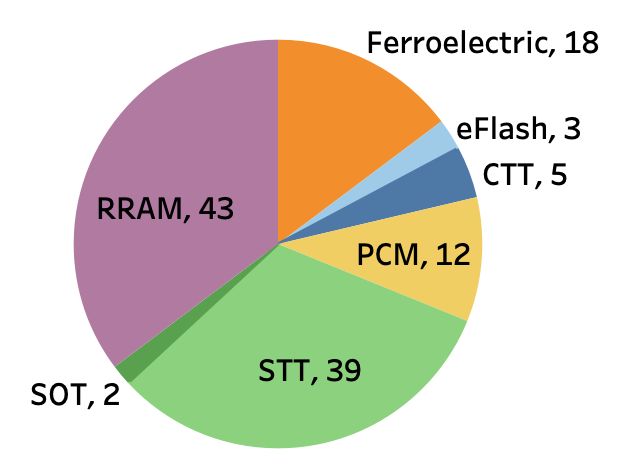
Figure 6: The most energy-efficient eNVM varies under
                                                                        different DNN inference use cases, such as continuous
                                                                        (left, operating power) vs. intermittent (right, report-
Figure 5: Read characteristics and storage density for                  ing energy per input image frame); these results exclude
2MB arrays, provisioned for replacement of on-chip                      eNVM solutions that are unable to meet application la-
SRAM in NVDLA.                                                          tency and accuracy targets.

plete this validation exercise or run SPICE-level simulations.
It is worth noting that NVMExplorer is set up to evaluate all
technologies in Table 1 following more rigorous validation or
future publications. System validation and application charac-
teristics are derived from existing, state-of-the-art references,
as addressed in each study in Section 4.

4.    APPLICATION-DRIVEN CASE STUDIES                                   Figure 7: The eNVM storage solution (iso-capacity ar-
   We now present three case studies that highlight different           rays provisioned per task, optimized for ReadEDP) that
ways NVMExplorer can search design spaces in order to                   minimizes total memory energy consumption varies ac-
identify benefits and limitations of the diverse range of eNVM          cording to system wake-up frequency and DNN inference
storage solutions. Each scenario presents unique optimization           task; All solutions shown maintain application accuracy
goals and system priorities and, in each case, we compare how           and a < 1s latency per inference.
each eNVM’s power, performance, and area fairs relative to
similarly-provisioned SRAM or DRAM in a baseline system.                   First, we observe the read and storage density characteris-
                                                                        tics for 2MB arrays using the cell-level tentpoles of several
4.1     DNN Inference Accelerator                                       promising eNVM technology classes, FeFET, STT, PCM, and
   Prior studies have demonstrated the potential benefits of            RRAM, as shown in Figure 5 compared with SRAM. Notice
eNVM storage for Deep Neural Network (DNN) inference                    that read energy effectively divides arrays into two tiers. STT,
accelerators [37, 115, 146], albeit with limited scope in terms         PCM, and RRAM offer lower read energies across a wide
of eNVM technologies and cross-stack parameters consid-                 range of read latency that still outperform SRAM. In contrast,
ered. NVMExplorer empowers researchers to approach a                    FeFET-based eNVMs suffer from higher read energies, but
broader set of questions that compare eNVMs in different                notice that an optimistic FeFET offers the highest storage
storage scenarios (e.g., limited to weights vs. storage of DNN          density with low latency. At similar low latency, optimistic
parameters and intermediate results) and system constraints             STT offers 6× higher density over SRAM. PCM and RRAM
(e.g., strict area budget, or power budget). In this work, we           outperform SRAM in terms of both read latency and stor-
consider two distinct use cases for a DNN inference accelera-           age density. While such comparative insights can readily be
tor: continuous operation, as in image processing per frame             extracted from this pair of plots, there are other important
of a streamed video input, and intermittent operation, where            dimensions to also consider, and NVMExplorer facilitates
the system is woken up per inference task and can leverage              more comprehensive analyses that consider the impact of
the non-volatility of eNVM by retaining DNN parameters                  application priorities and system-level use cases on eNVM
on-chip in power-off state between inferences.                          design decisions.
                                                                           Considering more dimensions of the design space, Fig-
4.1.1    Continuous Operation                                           ure 6 (left) summarizes total operating power (both dynamic
   We consider the commonly-used and well-studied NVDLA                 access and leakage power) for the 2MB memory arrays char-
[129] as a base computing platform and compare its 2MB                  acterized in Figure 5 and accessed according to continuous
SRAM with iso-capacity eNVMs. We use the NVDLA per-                     traffic patterns of different ResNet model deployment scenar-
formance model [110] to extract realistic memory access                 ios, i.e., single- vs. multi-task and weights-only vs. storing
patterns and bandwidth requirements of the on-chip buffer.              both weights and activations. These results exclude eNVM
More specifically, we evaluate the power and performance of             candidates that cannot support 60 FPS operation nor main-
accesses to on-chip memory storing ResNet26 weights for                 tain DNN accuracy targets. Recall NVMExplorer includes
single-task image classification using the ImageNet dataset             fault injection wherein high eNVM fault rates can degrade
vs. multi-task image processing, comprising object detection,           model accuracy to unacceptable levels. While not explicitly
tracking, and classification, at a consistent frame rate of 60          shown here, NVMExplorer considers numerous additional
frames-per-second, as is typical for HD video. We addition-             interactions for users to probe, explore, and build intuition.
ally consider the impact of storing activations in eNVM, but            For example, while total memory power increases as the
this ostensibly ignores endurance limitations.                          number of accesses per frame increases to compute multiple

                                                                    6
tasks, the ratio of read-to-write traffic stays roughly the same. transformer-based DNN [75].
Hence, the relative power of eNVM arrays also remains simi- To further study this result, we dig into the implications of
lar. In particular, PCM, RRAM, and STT all offer over 4× intermittent operation and compare the total energy versus the
reduction in total memory power over SRAM. One important number of inferences per day, showing a continuum of wake-
reason for this is that SRAM leakage power will dominate up frequency that may arise (e.g., deployed solar-powered
compared to eNVM solutions, even under high traffic. Of agricultural sensors or satellites, or a voice-enabled assistant
the energy-efficient solutions, STT offers best performance executing NLP tasks on wake-up). The left plot of Figure 7
(lowest application latency per frame). In contrast, optimistic shows total memory energy as a function of inferences per
FeFET offers higher storage density while maintaining 60FPS day for image classification. Here, total memory energy
and a 1.5-3× power advantage over SRAM. is presented as a proxy for device battery life. From the
figure, we observe that when the number of inferences per day
4.1.2 Intermittent Operation is sufficiently low (less than 1e5), optimistic FeFET yields
Let us now consider eNVM storage for two additional use the lowest energy. At higher wake-up frequency, optimistic
cases that alter system-level optimization goals and corre- STTs take over because of the relatively lower energy-per-
sponding eNVM selection, further highlighting the flexibility access. Figure 7 (right) investigates the impact on an NLP
and ease of exploration the NVMExplorer framework offers. workload. While results are similar, optimistic STT emerges
A major advantage of storing DNN weights in eNVMs is that as the best technology at lower inference rates (as compared
non-volatility supports intermittent operation that powers off to image classification), because ALBERT requires more
the accelerator between inferences. Using SRAMs would computational power per inference than ResNet26.
either consume leakage power to keep the weights memory Table 2 summarizes the preferred eNVM technology across
powered on or consume power to restore the weights from off- different use cases and tasks, with “Opt. eNVM” indicating
chip memory, e.g., by incurring a latency and energy penalty the preferred choice under optimistic underlying cell charac-
by fetching from DRAM. In this use case, we provision mono- teristics and “Alt. eNVM” indicating the preferred technology
lithic eNVM storage to hold all DNN weights (e.g., 8MB for assuming pessimistic assumptions and reference points, and
image tasks and up to 32MB for Natural Language Process- table entries for intermittent operation are selected at a fixed
ing (NLP) tasks). For image processing, all weight memory wake-up rate.
accesses are to eNVM, eliminating the otherwise-required Across a range of device wake-up frequencies and per-
wake-up latency and power associated with loading param- wake-up compute patterns, we observe that several eNVMs
eters into on-chip SRAM, in addition to reducing distance become compelling, and the preferred NVM choice for fur-
between compute system and higher-capacity memory. ther investigation varies depending on both of these factors.
Figure 6 (right) compares the resulting memory-energy-
per-inference across eNVMs for both single-task image clas- 4.2 Enabling Efficient Graph Processing
sification and multi-task image processing, as determined by Our second case study explores the potential benefits of
the total number of accesses to retrieve all DNN weights over using eNVMs for graph processing, which imposes an en-
the course of processing one input frame. The lowest-energy tirely different set of constraints in terms of memory read
technology choice differs between the single vs. multi-task and write characteristics. Graph processing comprises many
inference and, perhaps more interesting, both are eNVM can- read-dominated tasks with less predictable data reuse than
didates with lower storage density (RRAM and pessimistic DNNs (e.g., search kernels), but still involves write traffic
FeFET), as opposed to the highest density options (STT and and, overall, is incredibly data-intensive in terms of mem-
optimistic FeFET), which hints at a cross-stack prioritization ory bandwidth and capacity. As an initial exploration of
of read performance as opposed to cell size reduction, as compatibility and viability between graph processing work-
probed further in Sec. 5.2. We repeat this study for single loads and eNVM storage solutions, we consider the total
task vs. multi-task natural language processing using the AL- power and resulting memory lifetime per technology under
BERT network, a relatively small-footprint, high-accuracy, generic traffic patterns covering the range of read and write
bandwidths for critical graph tasks, as described in previous
workload characterization efforts [11]. As a proof of concept
Use Case Inference Task Data Storage Priority Opt. eNVM Alt. eNVM
Weights Only
Low Power PCM PCM in a specific system, we additionally evaluate eNVM storage
Single-Task
Image Classification
High Density
Low Power
FeFET
PCM
CTT
RRAM
solutions under access patterns for benchmarks executed on
Weights + Acts
Continuous
(60IPS)
High Density
Low Power
STT
PCM
RRAM
RRAM
a domain-specific accelerator [55].
Weights Only
Multi-Task High Density FeFET CTT
Image Processing Low Power STT RRAM
Weights + Acts
Single-Task
High Density
Low Energy/Inf
STT
RRAM
RRAM
RRAM
4.2.1 Analysis for generic traffic patterns
Weights Only
Image Classification High Density FeFET CTT
Multi-Task Low Energy/Inf FeFET FeFET We consider different memories experiencing a range of
Weights Only
Intermittent
Image Processing High Density
Low Energy/Inf
FeFET
RRAM
CTT
RRAM
generic traffic patterns representing graph processing kernels
Embeddings Only
(1IPS) Sentence Classification
(ALBERT)
High Density
Low Energy/Inf
FeFET
STT
CTT
RRAM
(i.e., read access rates from 1-10GB/s and write access rates
All Weights
Multi-Task NLP
High Density
Low Energy/Inf
FeFET
STT
CTT
RRAM
from 1-100MB/s) [11]. NVMExplorer provides a wide array
All Weights
(ALBERT) High Density FeFET CTT of critical metrics to compare and user-configurable visualiza-
tions to extract important trends and limitations. For example,
Table 2: Summary of preferred eNVM under varying in Figure 8, we choose to display total memory power against
DNN use case, task, storage strategy, and optimization read traffic, as number of read accesses becomes a dominant
priority. factor in total power for read-dominated workloads, and total
7Figure 8: Memory power, latency, and projected lifetime for generic traffic patterns encompassing graph processing
demands, including specific graph kernels as labeled. The lowest power solution depends on the expected read traffic.
FeFET solutions fail to match SRAM performance. STT provides superior performance and memory lifetime.
memory latency against write traffic, as overall performance technology node as reported from Cacti [55,112]. We analyze
for several eNVMs is strongly determined by write traffic. the benefits of replacing the 8MB eDRAM scratchpad with
As shown by Figure 8, left, total memory power gener- an iso-capacity eNVM array provisioned to meet the cited
ally increases with read access rate and the lowest power latency target (1.5ns).
solution depends on the application traffic load. For appli- If we exclude RRAM due to low lifetime projections,
cations that exhibit fewer than 107 read accesses per second, FeFET, PCM, and STT all offer significantly lower mem-
optimistic FeFET is a clear winner, while pessimistic FeFET ory power (about 2-10× lower than SRAM) and even pes-
and RRAM are next best candidates. On the other hand, for simistic STT offers consistent performance. These observa-
higher rates of read traffic (e.g., > 108 ), optimistic STT is tions, based on a realistic graph processing use case extracted
best. For mid-range read access rates, PCM and RRAM are from prior work, are consistent with the results generated us-
also viable solutions sometimes offering the lowest power ing generic traffic patterns. Again, optimal technology choice
solution. However, this relationship alone does not dictate depends on system-level optimization goals, and NVMEx-
memory technology choice. A slightly different and more plorer provides critical insights in the presence or absence of
consistent story emerges when we analyze the impact of dif- a specific system solution and simulation results.
ferent eNVMs on overall memory latency (both read and If the high-level goal is to maximize storage density, Fe-
write) versus write access rates, shown by the middle plot FET is highly attractive, but severely limited by poor write la-
of Figure 8. While there is a clear preference for optimistic tency (unable to meet application latency expectations under
STT, RRAM and optimistic PCM are also worth consider- the higher range of traffic patterns). Rather than prematurely
ing. In contrast, most pessimistic eNVM technologies and all eliminating FeFET, designers can leverage NVMExplorer to
FeFET-based solutions are significantly inferior, even failing study the impact of relaxing or adapting application targets or
to match SRAM performance for many traffic patterns. to explore co-design solutions that target improvements to the
When we additionally consider projected memory lifetime, underlying technology (Sec. 5.1) or architecture (Sec. 5.4).
STT emerges the clear winner overall. Note that the right
chart of Figure 8 plots the memory lifetime assuming contin- 4.3 Non-Volatile LLC Solutions
uous operation at a particular write access rate. Hence, the Improved density and energy efficiency could revolutionize
highest write traffic always yields the lowest lifetime. While general-purpose on-chip storage, and recent efforts have en-
RRAM seemed promising based on performance and power, deavored to replace high-performance memories, like caches,
it has the worst endurance and lowest lifetimes. with eNVM-based alternatives [56, 63, 73]. However, caches
must handle a large volume of writes depending on the ap-
4.2.2 Analysis for domain-specific systems plication, so the achievable write latency and endurance per
In addition to relying on generic traffic patterns to represent eNVM comes to the forefront of design considerations.
the full range of expected traffic loads of graph processing, In this study, we consider the last-level cache (LLC) of a
NVMExplorer can also be leveraged to answer a more spe- high-performance desktop processor, similar to Intel’s 14nm,
cific design question: For performance targets and traffic 8-core Skylake. The memory hierarchy includes a private
patterns to a specific storage resource in a graph processing 32 KiB L1I$; a private 32 KiB L1D$; a private 512 KiB
accelerator system, which eNVMs offer compelling charac- L2$ (non-inclusive, write-back); and a shared ring 16MiB
teristics that warrant further investigation? To this end, Fig- L3$ with 64 B line, 16 ways (inclusive and write-back). The
ure 8 also includes points, identified in pink, corresponding to system includes DRAM with 2 channels, 8 B/cycle/channel,
memory traffic to run breadth-first search on two different so- 42cycles + 51 ns latency. Representative application behav-
cial network graphs (Wikipedia and Facebook) [82]. Traffic ior comes from SPECrate CPU2017 (integer and floating
patterns are extracted from throughput and accesses reported point), and we warm-up the cache for 500M instructions
for the compute stream of a domain-specific graph processing and simulate for 1-billion instructions in detail using the
accelerator utilizing an 8MB eDRAM scratchpad [55]. In Sniper simulator [15, 17]. This provides application mod-
the baseline system, about 90% of the energy is spent on the eling data for a 16MB LLC (e.g., reads, writes, execution
eDRAM scratchpad (not including DRAM controller energy), time per benchmark) that are inputs to NVMExplorer (see
with an operating power of at least 3.1W at the 32nm process Section 2.1).
8Figure 9: Memory operating power, latency, and projected lifetime under continuous operation across SPEC bench-
mark traffic to a 16MB LLC shows preferred eNVM depends on traffic demands and optimization goal. All solutions
shown meet per-benchmark read/write demands. For high-traffic benchmarks, STT provides lowest power, lowest
latency, and longest projected lifetime.
5. CO-DESIGN OPPORTUNITIES
Exploration of the design space in Section 4 shows that no
single eNVM technology is best. Rather, technology choice
depends on the application and system-level targets. This
also means there are ample co-design opportunities across the
computing stack – from devices to architecture. By contex-
tualizing and evaluating high-level implications of cell-level
innovations as they emerge, one can identify what system-
level opportunities are unlocked by that change.
Figure 10: Array access characteristics in isolation for 5.1 Alternative FeFET fabrication choices
consideration of replacing (iso-capacity) a 16MB LLC. unlock performant solutions for
graph processing
First we focus on the array characteristics of the different Previous FeFET-based device characterization and model-
memory technologies in isolation, as shown in Figure 10. ing efforts have exhibited write pulses on the order of 100ns-
From the left plot, we note a competetive range of read en- 1µs. However, alternative FeFET fabrication strategies in
ergy and read latency does not reveal a clear winner. For early development stages, such as back-gated FeFETs [124],
example, if read energy per access is highest priority, FeFET, offer compelling potential advancements in write latency
RRAM or even SRAM offer array configurations that trade (10ns programming pulse) and projected endurance (1012 ).
access latency for energy efficient, while STT and optimistic Section 4.2 noted that the primary limition of FeFETs in
FeFET offer pareto-optimal read characteristics. For writes the context of graph processing was an inability to meet the
(Figure 10, right), a PCM-based last level cache appears to application latency targets under higher write traffic. Thus,
minimize energy per access. On the other hand, only STT and using the underlying cell properties of back-gated FeFETs
RRAM are able to beat SRAM write latency. Again, we find reported in [124], we can rapidly re-examine the viability of
array characteristics in isolation do not offer sufficient guid- FeFET-based memory and probe whether this change could
ance to choose the best eNVM for LLC, and NVMExplorer make a difference in the viability of FeFET-based memory
allows us to go further. for graph processing.
Figure 9 shows the resulting power, performance, and Figure 11 shows the total memory power and total memory
lifetime when using different eNVMs as LLC and assum- latency of an 8MB memory array of back-gated FeFETs (in
ing memory traffic from SPEC2017 benchmarks. The left- yellow) compared to using previous FeFET standards (red,
most figure shows total memory power versus read access green) and SRAM (blue). We examine these metrics under a
rate, where each column of points corresponds to a particu- range of read and write traffic patterns which are inclusive of
lar benchmark traffic pattern. We again see that the lowest the graph benchmarks described in Section 4.2 and the SPEC
power eNVM solution depends on the traffic pattern. In broad benchmarks used in Section 4.3, but here showing access pat-
terms, RRAM and FeFET fair better for lower read access terns for an 8MB capacity LLC. The underlying array-level
rates while PCM is better for higher rates until STT emerges characterization is shown in Figure 11, right. From the ar-
best for the highest rates. In terms of memory access la- ray characterization, we observe that the back-gated FeFETs
tency with respect to write access rates, STT is usually the show a slight increase in read energy per access and slight
best choice, though arrays unable to meet application band- decrease in storage density compared to prior state-of-the-art
width are excluded. Lastly, the rightmost figure compares cells. However, we observe that they enable comparable ap-
lifetimes across the eNVM technologies for a range of write plication latency to SRAM across a wide range of write traffic
access rates. Again, STT offers the best longevity on average. where previous FeFET versions fall short. Furthermore, back-
However, PCM and FeFET may warrant consideration for gated FeFETs results in the lowest operating power over most
read-dominated workloads. RRAM, on the other hand, does of the range of read accesses per second, including for the
not appear viable as an LLC. example graph processing benchmark, Wikipedia–BFS8MB.
95.2 Trade area efficiency for performance
One theme we can highlight across the architecture-driven
case studies from Section 4 is that the subset of character-
ized results that exhibit lower area efficiency (i.e., internal
array architectures that do less amortization of periphery and
sensing overhead) also tend to result in lower total memory
latency across many traffic scenarios. This is perhaps counter-
intuitive given the effort spent in the devices community to
manufacture very small cell sizes. We also note that in Figure
12, where such design points are highlighted across the plots,
that slight advantages in terms of energy-per-access (e.g.,
Opt. STT and PCM compared to FeFET) tend to correlate
to large total power advantages in high-traffic scenarios. As
such, pointing out to device designers the greater relative
impact of reduced energy per access rather than decreased
cell size could usher in a more productive, product-ready
set of eNVM technologies. Additionally, we observe that
Figure 11: Back-gated (BG) FeFETs provide the high reducing energy per write access for STT and RRAM would
density and low operating power for example graph drastically improve their relative power advantage for data-
processing benchmarks with SRAM-comparable perfor- intensive applications, even at a cost of relatively lower area
mance and begin to close the performance gap between efficiency or storage density.
non-BG FeFET and other memory technologies across
SPEC2017 benchmarks.
Based on these observations, we can conclude that back-
gated FeFET memory may close the performance gap be-
tween non-BG FeFET and other memory technologies (in-
cluding SRAM) and unlock additional application domains.
NVMExplorer’s ability both to quickly and efficiently gauge
the impact of cell-level innovations and to match emerging
device designs to compelling use cases can enable produc-
tive future co-design collaborations. This feedback loop is
mutually beneficial in providing direct motivation for further Figure 13: When we consider multi-level cell (MLC) stor-
device development and encouraging system designers to in- age and filter out 8-16MB capacity arrays that don’t pro-
tegrate more energy-efficient, highly dense on-chip memory. vide acceptable ResNet18 inference accuracy after fault
injection trials, we note MLC RRAM offers denser, more
performant memory than SLC RRAM while meeting ap-
plication accuracy, while MLC FeFET is only sufficiently
reliable for larger cell sizes (red points).
5.3 Advantages of multi-level programming
vary among eNVMs
While programming multiple bits per memory cell is an
important strategy for increasing storage density across many
eNVMs, previous work has revealed that MLC eNVMs often
exhibit significantly higher fault rates that must be carefully
considered in conjunction with application resilience [115].
NVMExplorer enables efficient and broad probing of reliabil-
ity vs. storage density by providing an application-agnostic
fault injection tool and templates for technology-specific fault
modes, as discussed in Section 2.2.2. To demonstrate, we
evaluate the impact of density on application accuracy for
ResNet18 weights (image classification) under storage in
Figure 12: Results for 8MB arrays are filtered according SLC vs. 2-bit MLC across multiple technologies which pro-
to a maximum area efficiency bound in the top right plot. vide MLC capabilities and for which there exists sufficient
Arrays with lower area efficiency are highlighted across cell and circuit level modeling to produce detailed fault mod-
all views and tend to result in low memory latency across els. The density vs. reliability trade-off is distinct for each
many traffic scenarios. technology. For example, Figure 13 displays 8MB and 16MB
characterized arrays, including 2-bit MLC RRAM and 2-bit
10est power solution for this particularly high-traffic workload.
STT and RRAM are still the optimal technology choices
for SPEC2017 in terms of performance, but write-buffering
could empower FeFETs as a lower-power alternative if la-
tency could be masked or write traffic to the eNVM could be
reduced by at least 25%.
6. RELATED WORK
Figure 14: Masking write latency or reducing write traf- Previous work in evaluating eNVM technologies can be
fic via introduction of a write caching scheme could en- characterized by either focusing on device- and array-level
able a broader set of eNVM technologies. evaluations, or providing in-depth cross-stack evaluations
based on particular combinations of eNVM devices and ap-
MLC FeFET, filtered such that only those arrays meeting plication targets. In Table 3, we codify the key differences
application latency requirements and maintaining image clas- between NVMExplorer and related works. Survey works
sification accuracy are included. Note that these results repli- such as the Stanford Memory Trends [2] maintain a list of
cate previous efforts that indicate that image classification key eNVM parameters, like storage capacity and write energy,
inference is robust to 2-bit MLC RRAM storage (we also while previously validated array-level characterization tools,
verified this for CTT-based memories with fault modeling de- such as NVSim [40], characterize timing, energy, and area of
tails provided in [38, 115]), while we show that MLC FeFET eNVM-based memory structures. DESTINY [117] modifies
devices only exhibit acceptable accuracy for larger cell sizes. NVSim to evaluate 3D integration and could be similarly
This is because smaller FeFETs are more difficult to program extended and used as a back-end characterization tool for
reliably due to device-to-device variation [123]. Portions of NVMExplorer.
NVMExplorer were leveraged to quantify cell- and circuit- To evaluate eNVMs in a system setting, prior work typ-
level trade-offs specific to MLC FeFETs in greater depth to ically integrates NVSim with a system simulator. Deep-
determine optimal cell provisioning and writing schemes for NVM++ [63] enables design-space exploration of MRAM-
target applications [123]. based technologies in the context of GPU cache for DNNs
using GPGPUSim. NVMain [116] enables evaluation of
5.4 Write buffering changes the performance eNVM-based main memory using gem5. NeuroSim+ [21]
landscape focuses on evaluation of processing-in-memory for DNN in-
In conjunction with technology innovations to reduce write ference and training using eNVMs. Existing works such as
latency, adoption of a wider set of eNVMs in general-purpose these provide limited or otherwise domain-specific design
computing contexts could be made possible by employing space exploration frameworks.
existing architectural techniques to mask poor write charac- In contrast, NVMExplorer offers more breadth by includ-
teristics. For example, in an effort to extend memory lifetime ing application-, system-, and device-level considerations,
and mask the performance impact of write access, a more and accommodating a wider range of devices without requir-
performant technology (e.g., SRAM, or STT) could be em- ing a separate system simulator. Additionally, NVMExplorer
ployed as a write-buffer. Rather than employ a costly and offers a broad range of evaluations, including fault model-
engineering-intensive cycle-accurate simulator to gauge the ing and reliability studies. It is built for ease of navigation
impact of provisioning a write buffer, NVMExplorer enables and fluidity, and it exposes the unique cross-stack trade-offs
an analytical study under user-specified traffic patterns to among application characteristics, system constraints, and
narrow the space of eNVMs worthy of further simulation and circuit and device level innovations in a user-friendly config-
design effort. This approach answers high-level questions uration interface and companion data visualization interface.
regarding whether write-buffering could make a difference Tech. Surveys Array Simulators Arch-Specific Frameworks This Work
IRDS Mem. NVSim DESTINY Neuro- NVMain Deep- NVMExplorer
in making additional eNVMs viable for applications with [1] Trends [40] [117] Sim+ [116] NVM++
[2] [21] [63]
significant write traffic, and, if so, how much benefit would RRAM X X X X X X
need to be extracted using the write buffer? STT
SOT
X
X
X X X X X
X
X
X
For illustrative purposes, we consider a simple write cache NVM PCM
CTT
X X X X X X
X
that would hold write requests to the eNVM, write back to FeRAM
FeFET
X X
X X
X
X
eNVM when the buffer is full, and allow in-place updates Circuits
MLC
Fault
X X
X X
in the case of multiple writes to the same address before an Modeling
Focus gem5 GPGPU- Analytical;
update to eNVM. Figure 14 shows the results for this study Architectural
Simulator /
on PIM sim for CPU, GPU,
for DNNs accelerator
for SPEC2017 and Facebook-Graph-BFS. Use Case
DNNs included
Accuracy X X
Just buffering the writes will mask the effective write la- App-Aware Memory X X
Evaluation Lifetime
tency experienced by the system, while a write cache that Operating X X X X
Power
allows updates could additionally reduce traffic and extend Latency X X X X
lifetime. In particular, we look at the effects of masking
write latency and reducing write traffic on total memory la-
tency and power. We observe that for Facebook-Graph-BFS, Table 3: NVMExplorer leverages existing efforts by ex-
if the write traffic load is reduced by at least half, FeFET tending NVSim, while providing novel cross-stack DSE
emerges as a performant option, while STT remains the low- and guidance with more breadth than previous works.
11You can also read