Progress on Arcadia 3rd FCC Physics and Experiments Workshop - CERN, Geneva January 14th, 2020 - CERN Indico
←
→
Page content transcription
If your browser does not render page correctly, please read the page content below
Progress on Arcadia

                3rd FCC Physics and Experiments Workshop
                                                      CERN, Geneva
                                                  January 14th, 2020

                                                    Andrea Paternò
                              on behalf of the ARCADIA Collaboration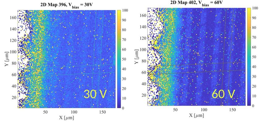
ARCADIA (INFN CSNV Call Project)
    Advanced Readout CMOS Architectures with Depleted Integrated sensor Arrays

                         INFN - Bologna, Milano, Padova, Perugia, Pavia, TIFPA, Torino

       F Alfonsi, G Ambrosi, A Andreazza, S Beolè, M Caccia, A
       Candelori, D Chiappara, T Croci, M Da Rocha Rolo, G-F Dalla
       Betta, A De Angelis, G Dellacasa, N Demaria, B Di Ruzza, A
       Di Salvo, D Falchieri, M Favaro, A Gabrielli, L Gaioni, S
       Garbolino, R A Giampaolo, N Giangiacomi, P Giubilato, R
       Iuppa, M Mandurrino, M Manghisoni, S Mattiazzo, F Nozzoli,
       J Olave, L Pancheri, D Passeri, A Paternò, M Pezzoli, P
       Placidi, L Ratti, E Ricci, S B Ricciarini, A Rivetti, H Roghieh,
       R Santoro, A Scorzoni, L Servoli, F Tosello, G Traversi, C
       Vacchi, R Wheadon, J Wyss, M Zarghami, P Zuccon

        3-year >1M€ R&D project 2019-2021
        Sensor&CMOS design, DAQ, System characterisation (medical, future colliders, space)
2    Andrea Paternò (INFN TO) — andrea.paterno to.infn.it                        3rd FCC Physics and Experiments Workshop, CERN, 2020-01-14
ARCADIA (INFN CSNV Call Project)
    Advanced Readout CMOS Architectures with Depleted Integrated sensor Arrays

    Towards a CMOS sensor design and fabrication platform allowing for:

          Active sensor thickness in the range 50 µm to 500 µm or more

          Operation in full depletion with fast charge collection only by drift

          Small charge collecting electrode for optimal signal-to-noise ratio

          Scalable readout architecture with ultra-low power capability (O(20 mW/cm2))

          Compatibility with standard CMOS fabrication processes: concept study with small-scale
          test structure (SEED), technology demonstration with large area sensors (ARCADIA)

          Use of a deep sub-micron 110nm CMOS node for higher gate density

3    Andrea Paternò (INFN TO) — andrea.paterno to.infn.it                        3rd FCC Physics and Experiments Workshop, CERN, 2020-01-14
SEED - The Sensor

    Two test structures: MATISSE and Pseudo-Matrices

    Technology: 110 nm CMOS CIS technology (quad-well, both PMOS and NMOS), high-resistivity bulk

    Backside: diode surrounded by a guard-ring, custom patterning, process developed with LFoundry

    Process, back-side pattern and geometry validated in silicon (both MATISSE and pseudo-matrices)
4    Andrea Paternò (INFN TO) — andrea.paterno to.infn.it              3rd FCC Physics and Experiments Workshop, CERN, 2020-01-14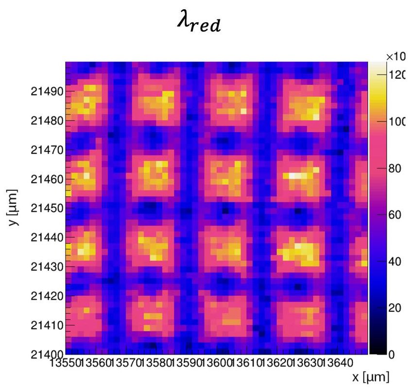
Small-scale demo: MATISSE
                                                                        PIXEL ELECTRONICS
                                                                                         DESIGN
                                                                                                      RESULTS
                                                                                         SPECs
                                                                Technology                  CMOS 110 nm
                                                               Voltage Supply                    1.2 V
                                                               Measurements                  Hit Position
                                                                                             Energy Loss
                                                             Number of Channels                 24 × 24
                                                            Input Dynamic Range              Up to 24 ke-
                                                             Sensor Capacitance           ~10 fF
                                                                 Analog Gain            131 mV/fC 116 mV/fC
                                                           CSA Input Common Mode
                                                                                                    > 600 mV
                                                                   Voltage
                                                               Local Memories                  2 (~70 fF each)
                                                                    Noise                  < 100 e-         ~40 e-
                                                                 Shutter Type                     Snapshot
                                                                                            Correlated Double
                                                               Readout Type
                                                                                                  Sampling
                                                                                              Double Sampling
                                                               Readout Speed                    Up to 5 MHz
                                                               Other Features                Internat test pulse
                                                                                                 Mask Mode
                                                                                            Baseline Regulation
5   Andrea Paternò (INFN TO) — andrea.paterno to.infn.it                        3rd FCC Physics and Experiments Workshop, CERN, 2020-01-14
Small-scale demo: MATISSE

6   Andrea Paternò (INFN TO) — andrea.paterno to.infn.it   3rd FCC Physics and Experiments Workshop, CERN, 2020-01-14
Results in a nutshell: MATISSE
                               Full depletion studies in 100-300-400 µm prototypes

                                                                          Map of pixel reset voltage (MATISSE 24x24
                                                                          pixel matrix, 300µm thickness) as a function
L. Pancheri (TN)

                                                                          of the back-side voltage applied to the sensor.
                                                                          Depletion starts from the back-side.

             7     Andrea Paternò (INFN TO) — andrea.paterno to.infn.it                        3rd FCC Physics and Experiments Workshop, CERN, 2020-01-14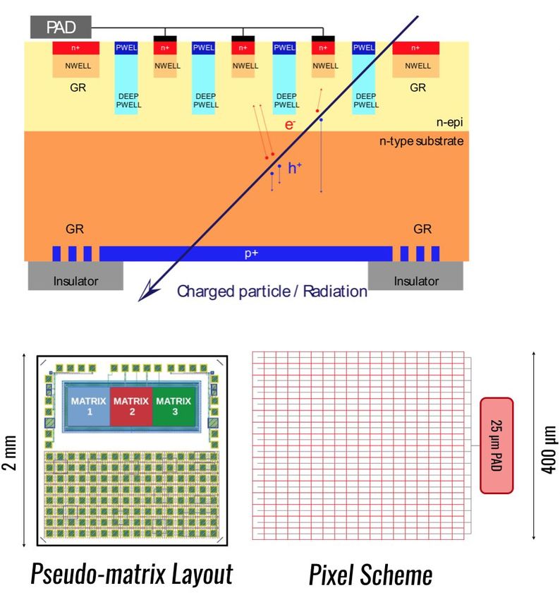
Results in a nutshell: MATISSE
    Preliminary results with 55Fe                                                  Preliminary results with Lasers
       The 55Fe emits monochromatic X-rays at 5.9 keV (Kα). A Kβ line at 6.5 keV
       is also emitted with a relative probability below 5%.

                                                             ADC1   6.5 keV
                                                                  ≈
                                                             ADC2   5.9 keV

8     Andrea Paternò (INFN TO) — andrea.paterno to.infn.it                             3rd FCC Physics and Experiments Workshop, CERN, 2020-01-14
Small-scale demo: Pseudo-Matrices

                                                           Sensor thicknesses: 100 µm, 300 µm, 400 µm

                                                           Three matrices with different pixel sizes: 10 µm
                                                           (40 x 45), 25 µm (16 x 18) and 50 µm (8 x 9)

                                                           Front-side deep-pwell, would host the CMOS
                                                           electronics (no electronics on PMs)

                                                           All the collector nodes of a matrix are shorted
                                                           and connected to a PAD

                                                           Each pixel is shorted using Al metal lines of
                                                           increasing width per PM: 6, 8 and 15 µm

9   Andrea Paternò (INFN TO) — andrea.paterno to.infn.it                  3rd FCC Physics and Experiments Workshop, CERN, 2020-01-14
Results in a nutshell: Pseudo-Matrices
 Cuts along the Metal + P and Metal + N lines on the energy map with               (RUĐER BOŠKOVIĆ INSTITUTE)* Zagreb, Croatia
 varying bias voltages show uniform Charge Collection Efficiency                   600 keV to 2 MeV Tandetron
 above Full Depletion with ~1.7 % loss over metals (100 µm thick)                  TANDEM 1-6 MeV proton source
                                                                                   LASER TCT laboratory

                                                                                                     TCT Scan: CCE

     Standard deviation maps show the expected higher electronic noise when
     the sensor is not depleted (below 30 V), due to the higher top capacitance.

                                                                                                   TCT Scan: Amplitude

10       Andrea Paternò (INFN TO) — andrea.paterno to.infn.it                                       3rd FCC Physics and Experiments Workshop, CERN, 2020-01-14
ARCADIA - Requirements
Apply the experience developed with SEED to a versatile, full-chip prototype
Targeting most stringent requirements for a number of applications:
Low power→ O(20 mW cm−2)
Scale down to O(10 mW cm−2) in Ultra Low Power mode
Small pixel pitch → 25 × 25 μm2
Thin sensors → 100μm
Scalability to large area → up to 4 × 4 cm2
High particle rate→ up to 100 MHz cm−2
Timing resolution → O(1μs) (lower bound due to analog power)
Investigating more advanced solutions for O(10 ns) timing
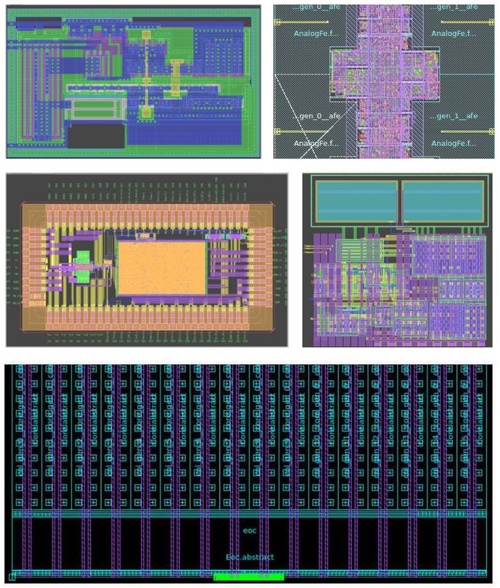
11 Andrea Paternò (INFN TO) — andrea.paterno to.infn.it 3rd FCC Physics and Experiments Workshop, CERN, 2020-01-14ARCADIA - Floorplan 12.8mm
T Padf ame f A al g deb g a d P e a al i
C l m
32 512 i el
12.8mm
Ma i
512 512 i el
16 C l m Bia Cell
16 EOC 0.1mm
Pe i he / 16 8b10b & Se iali e
Padf ame & T a mi e /Recei e
Pixel size 25 µm x 25 µm: process, back-side pattern and geometry validated in silicon (both
MATISSE and pseudo-matrices, electrical, laser, radioactive source and microbeam)
Matrix core 512 x 512, “side-abuttable” to accomodate a 1024 x 512 active area (2.56 x 1.28 cm2).
Matrix and EoC architecture, data links and payload ID: scalable to 2048 x 2048 pixels(1)
Triggerless, binary data readout, event rate up to 100 MHz cm-2
(1) 1D and 2D stitching available at LFoundry
12 Andrea Paternò (INFN TO) — andrea.paterno to.infn.it 3rd FCC Physics and Experiments Workshop, CERN, 2020-01-14ARCADIA - Design
512 32 2
pi els pi els pi els
Pi el Region 0
Core Col mn 15
Pi el Region 1
Core Col mn 0
Core Col mn 1
Core Col mn 2
Analog FEs
512
Col mn 15
Analog FEs
Col mn 0
Col mn 1
Col mn 2
Ma ri
pi els
Pi el Region M
Peripher Inp B ffers and
O p Logic
Chip Ma ri Col mn Core
Matrix (512 x 512) are partitioned into Columns (32 x 512), which are independently read out and
have a dedicated Serializer and LVDS link
Columns are in turn composed of 16 Core Columns (2 x 512) arranged as double pixel columns
Each Core Column stacks 16 Cores (2 x 32), which are the minimum synthesizable unit in the Matrix
Pixel Regions (2 x 4) propagate their output to the periphery, bypassing inactive Cores
13 Andrea Paternò (INFN TO) — andrea.paterno to.infn.it 3rd FCC Physics and Experiments Workshop, CERN, 2020-01-14ARCADIA - Smart Clustering Readout
2 × 4 pixel Regions, logically divided into a
Ma e Ma e Sla e Master (2 x 2) and a Slave (2 x 2)
0 0 0
If Ma e 0 i hi
Try to read out clusters in as few data packets
Sla e as possible
0
Slaves (w/o readout) choose a Master to
Ma e Ma e Sla e attach to (its own, or the following)
1 1 0
If bo h Ma e 0 and Masters propagate 2 × 4 pixel data packet to
Sla e1 a e no hi
Sla e periphery and await Acknowledge pulse
1
Significant reduction of column occupancy and
readout clock
14 Andrea Paternò (INFN TO) — andrea.paterno to.infn.it 3rd FCC Physics and Experiments Workshop, CERN, 2020-01-14ARCADIA - Smart Clustering Readout
Ma e Regi S a e Regi
Hi
ig
ig
A ai ab e
T e
A
A
T
T
T
OR
Se ec ed
OR
S a db
A ai ab e
A ig
Hi
A ig
T
B
B
Both the Smart Clustering and the Token selection mechanism use combinatorial logic
Multiplexers select the data to propagate based on Bottom and Top Assign
15 Andrea Paternò (INFN TO) — andrea.paterno to.infn.it 3rd FCC Physics and Experiments Workshop, CERN, 2020-01-14ARCADIA - Readout performance
w/ Smart Clustering w/o Smart Clustering
Event Rate 100 MHz cm-2
Matches 99,778% 99,712%
Ghost 0,004% 0,08%
Duplicate 0,11% 0,02%
Column Packet rate 15,7 MPps 19,9 MPps
Column bandwidth 443,11 Mbps 510,18 Mbps
Smart Clustering reduces Column BW of 67Mbps!
PRELIMINARY Pixel consumption per pixel, w/ Smart Clustering:
• 10.8 mW cm−2 @100 MHz cm−2
• 7.9 mW cm−2 @10 MHz cm−2
16 Andrea Paternò (INFN TO) — andrea.paterno to.infn.it 3rd FCC Physics and Experiments Workshop, CERN, 2020-01-14ARCADIA - 2048-pix Column Timing
Distance between buffers (um)
25600 1024 512 341 256 204
50
BUF_X1
BUF_X2
45 BUF_X4
BUF_X8
BUF_X16
40 BUF_X20
Propagation delay (ns)
35
30
25
20
15
10
5
0 50 100 150 200 250
Number of buffers
Signals best propagated with repeaters every ~64 pixels (1.6mm) with BUF_X4/BUF_X8
Does not take into account internal propagation to sink! Conservative measurement
ARCADIA has signal repeaters every 800um in its 512-pix column (12.8mm tall)
Achieve ~12.5ns propagation delay on a 2048-pix Column
17 Andrea Paternò (INFN TO) — andrea.paterno to.infn.it 3rd FCC Physics and Experiments Workshop, CERN, 2020-01-14ARCADIA - Peripheral Dataflow
H g Ra e de L Ra e de
C
C
C
C
C
C
C
C
C
C
15
15
0
1
2
...
0
1
2
...
TX TX TX TX TX TX TX TX TX TX
Each Column (32x512 pixels) has a readout BW of 443Mbps
Link is DC-balanced via 8b10b encoding, which increase BW to 553Mbps
Column data is sent out via dedicated 320MHz DDR Serializers
For space applications, which has very low hit rates, the packets from all the columns are
sent via a single serializer, while the others are turned off along with their LVDS links.
18 Andrea Paternò (INFN TO) — andrea.paterno to.infn.it 3rd FCC Physics and Experiments Workshop, CERN, 2020-01-14ARCADIA: ongoing activities
01/2019 01/2022
TCAD 2D/3D sensor simulation: geometry, p-well spacing, node capacitance, transient
CMOS Analogue IP block design: continuous and discrete-time VFE design; 12-bit SAR ADC IP-core,
custom LVDS Tx/Rx: LF11is prototyping run September 2019
CMOS Digital IP block design and Chip Integration:
SPI and Serialiser (8b/10b) soft-IP Cores 110nm ready
Full matrix integration ready, periphery ongoing
Data acquisition: started development of DAQ for the full-chip
Characterisation: laser and microbeam tests with 100-300 µm
pseudo-matrices @RBI (Zagreb), tests with Fe55, new laser test setup (spot size 8 µm) under construction
1st engineering run (dedicated front/back-side maskset): mid-2020
19 Andrea Paternò (INFN TO) — andrea.paterno to.infn.it 3rd FCC Physics and Experiments Workshop, CERN, 2020-01-14Progress on Arcadia
F Alfonsi, G Ambrosi, A Andreazza, S Beolè, M Caccia, A Candelori, D Chiappara, T Croci, M Da Rocha Rolo,
G-F Dalla Betta, A De Angelis, G Dellacasa, N Demaria, B Di Ruzza, A Di Salvo, D Falchieri, M Favaro, A
Gabrielli, L Gaioni, S Garbolino, R A Giampaolo, N Giangiacomi, P Giubilato, R Iuppa, M Mandurrino, M
Manghisoni, S Mattiazzo, F Nozzoli, J Olave, L Pancheri, D Passeri, A Paternò, M Pezzoli, P Placidi, L Ratti, E
Ricci, S B Ricciarini, A Rivetti, H Roghieh, R Santoro, A Scorzoni, L Servoli, F Tosello, G Traversi, C Vacchi, R
Wheadon, J Wyss, M Zarghami, P Zuccon
Thank You for your time !You can also read