Tungsten-Carbon Nanotube Composite Photonic Crystals as Thermally Stable Spectral-Selective Absorbers and Emitters for Thermophotovoltaics - Sites ...
←
→
Page content transcription
If your browser does not render page correctly, please read the page content below

Communication
Energy Harvesting                                                                                                           www.advenergymat.de

Tungsten–Carbon Nanotube Composite Photonic Crystals
as Thermally Stable Spectral-Selective Absorbers and
Emitters for Thermophotovoltaics
Kehang Cui,* Paul Lemaire, Hangbo Zhao, Timothy Savas, Gregory Parsons,
and A. John Hart*

                                                                                                  Materials with controlled photon absorp-
Thermophotovoltaics (TPVs) is a promising energy conversion technology                            tion and thermal emission have wide
which can harvest wide-spectrum thermal radiation. However, the                                   application in the fields of energy-effi-
                                                                                                  cient lighting,[1–3] molecular sensing,[4–7]
manufacturing complexity and thermal instability of the nanophotonic
                                                                                                  radiative cooling,[8–10] and energy har-
absorber and emitter, which are key components of TPV devices,                                    vesting.[11–15] Thermophotovoltaic (TPV)
significantly limit their scalability and practical deployment. Here,                             systems[16] rely on PhC surfaces to convert
tungsten–carbon nanotube (W-CNT) composite photonic crystals                                      broad-band solar irradiation or combus-
(PhCs) exhibiting outstanding spectral and angular selectivity of photon                          tion heat to narrow-band near infrared
absorbance and thermal emission are presented. The W-CNT PhCs are                                 thermal emission which matches the
                                                                                                  electronic bandgaps of photovoltaic (PV)
fabricated by nanoscale holographic interferometry-based patterning
                                                                                                  cells. By harvesting sub-bandgap photons
of a thin-film catalyst, modulated chemical vapor deposition synthesis                            and hot carriers, TPVs can exceed the
of high-density CNT forest nanostructures, and infiltration of the CNT                            Shockley–Queisser (SQ) efficiency limit[17]
forests with tungsten via atomic layer deposition. Owing to their highly                          and have output energy density as high as
stable structure and composition, the W-CNT PhCs exhibit negligible                               105 W m−2.[18]
degradation of optical properties after annealing for 168 hours at 1273 K,                           Use of engineered nanophotonic
                                                                                                  surfaces as absorbers and emitters has sig-
which exceeds all previously reported high-temperature PhCs. Using                                nificantly improved the power conversion
the measured spectral properties of the W-CNT PhCs, the system                                    efficiencies of TPV devices from below
efficiency of a GaSb-based solar TPV (STPV) that surpasses the                                    1% to 6.7%.[12,13,18,19] However, the experi-
Shockley–Queisser efficiency limit at modest operating temperatures                               mentally demonstrated efficiencies of TPV
and input powers is numerically predicted. These findings encourage                               systems are still far below their theoretical
                                                                                                  capability, in large part due to parasitic
further practical development of STPVs, and this scalable fabrication
                                                                                                  thermal losses.[12,13,19] Absorbers and emit-
method for composite nanostructures could find other applications in                              ters for TPVs are usually manufactured
electromagnetic metamaterials.                                                                    by deep reactive ion etching or scanning
                                                                                                  electron beam lithography, requiring clean
                                                                                                  room facilities and expensive equipment
                                                                                                  which limits the practical device area.[20]
                                                                             Recent studies have demonstrated absorbers and emitters fab-
Dr. K. Cui, Dr. H. Zhao, Prof. A. J. Hart
Department of Mechanical Engineering and Laboratory
                                                                             ricated by nanoimprint lithography,[21] nanopyramid template
for Manufacturing and Productivity                                           stripping,[22] nanoparticle dewetting,[23] and self-assembled
Massachusetts Institute of Technology                                        reverse opal methods.[24] All of these techniques are intrinsi-
Cambridge, MA 02139, USA                                                     cally more scalable than lithography-based patterning, but
E-mail: cuik@mit.edu; ajhart@mit.edu                                         cannot replicate the precision of the latter, thereby sacrificing
Dr. P. Lemaire, Prof. G. Parsons                                             optical selectivity.
Department of Chemical and Biomolecular Engineering
North Carolina State University                                                 Maintaining the submicron characteristic dimensions of
Raleigh, NC 27606, USA                                                       PhCs at high operating temperatures (>800 °C) over a long
Dr. T. Savas                                                                 duration is another technological difficulty. For 1D super-
Research Laboratory of Electronics                                           lattice PhCs, a slight mismatch in the thermal expansion
Massachusetts Institute of Technology                                        coefficient between layers can cause delamination due to ther-
Cambridge, MA 02139, USA
                                                                             momechanical stress.[25–27] Refractory metals typically used in
      The ORCID identification number(s) for the author(s) of this article   2D and 3D PhCs (e.g., tungsten, ruthenium, and tantalum)
      can be found under https://doi.org/10.1002/aenm.201801471.
                                                                             suffer from surface diffusion and structural degradation at
DOI: 10.1002/aenm.201801471                                                  high operating temperatures,[28] causing losses of selectivity

Adv. Energy Mater. 2018, 8, 1801471                               1801471 (1 of 9)              © 2018 WILEY-VCH Verlag GmbH & Co. KGaA, Weinheim
www.advancedsciencenews.com                                                                                                     www.advenergymat.de

Figure 1. Design of W-CNT PhCs. a) Spectral selectivity of ideal absorber and emitter for STPV system. Inset: schematic of geometric parameters (perio-
dicity a, nanocavity diameter d, and thickness t) of the W-CNT PhCs that determine the spectral selectivity, and schematic of the W-CNT composite
material. b) UV–vis–NIR reflection spectra of the top surface of the unpatterned W-CNT composite and the W thin film sputter-deposited on a polished
Si/SiO2 substrate. Inset: SEM images of the top surface and the sidewall of the unpatterned W-CNT composite. c,d) Numerical optimization of the
spectral cutoffs of the absorber and emitter. e,f) Numerical optimization of the periodicity a and nanocavity diameter d for the design of the W-CNT
nanophotonic absorber and emitter.

in photon absorption and thermal emission. Coatings such                     CVD process, as compared in Figure S1 of the Supporting
as HfO2[24,29–32] can enhance thermal stability, yet elemental               Information. The surface of the reference low-density VACNTs
scarcity and high cost potentially prevent their use at scale.[33,34]        is a blackbody absorbing light omnidirectionally, similar to
   Here we propose a scalable approach for the fabrication of                previous studies,[35,36] while the surface of the HD-VACNTs is
PhCs for use in TPV systems, via formation of tungsten–carbon                shiny and reflective (Figure S1c,d, Supporting Information).
nanotube (W-CNT) composite surfaces having high spectral                     UV–vis–NIR reflection spectra (Figure S1e, Supporting Infor-
selectivity and exceptional thermal stability. The W-CNT PhCs                mation) demonstrate that the reflectivity of the top surface of
are designed to function as the selective absorber and emitter               the HD-VACNTs (≈0.2) is ≈100-fold greater than that of the
in a standard solar thermophotovoltaic (STPV) system using an                reference VACNTs, and is similar to that of graphite[37] and
external GaSb PV cell (bandgap 0.7 eV). As shown in Figure 1a,               glassy carbon.[38–41]
both the absorber and emitter have spectral cutoffs, together                   After HD-VACNT growth, the W-CNT composite material
serving as a thermal rectifier. In a STPV system, the absorber               is formed by atomic layer deposition (ALD) of ≈2 nm thick
ideally converts full-spectrum solar irradiation to thermal                  Al2O3 and ≈20 nm thick W onto the CNTs. The SEM images
energy with unity absorbance, and serves as a thermal insula-                in the insets of Figure 1b demonstrate that the top surface of
tion layer for the emitter to guarantee unidirectional thermal               the W-CNT composite is smooth and solid, while the side-
emission to the PV cell below. An ideal emitter then quenches                wall is composed of Al2O3-coated CNTs embedded in the W
the radiation below the bandgap of the PV cell (zero emittance)              matrix. To examine the validity of the W-CNT composite mate-
and enhances the thermal emission elsewhere (unity                           rial for the fabrication of 2D PhCs, UV–vis–NIR spectra of a
emittance). The spectral selectivity of the absorber and emitter             sputtered W thin film and the top surface of the unpatterned
can be tailored via the nanocavity diameter d, periodicity a and             W-CNT composite are compared (Figure 1b), and match well
thickness t (Figure 1a).                                                     with each other in the visible and NIR ranges. The top surface
   Our approach is to use nanopatterned vertically aligned                   of the unpatterned W-CNT composite has even greater absorp-
carbon nanotubes (VACNTs) as a nanoporous scaffold for                       tivity below 400 nm, which may be attributed to roughness-
infiltration of a refractory metal (W), forming thermally stable             induced Mie scattering.
composite PhCs. Uniform, high-density CNT growth is critical                    Design of the W-CNT nanophotonic absorber and emitter for
to achieve submicron VACNT features and form precise PhC                     the STPV system has two main steps: 1) optimization of the
scaffolds. A dynamic chemical vapor deposition (CVD) process                 spectral cutoff position, and 2) optimization of the geometric
with carbon pre-conditioning of the catalyst (see the Experi-                parameters (d, a, and t) of the W-CNT PhCs to maximize the
mental Section) was used to grow VACNTs with much higher                     absorber and emitter figures of merit. The absorber figure of
density and alignment (HD-VACNTs) than the conventional                      merit (ηabsorber) is defined as the ratio of the stored thermal

Adv. Energy Mater. 2018, 8, 1801471                               1801471 (2 of 9)                 © 2018 WILEY-VCH Verlag GmbH & Co. KGaA, Weinheim
www.advancedsciencenews.com www.advenergymat.de
energy to the total solar irradiance multiplied by the Carnot are subsequently optimized. The d/a of the nanocavities in
efficiency the W-CNT nanophotonic absorber and emitter are chosen to
be 480/600 nm and 640/900 nm, respectively, giving ηabsorber
T and ηemitter both greater than 80%, as shown in Figure 1e,f.
ηabsorber = 1 − C ∫ d λα ( λ )I s ( λ ) − ∫ d λα ( λ ) I BB ( λ ,T ) / C ∫ d λI s ( λ )
Ta solar BB solar To realize the W-CNT PhCs according to our computational
(1) design, nanopatterned CNTs are grown from supported cata-
lyst films (Fe/Al2O3) patterned by holographic interferometry
where C is the number of suns, λ is the wavelength, Is is the (see the Experimental Section), followed by ALD coating with
solar irradiance, IBB is the blackbody radiation, Ta is the Al2O3 and W, resulting in uniform, high aspect ratio composite
ambient temperature (300 K), and α is the spectral absorbance of PhCs with precise nanocavity dimensions. The process is sche-
the absorber. The emitter figure of merit (ηemitter) is the ratio of matically depicted in Figure 2a. For CNT synthesis, the sub-
the energy contained in the electron-hole pairs in the PV cell to strate with the nanopatterned catalyst film is rapidly inserted
the total thermal energy irradiated from the emitter, given by to the CVD reactor using an automated mechanism after the
furnace reaches the target temperature and stable atmosphere
∞ ∞
Eg (C2H4/He/H2O/H2); under these conditions, the CNTs grow
ηemitter = ∫ dEε (E ) I BB (E ,T ) / ∫ dEε (E ) I BB (E ,T ) (2) rapidly (≈2 µm s−1), and the final CNT thickness of 15 µm is
Eg E 0
controlled by withdrawing the substrate from the reactor at a set
where ε is the spectral emittance of the emitter, E is photon time. Next, Al2O3 and W coatings are sequentially deposited by
energy, and Eg is the bandgap of the GaSb cell, i.e., 0.7 eV. The ALD. For Al2O3, use of ozone as the oxidizing agent[46,47] causes
spectral cutoff positions are optimized using step function-like uniform adsorption of the organometallic precursor (trimethy-
absorbance and emittance laluminum, TMA), resulting in a thin, conformal Al2O3 coating
which subsequently serves as a seed layer for W deposition.
0.95; λ ≤ λcutoff The result is a uniform composite PhC with the nanopatterned
α p ,ε p ( λ ) = (3)
0.05; λ > λcutoff VACNTs embedded in a nanocrystalline W matrix.
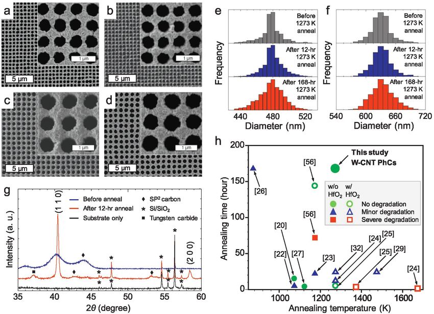
As shown in Figure 2b,c, the diameter and periodicity of
where αp and εp respectively denote the absorbance and the nanocavities in the as-grown nanopatterned VACNTs for
emittance, and λcutoff is the cutoff wavelength. The values the W-CNT nanophotonic absorber and emitter are highly uni-
0.95 and 0.05 adopted here are based on the highest form, measuring 524 ± 12 and 602 ± 13 nm as well as 675 ± 11
αp, εp(λ ≤ λcutoff) and lowest αp, εp(λ > λcutoff) among previous and 894 ± 14 nm, respectively. The VACNT wall thickness
studies.[15,19,20,22,24,26,29,32,42,43] between adjacent cylindrical nanocavities is only 78 ± 10 nm,
The calculated values of ηabsorber versus the spectral cutoff which to our knowledge is the smallest freestanding CNT
and STPV working temperature (under 100 suns illumination) forest structure reported in literature to date.[48–50] At the
are shown in Figure 1c. The maximum ηabsorber of 75.6% is thickness of 15 µm, the walls between nanocavities reach an
predicted at a cutoff position of 1171 nm and operating tem- aspect ratio (AR) of ≈200, in only 10 s of CVD synthesis after
perature of 1400 K. The optimal cutoff position is dictated by insertion of the substrate to the heated reactor. High-aspect
the tradeoff between solar absorption and thermal emission at ratio metal-based PhCs fabricated by top-down processes are
operating temperature. For the emitter, a spectral cutoff posi- challenged by inevitable sidewall undercutting in anisotropic
tion of 1673 nm (Figure 1d) is chosen to match the electronic etching,[51,52] which in literature are limited to 8 µm.[53–56]
bandgap of GaSb PV cells (0.7 eV). At this cutoff position, SEM images show that the nanocavity diameters of the
ηemitter reaches the maximum value for each operating tempera- W-CNT absorber (479 ± 17 nm) and emitter (633 ± 19 nm) are
ture from 1000 to 2000 K. uniform through the thickness.
Next, the W-CNT PhCs were designed to realize the desired As shown by the UV–vis–NIR spectra in Figure 3a, the
spectral cutoffs calculated above, using a finite-difference time W-CNT nanophotonic absorber has a sharp spectral cutoff
domain method (FDTD, incorporated via the MIT Electromag- at 1130 nm (1.1 eV), and near-unity absorbance is observed
netic Equation Propagation (MEEP) package.[44] The material above 1.2 eV. The W-CNT nanophotonic emitter exhibits a
dispersion was extracted from the data in Figure 1b using the steep spectral cutoff at 1600 nm and near-unity emittance
Lorentz–Drude model (see the Experimental Section). The effect below 1300 nm (Figure 3b). The measured cutoff frequencies
of the thickness t on the spectral selectivity of two representa- generally match the corresponding FDTD numerical simula-
tive PhC designs (a = 1.3, d = 1.1 µm; and a = 1.1, d = 0.9 µm, tions, but the experimental values of the absorbance and emit-
chosen from ref. [15]) is shown in Figure S2 of the Supporting tance are slightly higher than the simulation results over the
Information. When the thickness increases from 2 to 12 µm, whole spectral range, likely owing to diffuse reflection from
the absorbance/emittance at the wavelengths below the spectral the top surface.[26] Greater absorbance and emittance in the
cutoff is enhanced significantly. This is because the increased longer wavelength range cause more re-emission to the envi-
PhC thickness reduces photon transmission and increases ronment and sub-bandgap photon emission to the PV cell,
photon-nanocavity interaction time to realize cavity resonator which would decrease the STPV system efficiency. This could
modes.[43,45] However, further increasing the thickness be mitigated by surface polishing[57–59] or further modification
to 15 and 20 µm does not appreciably change the absorb- of the CVD process.
ance or emittance for both PhC designs. With the thickness t The efficiency of an STPV system is also influenced by
set as 15 µm, the diameter and periodicity of the nanocavity the incident angle of the thermal emission upon the PV cell.
Adv. Energy Mater. 2018, 8, 1801471 1801471 (3 of 9) © 2018 WILEY-VCH Verlag GmbH & Co. KGaA, Weinheim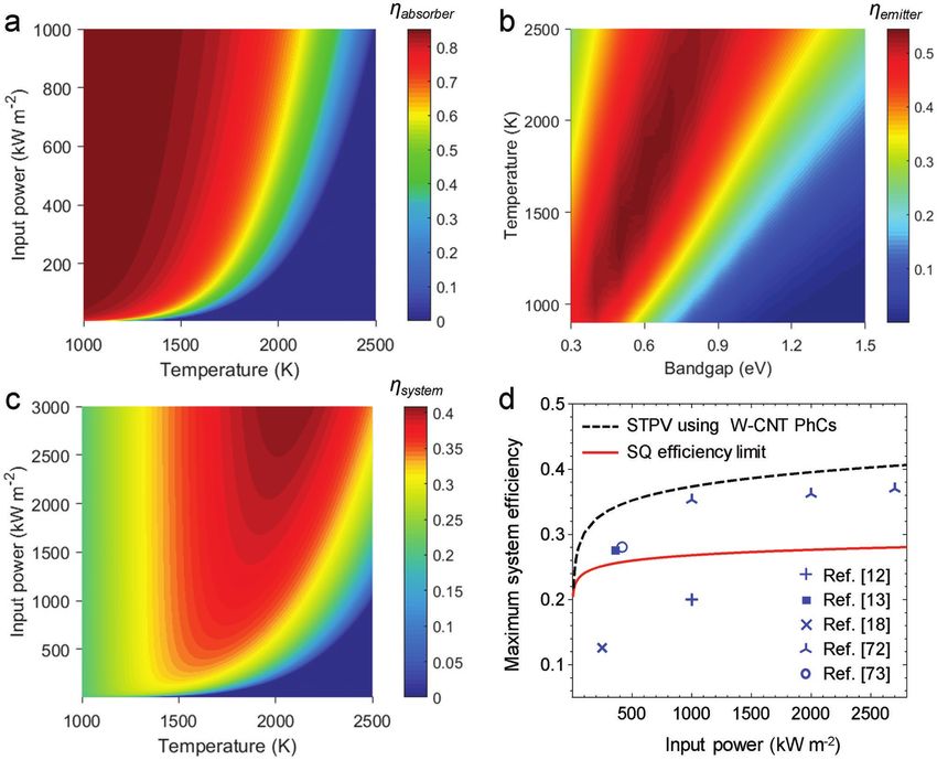
www.advancedsciencenews.com                                                                                                    www.advenergymat.de

Figure 2. Fabrication of W-CNT PhCs. a) Schematic key steps of fabrication process (note the CNTs are shown as parallel and equally spaced to simplify
the depiction at the nanoscale). b,c) Top-view and side-view SEM images of the as-grown nanopatterned VACNT arrays for the W-CNT absorber and
emitter. d,e) Top-view and side-view SEM images of the W-CNT absorber and emitter after ALD coating.

When the thermal emission impinges on the PV cell at oblique                 show no change in the absorber efficiency (ηabsorber = 84%) after
angles, the surface recombination rate of the electron-hole pairs            168 h annealing at 1273 K. The emitter efficiency is relatively
increases,[60–62] resulting in considerable losses in the system             low before annealing (ηemitter = 38.7%) and increases to 50.8%
efficiency and power output density. The angular-dependent                   after annealing (Table S1, Supporting Information). SEM images
absorbance and emittance are measured by UV–vis–NIR                          (Figure 4a–d) show that the edges of the nanocavities remain
spectroscopy, as shown in Figure 3c,d. The average absorbance                sharp after annealing. The nanocavity diameter distributions
and emittance (from 300 to 800 nm) both exceed 0.8 in the                    broaden slightly (Figure 4e,f), but the mean diameters remain
angle range of 0° to 22.5° and decline drastically when the                  unchanged within our measurement error (Table S1, Supporting
incident angle further increases, which is consistent with                   Information). As shown in Figure 4g, after 12 h annealing at
the FDTD simulations (Figure S5, Supporting Information).                    1273 K, the W (1 1 0) peak is slightly shifted, and the full-width
Therefore, we conclude that the W-CNT absorber can provide                   half-maximum (FWHM) of the peak is significantly narrowed.
a 45° acceptance cone for the concentrator design and limit the              This is mainly attributed to the release of microstrain accumu-
radiation loss to the environment outside the acceptance cone.               lated during atomic layer deposition process and a phase transi-
Further, the W-CNT emitter can effectively mitigate nonradia-                tion from the as-deposited nanocrystalline W to alpha-phase (bcc)
tive recombination (Shockley–Read–Hall recombination) in the                 W. After 168 h annealing at 1273 K (Figure S4, Supporting Infor-
PV cell,[60–62] which benefits the power output density of the               mation), the minor narrowing of the FWHM of the W (1 1 0)
STPV system.                                                                 and W (2 0 0) peaks demonstrates a 19.6% reduction of micro-
   The optical and structural stability of PhCs at high tem-                 strain and 3.5% growth of crystallite size, according to the Wil-
peratures is critical to the practical application of STPV sys-              liamson–Hall plot.[64] The increased crystallinity and the denser
tems.[29,31,56,63] In Figure 3a,b, we also illustrate that, after            coating layer result in higher optical reflectivity (metallicity) in
annealing at 1273 K for up to 168 h (10−3 Torr vacuum with He                the near infrared range,[27,65,66] thereby suppressing the thermal
protection), the spectral selectivity does not deteriorate for both the      emission above the spectral cutoffs and improving the overall
W-CNT nanophotonic absorber and emitter. Our measurements                    performance.

Adv. Energy Mater. 2018, 8, 1801471                              1801471 (4 of 9)                 © 2018 WILEY-VCH Verlag GmbH & Co. KGaA, Weinheim
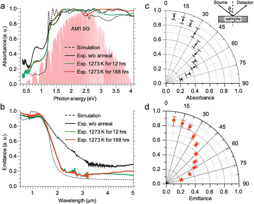
www.advancedsciencenews.com www.advenergymat.de Figure 3. Optical properties of the fabricated W-CNT PhCs. a,b) Spectral absorbance and emittance of the W-CNT nanophotonic absorber and emitter before annealing, and after 12 and 168 h annealing at 1273 K, compared with the corresponding simulation values. c,d) Dependence of the average absorbance and emittance (300–800 nm) on the incidence angles for the W-CNT absorber and emitter. The angle θ is defined at the upper right. The rate of the surface diffusion of metals at elevated tem- a HfO2 protection layer has been widely shown to improve peratures is proportional to the divergence of the gradient of thermal stability of PhCs,[24,25,29,56] concern arises due to the the local mean curvature of the surface.[28,67] For metal-based scarcity and high processing cost of Hf.[33,34] It was clarified by PhCs in prior work, the edges of the nanocavities have the Peykov et al.[28] that the dominant failure mechanism for refrac- largest local mean curvature and hence the highest surface dif- tory metal-based PhCs at high temperature is surface diffusion. fusion velocity. This has resulted in the rounding and collapse The surface diffusion rate of W increases by ≈10 times with of the nanocavity edges, and thus the deterioration of spectral every 200 K increase in temperature. For the W-CNT structure, selectivity at high temperatures.[28,50] In our work, the nanocavi- the effect of local mean curvature could be mitigated because ties in the W-CNT PhCs are realized by infiltration of the nano of support from the CNT scaffold. This makes the thermal sta- patterned CNT forests with W, rather than top-down etching bility of W-CNT PhCs comparably superior to those tested at of a single material. Our approach avoids residual etching higher temperatures. contaminants and process-induced surface defects which are In laboratory-scale STPV modules developed so far,[12,13,19,71] known to degrade surface integrity of W.[68–70] The geometry of the input power and operating temperature have been limited our pattern is intrinsically stable, as the surface diffusion rate below 1000 kW m−2 and 1300 K, respectively. Our results show over the whole W-CNT PhCs is uniform, and the diffusion of promise to enable higher temperature STPV modules. To con- W in between individual Al2O3-coated CNTs is not energetically clude this study, we estimate the power conversion efficiency of favorable. a planar STPV system with the W-CNT nanophotonic absorber In Figure 4h, the thermal stability of the present W-CNT and emitter placed over a GaSb PV cell. A 1D thermal diode PhCs is compared with data from previous studies of PhCs model utilizes the experimentally measured spectral properties made of various materials.[20,22–27,29,32,56] We categorize this of the W-CNT PhCs to predict the STPV system efficiency at comparison according to the degradation of the absorber and input powers (100–3000 kW m−2) and operating temperatures emitter efficiency. Among reported thermal stability tests car- (1000–2500 K). The model neglects the thermal loss from the ried out for longer than 48 h,[26,56] our W-CNT PhCs (without a system support and packaging as well as the resistive loss from protective coating) sustain the highest annealing temperature the PV cell. This assumption is reasonable, because the major (1273 K) without degradation. With HfO2 as the protection loss mechanisms for a large-scale planar STPV system are the layer, planar Ta-W PhCs showed minor degradation after 24 h re-emission from absorber to environment and above-bandgap annealing at 1473 K,[29] while 3D inverse opal W PhCs showed emission from emitter to PV cell.[12,13,19] As shown in Figure 5a, severe degradation after 1 h annealing at 1673 K.[24] Although at modest input powers (
www.advancedsciencenews.com                                                                                                            www.advenergymat.de

Figure 4. Thermal stability of the W-CNT PhCs. SEM images of a,b) the W-CNT nanophotonic absorber and c,d) the W-CNT nanophotonic emitter,
after 12 and 168 h annealing at 1273 K. e,f) Histograms of the nanocavity size distribution of the W-CNT nanophotonic absorber and emitter before
and after annealing at 1273 K, respectively. g) XRD spectra of the W-CNT nanophotonic surface before and after 12 h annealing at 1273 K, using the
Si/SiO2 substrate as reference. h) Comparison of thermal stability of the W-CNT PhCs to previously reported PhCs: ref. [20] TiN, ref. [22] Ni-Al2O3,
ref. [23] Au-Al2O3, refs. [24,25] W-HfO2, ref. [26] W-Ni-YSZ, ref. [27] W-Al2O3, ref. [29] Ta-W-HfO2, Ref. [32] Ru-HfO2, and ref. [56] Ta-HfO2. No degradation,
minor degradation, and severe degradation denote 0–5%, 5–15%, and greater than 15% degradation of absorber/emitter efficiency, respectively.

at relatively low operating temperatures (1000–1400 K).                          performance is especially superior at lower input powers
Figure 5b shows the operating temperature at which ηemitter is                   (1000 kW m−2), we predict slightly
W-CNT nanophotonic absorber and emitter pair are promising                       higher maximum system efficiency than a published model
as a thermal rectifier between the Sun and the PV cell at the                    using tungsten pyramid nanostructures as the absorber and
thermally stable temperature (1273 K).                                           emitter.[72] By utilizing additional rugate filters,[13,74] the STPV
   The STPV system efficiency (ηsystem) is a product of ηabsorber,               system efficiency could be further improved.
ηemitter as well as the correction factors of the PV cell.[72] Figure 5c            In summary, we have explored a new W-CNT composite
shows at the thermally stable operating temperature (1273 K),                    material for 2D PhCs. The fabricated W-CNT PhCs exhibit
the predicted efficiency of the STPV system exceeds the SQ                       excellent spectral and angular selectivity as well as out-
efficiency limit of the PV cell (23%) under a modest input                       standing thermal stability after high-temperature annealing.
power of 100 kW m−2, and reaches as high as 33% under an                         Importantly, our process is intrinsically scalable; holographic
input power of 1000 kW m−2. Simultaneously increasing the                        interferometry can be performed with simple optical setup
input power to 3000 kW m−2 and operating temperature to                          in the ambient; both CNT growth and ALD are vapor-phase
2000 K results in an increase of ηsystem to 41%. However, higher                 processes which can be deployed in a roll-to-roll fashion; and
input power and operating temperature would increase the                         no conventional masks or scanning lithography methods
cost and thermal loss, respectively, which would counteract the                  are required. Therefore, beyond STPV systems, CNT-based
moderate improvement. Therefore, while scientifically inter-                     composite nanophotonic surfaces are also promising to be
esting, we feel the pursuit of even higher-temperature thermal                   applied in other high-temperature energy conversion devices,
stability of the W-CNT PhCs not necessary for practical imple-                   such as photothermionic energy converters,[75] solar thermo-
mentation of our technology.                                                     electric converters,[76] and thermophotonic solar cells.[77] In
   The predicted maximum efficiency of the STPV system                           addition, the general strategy of nanopatterned CNT growth
with the W-CNT nanophotonic absorber and emitter are                             followed by vapor-phase infiltration of a solid matrix may
compared with prior estimates using different absorbers and                      be applied to engineer electromagnetic metasurfaces for a
emitters,[12,13,18,72,73] as shown in Figure 5d. Our predicted                   variety of needs.

Adv. Energy Mater. 2018, 8, 1801471                                  1801471 (6 of 9)                   © 2018 WILEY-VCH Verlag GmbH & Co. KGaA, Weinheim
www.advancedsciencenews.com                                                                                                        www.advenergymat.de

Figure 5. Simulated performance of a STPV system incorporating the measured spectral properties of the W-CNT absorber and emitter. a) Absorber
efficiency of the STPV system versus solar input power and operating temperature. b) Emitter efficiency of the STPV system versus PV bandgap and
operating temperature. c) Predicted STPV system efficiency versus solar input power and operating temperature. d) Predicted maximum STPV system
efficiency, compared to the SQ efficiency limit, and to the predicted maximum system efficiencies using: refs. [12,13] VACNT as the absorber and
multilayer Si/SiO2 as the emitter, ref. [18] Ta-HfO2 PhCs as the absorber and emitter, ref. [72] tungsten pyramid nanostructures as the absorber and
emitter, and ref. [73] liquid Si as the absorber and liquid Sn as the emitter.

Experimental Section                                                          at 750 °C, a transfer arm carrying a Si/SiO2 substrate loaded with the
                                                                              catalysts was inserted into the hot chamber with 400 sccm H2 and
   CNT Catalyst Deposition: The catalyst composed of Fe (1 nm) upon           100 sccm dry He (99.999%, Airgas). After annealing at 750 °C for
Al2O3 (10 nm) was deposited by electron beam evaporation (VES-2550,           10 min, the substrate was retracted from the hot chamber to cool down.
Temescal) on a Si wafer (0.5 mm) with a thermally grown oxide layer           The precursors—100 sccm C2H4, 200 sccm H2, 200 sccm wet He, and
(200 nm).                                                                     800 sccm dry He—were then introduced into the hot chamber. The
   Catalyst Nanopatterning Using Nanoscale Holographic Interferometry: A      substrate was inserted again after the stabilization of the precursor flow
bilayer stack of a bottom anti-reflection coating (BARC, Brewer Science       (≈5 min) for the synthesis of the HD-VACNTs. The typical growth rate of
XHRi-16) and a negative photoresist layer (Futurrex NR7-250) was spin-        the CNT array was 2 µm s−1. After reaching the desired CNT thickness,
coated on the catalyst-coated Si substrate, followed by baking at 180 °C      the growth was terminated by withdrawing the substrate from the
for 1 min. The bilayer stack was exposed to the HeCd laser using a            reactor using the transfer arm under dry He purge.
Lloyd’s mirror setup (Figure S3, Supporting Information). The periodicity        Atomic Layer Deposition: Before the metallic tungsten ALD process, a
of the nanopattern is given by (λ/2)/sin(θ/2), where λ = 325 nm is the        2 nm thick and conformal Al2O3 layer was deposited on the CNT arrays
HeCd laser wavelength, and θ is the angle of the Lloyd’s mirror. The          by 30 cycles of ALD (Gemstar XT, Arradiance Corporation) using ozone
achievable periodicity range is from ≈175 to ≈1500 nm. The pattern            (generated by Pacific Ozone, using O2 99.999% purity from Airgas) and
was then developed by immersion of the substrate in the mixture               TMA (98% purity, STREM Chemicals) as precursors. The Al2O3 deposition
of tetramethylammonium hydroxide (Futurrex RD-6) and water with               rate was ≈0.06 nm per cycle. The W ALD process was performed in a
volume ratio of 3:1 for 40 s. The exposed BARC and catalyst layers            home-built flow tube reactor at 220 °C, with an inert Ar carrier flow rate of
were sequentially removed by He-O2 (20%) RF plasma dry etching                210 sccm, to produce a baseline pressure of 1.5 Torr.[80] The W ALD
(Plasma-Therm, 200 W, 7 mTorr) for 2 min and immersion in 1 m NaOH            process (35 cycles) was realized by alternately exposing the Al2O3-coated
for 1 min. A scotch tape was then applied and exfoliated manually to          CNT arrays to diluted WF6 (99.9%, Sigma-Aldrich) and SiH4. The SiH4 was
remove the residues and contaminants.                                         a dilute mixture (2% by weight) in 99.999% Ar (Custom Gas Solutions).
   Synthesis of High-Density VACNTs: The HD-VACNTs were synthesized           The carrier and purge gas was 99.999% pure N2, and it passed through
using a carbon preconditioning dynamic CVD process. The CVD                   an inert gas purifier (Entegris GateKeeper) to remove residual water
system was fully automated with an in situ monitoring camera, i.e.,           before entering the reactor. Typical precursor exposures in Langmuir
Robofurnace.[78,79] A thin layer of carbon was first deposited on the inner   (1 L = 10−6 Torr s) were ≈6 × 10⁵ Langmuir, 5 × 10⁵ Langmuir, and
wall of the CVD chamber at 750 °C by the flow mixture of 100 sccm C2H4        1 × 10⁷ Langmuir for SiH4, WF6, and Ar, respectively. The W deposition
(99.9%, Airgas), 200 sccm H2 (99.999%, Airgas), and 400 sccm wet He           rate was ≈0.5–1 nm per cycle. Then, the as-deposited W-CNT composites
(100 ppm H2O) for 5 min. With the system temperature maintained               were annealed at 1073 K for 1 h to help densify and stabilize W.

Adv. Energy Mater. 2018, 8, 1801471                                1801471 (7 of 9)                 © 2018 WILEY-VCH Verlag GmbH & Co. KGaA, Weinheim
www.advancedsciencenews.com www.advenergymat.de
Annealing: The W-CNT samples were annealed in a tube furnace [1] J. Zhou, X. Chen, L. J. Guo, Adv. Mater. 2016, 28, 3017.
(Carbolite 3-zone furnace). Before annealing, the quartz tube was fully [2] O. Ilic, P. Bermel, G. Chen, J. D. Joannopoulos, I. Celanovic,
evacuated and re-charged with He (99.999%, Airgas), and repeated for M. Soljačić, Nat. Nanotechnol. 2016, 11, 320.
three time to remove residue oxygen and water (below 0.1 ppm). The [3] J.-J. Greffet, R. Carminati, K. Joulain, J.-P. Mulet, S. Mainguy,
furnace was heated at a rate of 200 degree Celcius/hour until the target Y. Chen, Nature 2002, 416, 61.
temperature with 150 sccm He flow, under a pressure below 10−3 Torr. [4] Z. Xie, K. Cao, Y. Zhao, L. Bai, H. Gu, H. Xu, Z.-Z. Gu, Adv. Mater.
After annealing, the samples were cooled down in the tube furnace 2014, 26, 2413.
under the same pressure and gas flow until room temperature. [5] C. Fenzl, T. Hirsch, O. S. Wolfbeis, Angew. Chem., Int. Ed. 2014,
FDTD Numerical Simulation: The nanophotonic surface was designed
53, 3318.
based on FDTD method, using MEEP package. The material dispersion
[6] A. M. Cubillas, S. Unterkofler, T. G. Euser, B. J. M. Etzold,
of the W-CNT composite material was obtained by curve fitting of the
A. C. Jones, P. J. Sadler, P. Wasserscheid, P. S. J. Russell, Chem. Soc.
measured reflectance (Figure 1b) using the Lorentz–Drude model. The
parameters of the 3D FDTD simulation include a Gaussian distributed Rev. 2013, 42, 8629.
source (with electric field polarized in the x direction), periodic boundary [7] T. Inoue, M. D. Zoysa, T. Asano, S. Noda, Nat. Mater. 2014, 13, 928.
conditions in the x and y directions, as well as perfectly matched layers on [8] A. P. Raman, M. A. Anoma, L. Zhu, E. Rephaeli, S. Fan, Nature
top and bottom of the unit cell. The design of the W-CNT nanophotonic 2014, 515, 540.
surface was optimized by performing a series of simulations in which [9] Z. Chen, L. Zhu, A. Raman, S. Fan, Nat. Commun. 2016, 7, 13729.
the values of periodicity a, nanocavity diameter d and thickness t were [10] Y. Zhai, Y. Ma, S. N. David, D. Zhao, R. Lou, G. Tan, R. Yang, X. Yin,
independently varied. The absorbance and emittance values were Science 2017, 355, 1062.
calculated by Kirchhoff’s law based on the simulated reflectance and [11] G. T. England, C. Russell, E. Shirman, T. Kay, N. Vogel, J. Aizenberg,
transmittance. Adv. Mater. 2017, 29, 1606876.
Characterization: SEM imaging was performed by Zeiss Merlin with [12] A. Lenert, D. M. Bierman, Y. Nam, W. R. Chan, I. Celanovic,
Gemini II column. The surface roughness was characterized by AFM M. Soljacic, E. N. Wang, Nat. Nanotechnol. 2014, 9, 126.
(Veeco Metrology Nanoscope IV). The optical properties were measured [13] D. M. Bierman, A. Lenert, W. R. Chan, B. Bhatia, I. Celanović,
by UV–vis–NIR transmission/reflectance spectrophotometer (Varian/ M. Soljačić, E. N. Wang, Nat. Energy 2016, 1, 16068.
Cary-5000) using a commercial reference aluminum coated mirror [14] W. R. Chan, P. Bermel, R. C. N. Pilawa-Podgurski, C. H. Marton,
(Thorlabs). The angular dependence of the optical properties was K. F. Jensen, J. J. Senkevich, J. D. Joannopoulos, M. Soljačić,
measured using a variable angle spectral reflectance accessory (VASRA). I. Celanovic, Proc. Natl. Acad. Sci. USA 2013, 110, 5309.
Thin-film X-ray diffraction was performed using Rigaku Smartlab.
[15] Y. X. Yeng, M. Ghebrebrhan, P. Bermel, W. R. Chan,
J. D. Joannopoulos, M. Soljačić, I. Celanovic, Proc. Nat. Acad. Sci.
USA 2012, 109, 2280.
[16] H. Kolm, MIT Lincoln Laboratory Quarterly Progress Report, 1956, 35,
Supporting Information 13.
Supporting Information is available from the Wiley Online Library or [17] W. Shockley, H. J. Queisser, J. Appl. Phys. 1961, 32, 510.
from the author. [18] W. R. Chan, V. Stelmakh, M. Ghebrebrhan, M. Soljacic,
J. D. Joannopoulos, I. Celanovic, Energy Environ. Sci. 2017, 10, 1367.
[19] V. Rinnerbauer, A. Lenert, D. M. Bierman, Y. X. Yeng, W. R. Chan,
R. D. Geil, J. J. Senkevich, J. D. Joannopoulos, E. N. Wang,
M. Soljačić, I. Celanovic, Adv. Energy Mater. 2014, 4, 1400334.
Acknowledgements [20] W. Li, U. Guler, N. Kinsey, G. V. Naik, A. Boltasseva, J. Guan,
This work was supported by the MIT-Skoltech Initiative, by Lockheed V. M. Shalaev, A. V. Kildishev, Adv. Mater. 2014, 26, 7959.
Martin Corporation, and by faculty startup funds to A.J.H. from the [21] V. Rinnerbauer, E. Lausecker, F. Schäffler, P. Reininger, G. Strasser,
Department of Mechanical Engineering at MIT. G.P acknowledges R. D. Geil, J. D. Joannopoulos, M. Soljačić, I. Celanovic, Optica
support from Semiconductor Research Corporation (SRC task 2015, 2, 743.
#2401.001) and the National Science Foundation (CBET-1704151). [22] P. Li, B. Liu, Y. Ni, K. K. Liew, J. Sze, S. Chen, S. Shen, Adv. Mater.
Interference lithography was carried out at the NanoStructures 2015, 27, 4585.
Laboratory at MIT. CNT catalyst deposition was conducted at the [23] Z. J. Coppens, I. I. Kravchenko, J. G. Valentine, Adv. Opt. Mater.
Microsystems Technology Laboratories at MIT. Spectroscopy and 2016, 4, 671.
electron microscopy were performed at the MIT Center for Materials [24] K. A. Arpin, M. D. Losego, A. N. Cloud, H. Ning, J. Mallek,
Science and Engineering (CMSE), supported by the National Science
N. P. Sergeant, L. Zhu, Z. Yu, B. Kalanyan, G. N. Parsons,
Foundation (DMR-0819762).
G. S. Girolami, J. R. Abelson, S. Fan, P. V. Braun, Nat. Commun.
2013, 4, 2630.
[25] P. N. Dyachenko, S. Molesky, A. Y. Petrov, M. Stormer, T. Krekeler,
S. Lang, M. Ritter, Z. Jacob, M. Eich, Nat. Commun. 2016, 7, 11809.
Conflict of Interest [26] F. Cao, D. Kraemer, L. Tang, Y. Li, A. P. Litvinchuk, J. Bao, G. Chen,
The authors declare no conflict of interest. Z. Ren, Energy Environ. Sci. 2015, 8, 3040.
[27] M. Chirumamilla, A. S. Roberts, F. Ding, D. Wang, P. K. Kristensen,
S. I. Bozhevolnyi, K. Pedersen, Opt. Mater. Express 2016, 6, 2704.
[28] D. Peykov, Y. X. Yeng, I. Celanovic, J. D. Joannopoulos, C. A. Schuh,
Opt. Express 2015, 23, 9979.
Keywords [29] V. Stelmakh, V. Rinnerbauer, R. D. Geil, P. R. Aimone, J. J. Senkevich,
carbon nanotubes, nanomanufacturing, photonic crystal, thermal J. D. Joannopoulos, M. Soljačić, I. Celanovic, Appl. Phys. Lett. 2013,
stability, thermophotovoltaics 103, 123903.
[30] V. Rinnerbauer, S. Ndao, Y. X. Yeng, W. R. Chan, J. J. Senkevich,
Received: May 14, 2018 J. D. Joannopoulos, M. Soljacic, I. Celanovic, Energy Environ. Sci.
Published online: August 13, 2018 2012, 5, 8815.
Adv. Energy Mater. 2018, 8, 1801471 1801471 (8 of 9) © 2018 WILEY-VCH Verlag GmbH & Co. KGaA, Weinheimwww.advancedsciencenews.com www.advenergymat.de
[31] V. Stelmakh, W. R. Chan, M. Ghebrebrhan, J. Senkevich, [55] P. Kim, W. E. Adorno-Martinez, M. Khan, J. Aizenberg, Nat. Protoc.
J. D. Joannopoulos, M. Soljačić, I. Celanović, IEEE Trans. 2012, 7, 311.
Nanotechnol. 2016, 15, 303. [56] V. Rinnerbauer, Y. X. Yeng, W. R. Chan, J. J. Senkevich,
[32] J. B. Chou, Y. X. Yeng, Y. E. Lee, A. Lenert, V. Rinnerbauer, J. D. Joannopoulos, M. Soljačić, I. Celanovic, Opt. Express 2013, 21,
I. Celanovic, M. Soljacic, N. X. Fang, E. N. Wang, S.-G. Kim, Adv. 11482.
Mater. 2014, 26, 8041. [57] N. Selvakumar, S. B. Krupanidhi, H. C. Barshilia, Adv. Mater. 2014,
[33] J. R. Dodson, A. J. Hunt, H. L. Parker, Y. Yang, J. H. Clark, 26, 2552.
Chem. Eng. Process. 2012, 51, 69. [58] T. Saleh, M. V. Moghaddam, M. S. M. Ali, M. Dahmardeh,
[34] M. L. C. M. Henckens, P. P. J. Driessen, E. Worrell, Resour., Conserv. C. A. Foell, A. Nojeh, K. Takahata, Appl. Phys. Lett. 2012, 101,
Recycl. 2014, 93, 1. 061913.
[35] Z.-P. Yang, L. Ci, J. A. Bur, S.-Y. Lin, P. M. Ajayan, Nano Lett. 2008, [59] B. D. Wood, J. S. Dyer, V. A. Thurgood, N. A. Tomlin, J. H. Lehman,
8, 446. T.-C. Shen, J. Appl. Phys. 2015, 118, 013106.
[36] K. Mizuno, J. Ishii, H. Kishida, Y. Hayamizu, S. Yasuda, [60] E. D. Kosten, J. H. Atwater, J. Parsons, A. Polman, H. A. Atwater,
D. N. Futaba, M. Yumura, K. Hata, Proc. Natl. Acad. Sci. USA 2009, Light: Sci. Appl. 2013, 2, e45.
106, 6044. [61] M. A. Green, S. P. Bremner, Nat. Mater. 2017, 16, 23.
[37] A. B. Kuzmenko, E. van Heumen, F. Carbone, D. van der Marel, [62] J. L. Balenzategui, F. Chenlo, Sol. Energy Mater. Sol. Cell 2005, 86, 53.
Phys. Rev. Lett. 2008, 100, 117401. [63] V. Rinnerbauer, S. Ndao, Y. X. Yeng, J. J. Senkevich, K. F. Jensen,
[38] O. J. A. Schueller, S. T. Brittain, G. M. Whitesides, Adv. Mater. 1997, J. D. Joannopoulos, M. Soljačić, I. Celanovic, R. D. Geil, J. Vac. Sci.
9, 477. Technol., B. 2013, 31, 011802.
[39] G. M. Jenkins, K. Kawamura, Nature 1971, 231, 175. [64] H. P. Klug, L. E. Alexander, X-Ray Diffraction Procedures: For Poly-
[40] W. A. deHeer, W. S. Bacsa, A. Châtelain, T. Gerfin, R. Humphrey-Baker, crystalline and Amorphous Materials, 2nd ed., Wiley-Interscience,
L. Forro, D. Ugarte, Science 1995, 268, 845. New York 1974
[41] F. J. García-Vidal, J. M. Pitarke, J. B. Pendry, Phys. Rev. Lett. 1997, [65] K. A. Arpin, M. D. Losego, P. V. Braun, Chem. Mater. 2011, 23, 4783.
78, 4289. [66] V. Stelmakh, V. Rinnerbauer, J. D. Joannopoulos, M. Soljačić,
[42] F. Cao, D. Kraemer, T. Sun, Y. Lan, G. Chen, Z. Ren, Adv. Energy I. Celanovic, J. J. Senkevich, C. Tucker, T. Ives, R. Shrader, J. Vac. Sci.
Mater. 2015, 5, 1401042. Technol., A 2013, 31, 061505.
[43] I. Celanovic, N. Jovanovic, J. Kassakian, Appl. Phys. Lett. 2008, 92, [67] J. W. Cahn, J. E. Taylor, Acta Mater. 1994, 42, 1045.
193101. [68] J. J. Bellina Jr., H. E. Farnsworth, J. Vac. Sci. Technol. 1972, 9, 616.
[44] A. F. Oskooi, D. Roundy, M. Ibanescu, P. Bermel, J. D. Joannopoulos, [69] H. Fan, Y. You, W. Ni, Q. Yang, L. Liu, G. Benstetter, D. Liu, C. Liu,
S. G. Johnson, Comput. Phys. Commun. 2010, 181, 687. Sci. Rep. 2016, 6, 23738.
[45] M. Ghebrebrhan, P. Bermel, Y. X. Yeng, I. Celanovic, M. Soljačić, [70] G. Turban, J. F. Coulon, N. Mutsukura, Thin Solid Films 1989, 176,
J. D. Joannopoulos, Phys. Rev. A 2011, 83, 033810. 289.
[46] S. D. Elliott, G. Dey, Y. Maimaiti, H. Ablat, E. A. Filatova, [71] A. Datas, C. Algora, Prog. Photovoltaics: Res. Appl. 2013, 21, 1025.
G. N. Fomengia, Adv. Mater. 2016, 28, 5367. [72] E. Rephaeli, S. Fan, Opt. Express 2009, 17, 15145.
[47] S. D. Elliott, G. Scarel, C. Wiemer, M. Fanciulli, G. Pavia, Chem. [73] H. R. Seyf, A. Henry, Energy Environ. Sci. 2016, 9, 2654.
Mater. 2006, 18, 3764. [74] D. Chester, P. Bermel, J. D. Joannopoulos, M. Soljacic, I. Celanovic,
[48] S. Ahmad, D. Copic, C. George, M. De Volder, Adv. Mater. 2016, 28, Opt. Express 2011, 19, A245.
6705. [75] J. W. Schwede, I. Bargatin, D. C. Riley, B. E. Hardin, S. J. Rosenthal,
[49] S. Tawfick, M. De Volder, D. Copic, S. J. Park, C. R. Oliver, Y. Sun, F. Schmitt, P. Pianetta, R. T. Howe, Z.-X. Shen, N. A. Melosh,
E. S. Polsen, M. J. Roberts, A. J. Hart, Adv. Mater. 2012, 24, 1628. Nat. Mater. 2010, 9, 762.
[50] S. A. Robert W. Balluffi, W. Craig Carter, Kinetics of Materials, Wiley [76] D. Kraemer, Q. Jie, K. McEnaney, F. Cao, W. Liu, L. A. Weinstein,
Interscience, Hoboken, NJ 2005. J. Loomis, Z. Ren, G. Chen, Nat. Energy 2016, 1, 16153.
[51] S. J. Pearton, F. Ren, C. R. Abernathy, Semicond. Sci. Technol. 1993, [77] D. J. Farrell, H. Sodabanlu, Y. Wang, M. Sugiyama, Y. Okada, Nat.
8, 1897. Commun. 2015, 6, 8685.
[52] W. Chu, K. W. Foster, L. M. Shirey, K. W. Rhee, J. Kosakowski, [78] J. Li, M. Bedewy, A. O. White, E. S. Polsen, S. Tawfick, A. J. Hart,
I. P. Isaacson, D. McCarthy, C. R. Eddy Jr., E. A. Dobisz, J. Phys. Chem. C 2016, 120, 11277.
C. R. K. Marrian, M. C. Peckerar, Appl. Phys. Lett. 1994, 64, 2172. [79] C. R. Oliver, W. Westrick, J. Koehler, A. Brieland-Shoultz,
[53] I. Wathuthanthri, Y. Liu, K. Du, W. Xu, C.-H. Choi, Adv. Funct. Mater. I. Anagnostopoulos-Politis, T. Cruz-Gonzalez, A. J. Hart, Rev. Sci.
2013, 23, 608. Instrum. 2013, 84, 115105.
[54] V. J. Cadarso, N. Chidambaram, L. Jacot-Descombes, H. Schift, [80] B. Kalanyan, M. D. Losego, C. J. Oldham, G. N. Parsons, Chem. Vap.
Microsyst. Nanoeng. 2017, 3, 17017. Deposition 2013, 19, 161.
Adv. Energy Mater. 2018, 8, 1801471 1801471 (9 of 9) © 2018 WILEY-VCH Verlag GmbH & Co. KGaA, WeinheimYou can also read