Chapter 17: Test Technology - 2019 Edition - Heterogeneous Integration ...
←
→
Page content transcription
If your browser does not render page correctly, please read the page content below
2019 Edition

         Chapter 17: Test Technology
                                  http://eps.ieee.org/hir

The HIR is devised and intended for technology assessment only and is without regard to
    any commercial considerations pertaining to individual products or equipment.
    We acknowledge with gratitude the use of material and figures in this Roadmap that are excerpted from original sources.
                    Figures & tables should be re-used only with the permission of the original source.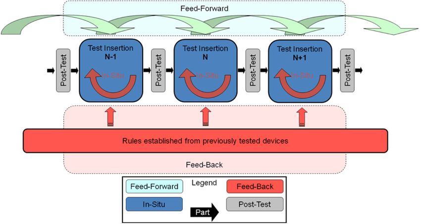
October, 2019                                                                                                                                                       Table of Contents

                                                                                      To download additional chapters, please visit
           Table of Contents                                                                        http://eps.ieee.org/hir

   CHAPTER 1: HETEROGENEOUS INTEGRATION ROADMAP: OVERVIEW .......................................................................... 1
   CHAPTER 2: HIGH PERFORMANCE COMPUTING AND DATA CENTERS ............................................................................. 1
   CHAPTER 3: THE INTERNET OF THINGS (IOT) .................................................................................................................. 1
   CHAPTER 4: MEDICAL, HEALTH & WEARABLES ............................................................................................................... 1
   CHAPTER 5: AUTOMOTIVE ............................................................................................................................................ 1
   CHAPTER 6: AEROSPACE AND DEFENSE ......................................................................................................................... 1
   CHAPTER 7: MOBILE ...................................................................................................................................................... 1
   CHAPTER 8: SINGLE CHIP AND MULTI CHIP INTEGRATION .............................................................................................. 1
   CHAPTER 9: INTEGRATED PHOTONICS ........................................................................................................................... 1
   CHAPTER 10: INTEGRATED POWER ELECTRONICS .......................................................................................................... 1
   CHAPTER 11: MEMS AND SENSOR INTEGRATION ........................................................................................................... 1
   CHAPTER 12: 5G COMMUNICATIONS............................................................................................................................. 1
   CHAPTER 13: CO DESIGN FOR HETEROGENEOUS INTEGRATION ..................................................................................... 1
   CHAPTER 14: MODELING AND SIMULATION .................................................................................................................. 1
   CHAPTER 15: MATERIALS AND EMERGING RESEARCH MATERIALS ................................................................................. 1
   CHAPTER 16: EMERGING RESEARCH DEVICES ................................................................................................................ 1
   CHAPTER 17: TEST TECHNOLOGY ................................................................................................................................... 1
     EXECUTIVE SUMMARY AND SCOPE ................................................................................................................................................ 1
     1. RF TEST ............................................................................................................................................................................... 4
     2. TEST OF PHOTONIC DEVICES .................................................................................................................................................... 7
     3. LOGIC DEVICE TESTING ......................................................................................................................................................... 20
     4. SPECIALTY DEVICE TESTING .................................................................................................................................................... 24
     5. MEMORY TEST .................................................................................................................................................................... 29
     6. ANALOG AND MIXED SIGNAL TEST .......................................................................................................................................... 31
     7. WAFER PROBE AND DEVICE HANDLING .................................................................................................................................... 35
     8. SYSTEM LEVEL TEST.............................................................................................................................................................. 44
     9. ADAPTIVE TEST ................................................................................................................................................................... 52
     10. DFT, CONCURRENT, AND SOC TESTING ................................................................................................................................. 66
     11. 2.5D & 3D DEVICE TESTING ............................................................................................................................................... 74
     12. BURN‐IN AND RELIABILITY TESTING ....................................................................................................................................... 78
     13. TEST AND YIELD LEARNING .................................................................................................................................................. 83
     14. COST OF TEST ................................................................................................................................................................... 85
   CHAPTER 18: SUPPLY CHAIN .......................................................................................................................................... 1
   CHAPTER 19: SECURITY ................................................................................................................................................. 1
   CHAPTER 20: THERMAL ................................................................................................................................................. 1
   CHAPTER 21: SIP AND MODULE SYSTEM INTEGRATION ................................................................................................. 1
   CHAPTER 22: INTERCONNECTS FOR 2D AND 3D ARCHITECTURES ................................................................................... 1
   CHAPTER 23: WAFER‐LEVEL PACKAGING (WLP) ............................................................................................................. 1

HIR Version 1.0 (eps.ieee.org/hir)                                                           Page ii                                    Heterogeneous Integration Roadmap
June, 2019                                                                                                Test Technology

Chapter 17: Test Technology
Executive Summary and Scope
    This bi-annual update to the heterogeneous integration testing roadmap contains our best estimates of key trends
influencing this industry over the next 15 years. This roadmap includes trends in semiconductor device technologies
and their impact on test, as well as roadmaps for key test enablers (Device Handlers, Test Interfaces, and Test
Methods). The resulting Cost of Test is also analyzed and discussed.
Key Implications per Device Technology
    RF Devices: The ramp of 5G devices is going to challenge the test industry in terms of frequency, port-count, and
lower noise margins. Additionally, production test methods for confronting beam-steering are of concern.
    High-Speed Digital Devices: Signal delivery through clean traces and a test interface (probe or socket) is becoming
a major concern as speeds move past 16 Gbps (today) to more than 60 Gbps during this roadmap timeline.
Deployment of multi-level technologies (PAM4) challenge noise margins and instrument designs. The large quantity
of high-speed digital interfaces per part is another challenge lacking an obvious solution.
    Photonic Devices: The large number of photonic standards together with an ever-increasing number of ports,
while geometries continue to shrink, is going to be a significant challenge for the industry to address in a cost-effective
manner.
    Logic Devices: Growing device complexity is having a big impact on the industry today. This trend is expected
to continue with pattern depths and structural test times doubling every three years over the roadmap period. Higher
complexity also drives up the device cooling requirements during test.
    Specialty Devices: The trend for tighter-pitch displays and cameras is resulting in a need for probing contacts of
finer pitch and smaller size. At the same time, higher volumes are driving the need for more test parallelism. The
large volume of inexpensive IoT sensor devices of various types will continue to challenge the industry.
    Memory Devices: NAND Flash device test times will continue to scale with higher densities. The introduction
of high-speed serial memory interfaces may change the test approach. Achieving Known-Good-Die (KGD) and
Known-Good-Stack (KGS) for memory devices destined for 2.5D and 3D integrations will continue to be of growing
importance.
    Analog/Mixed Signal Devices: Technology advances are expected to challenge mixed-signal devices in about
five years as speeds and resolutions increase while voltage swings continue to drop.
Key Implications per Device Handling and Contacting
    Device Handlers: Wafer probe and component test handling equipment face significant technical challenges in
each market segment. Common issues on both platforms include higher parallelism and more capable and flexible
thermal solutions, which result in increasing capital equipment and interface cost.
    Probes: The probe complexity roadmap continues to accelerate at challenging rates. Pad size and pitch are
expected to keep compressing with site counts increasing. With the manufacturing of super-high-speed serial and
5G devices, probe technology is being forced to provide cost-effective 40-80 GHz bandwidth solutions.
Key Implications for Test Methods
    System Level Testing (SLT): A resurgence in functional/SLT testing, especially at the module level, is a major
industry trend. The system-level boot-up test remains the critical acid test for most electronic systems. Efforts
continue to pinpoint the faults responsible for structural test failures. In the meantime, SLT deployments are expected
to rise.
    Adaptive Testing: This technology continues to ramp in many ways throughout the industry. Expansion will
be challenged by the explosion of data, the need for effective analysis, and response tools, which critically need a
universal data model/format to enable “Big Data” analysis independent of the source Further challenging this
methodology is multi-vendor integrations and data security concerns.
    Concurrent Testing: Expanded usage of concurrent test techniques is constrained by limitations in device access
(pins) as well as a lack in standardized tools and methods. A breakthrough for this technology will come when
efficient and standard test interfaces are implemented for analog and RF testing. Analog scan is one technology
starting to show progress.

HIR version 1.0 (eps.ieee.org/hir)             Chapter 17, Page 1                     Heterogeneous Integration Roadmap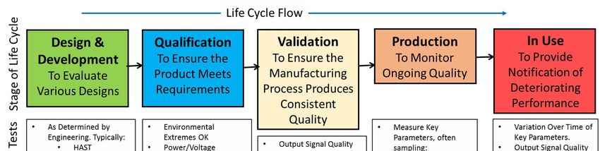
June, 2019                                                                                              Test Technology
    2.5D/3D Testing: Known-Good-Die (KGD) are very important today and will become even more important in
the future (larger parts with more gates, more devices per assembly). Achieving KGD will push test content earlier
in the manufacturing flow, challenging wafer- and/or die-level testing. Testing the multi-chip assembly is expected
to be done by traditional approaches including boundary-scan and system-level testing.
    Reliability Testing: Increased quality and reliability needs of the automotive and mobility integrated circuit
markets are driving additional test and burn-in requirements, including system-level test. Packaging innovation,
including the need for KGD, drives additional test fixturing and testing challenges, as does multi-die packaging.
    Design-For-Testability (DFT): Ongoing use of pattern compression and the use of hierarchical design
techniques is continuing to have a positive impact on pattern depths and device test times. The quest for higher
compression ratios is proving to be a difficult one.
    Yield Learning: Improvements are needed in resolving cell-internal defects. Achieving this goal will generate
significant amounts of data requiring careful analysis. Automotive reliability requirements are driving a change of
mindset away from structural test coverage being adequate to functional, system level, and in-situ testing techniques
becoming the new focus.
Key Implications for Cost of Test
    The cost of consumable products in device testing is starting to have a dominant impact on the industry moving
forward. The result is many anecdotal comments that moving to a new transistor geometry node has cost more in
terms of consumable products (probes, sockets, interface boards) than the cost of the test instrumentation to do the
new level of testing. Compounding this problem is the requirement for ongoing maintenance of these components
as well as their limited lifetime.
    Another major trend having a significant impact on the cost of semiconductor testing is longer test times.
Increased device complexity drive up the pattern depths and test times at a rate significantly faster than the rate of
complexity increases (exponentially). We no longer talk about test times of a few seconds and often end up with
test times of a few minutes. Without a breakthrough in scan testing speeds, this trend is expected to continue for
monolithic devices during this roadmap period.
    Heterogeneous integration will allow the large devices to be split up into smaller chips with the test time impact
now being exponentially reduced. Additionally, multiple smaller devices can usually be tested concurrently for
additional savings of test costs.
    Many efforts are expected to try and reduce test costs moving forward including higher parallelism, reduced test
time overhead, reduced equipment and consumable costs, etc. Despite these efforts, increased complexity and
demands for higher performance testing will likely cause the cost of leading-edge test solutions to increase
significantly.
Detailed Discussion of the Trends
    Each of the topics highlighted above as key implications for test moving forward are explored in precise details in
the next sections.
Acknowledgments
    This update to the test roadmap is output from a team of more than 120 test experts hailing from more than 50
companies world-wide. The leadership team for this effort is shown below:

 Dave Armstrong:                Chairman, Test Technology Working Group, Heterogeneous Integration Roadmap

 2.5D/3D device test            Bill Eklow                         Photonic Test              Dick Otte
 Adaptive test                  Phil Nigh                          Probe Cards                Dave Armstrong (Acting)
 Analog and Mixed-signal        Don Blair                          Prober                     Yoichi Shimizu
 Concurrent Test                Kenichi Anzou                      Radio Frequency            Don Blair
 Cost of Test                   Ken Lanier                         Reliability Testing        Carl Buck
 DFT & SOC Device Testing       Kenichi Anzou                      Specialty Device Testing   Wendy Chen
 Handlers                       Masahito Kondo                     System Level Test          Harry Chen
 High Speed IO Testing          Yi Cai                             Test and Yield Learning    Anne Gattiker
 Logic device test              Marc Hutner                        Test Sockets               Rick Marshal
 Memory Test                    Dave Armstrong (Acting)

HIR version 1.0 (eps.ieee.org/hir)            Chapter 17, Page 2                       Heterogeneous Integration Roadmap
June, 2019                                                                                               Test Technology
   Test Technology Working Group Contributors:
Stacy Ajouri, Lionel Kimerling, Mike Alfano, Craig Kirkpatrick, Kenichi Anzou, Leo Kluger, Takenori Aoki, Masahito Kondo,
Jeff Arasmith, Hiroshi Kurosaki, Dave Armstrong, Greg Labonte, Keith Arnold, Ken Lanier, Roger Barth, Lenny Leon, Brady
Benware, Ira Leventhal, Keren Bergman, Clark Liu, Paul Berndt, John MacWilliams, Mark Berry, TM Mak, Anil Bhalla,
Yiorgos Makris, Don Blair, Adriano Mancosu, Shawn Blanton, Peter Maxwell, Daniel Bock, Fabio Morgana, Bill Bottoms,
Franco Motika, Carl Bowan, Nilanjan Mukerjee, Carl Buck, Chris Nigh, Ken Butler, Phil Nigh, Yi Cai, Peter O'Neill, John
Caldwell, Richard Otte, John Carulli, Sule Ozev, Krishnendu Chakrabarty, Gilles, Wendy Chen, Jayson Park, Harry Chen, Mike
Peng Li, Wu-Tung Cheng, Jan Peters Weem, Vivek Chickermane, Robert Pfahl, Tim Cleary, Robert Polster, Chris Coleman,
Chris Portelli, Zoe Conroy, Dieter Rate, Adam Cron, Jeff Rearick, Al Crouch, Graham Reed, Robert Daasch, Herb Reiter, Dirk
de Vries, Joseph Reynick, Rao Desineni, Jason Rivers, Makoto Eiki, Mike Rodgers, Bill Eklow, Jeff Roehr, Dan Evans, Pete
Rogan, Ira Feldman, Mark Roos, Shawn Fetterolf, Rajiv Roy, Derek Floyd, Sam Salloum, Bert Gab, Ben Sarpong, Michael
Garner, Philip Schofield, Anne Gattiker, Michael Schuldenfrei, Xinli Gu, Rene Segers, Richard Hanvey, John Shelley, Ian
Harrison, Yoichi Shimizu, Don Hartman, Mustafa Slamani, Kazumi Hatayama, Wesley Smith, Klaus-Dieter Hilliges, Stephen
Sunter, Andy Hsu, Aoki Takenori, Tom Hsu, Steve Tilden, Marc Hutner, Srikanth Venkataraman, Shuichi Ito, Li-C Wang, Erik
Jan Marinissen, Thomas Williams, Rene Jonker, Scottie Wyatt, Matthias Kamm, Tian Xia, Rohit Kapur, John Yi, Brion Keller,
ChuHui Yu

HIR version 1.0 (eps.ieee.org/hir)            Chapter 17, Page 3                      Heterogeneous Integration Roadmap
June, 2019                                                                                                              Test Technology
Section 1: RF Test
Key Test Trends
                                                    Table 1: RF Test Requirements
      Year of Production                                                          2018         2019        2020         2025        2030
      Leading Edge (Note 1)
      Mobile Devices (General Radio) (Note 13)
      Carrier Frequency (GHz)                                                     8            8           8            8           8
      Number of simultaneously active RF Ports per Die (Note 11)                  12           16          16           16          16
      Total number of RF Ports per Die (Note 11)                                  48           64          64           64          64
      Modulation RF SSB BW (MHz) (Note 2)                                         80           80          80           80          80
June, 2019 Test Technology
Short Term Trends (65 GHz (mechanical and cost challenge), Integrating 3rd party components
into the test-head or probe card for applications >60 GHz, and blind mate connector BW performance at
40-80 GHz.
In the 5G space, there are more carrier bands/aggregation and more BW(IF - 2 GHz). Power
management may become an issue both in terms of number of domains and cooling dissipation during
test.
Impedance standards and calibration methods for high frequency measurement at probe need to be
created.
HIR version 1.0 (eps.ieee.org/hir) Chapter 17, Page 5 Heterogeneous Integration Roadmap
June, 2019 Test Technology
The EMI environment of the test development setup may be substantially different than the environment
on the production test floor, creating yield and correlation issues.
Most SOC test requirements are still trending from RF-to-BB and vice-versa. RF-to-Digital or line-to-
line is limited but widely discussed.
The increase in performance and frequency in combination with the economics of test will put a strong
focus on novel design-for-test and alternative test techniques to be developed in the coming years.
OEM is conceptualizing RF BIST/loop-back test methodology, but functional and parametric tests still
dominate the market.
Medium-Term Trends (6-10 years out)
In the backhaul transceiver space, phase array antennas will have a larger number of RF ports. For example,
satellite apps in the 12-40 GHz range with MCMs combining front end integration: ASICs, ADC and DACs.
Other examples include backhaul: transceivers with 3 ports (RX, LO, TX) per band combined with multi-band for
a total of as many as 9-11 ports; and 5G with a minimum 4 ports (2X2 antenna) and maximum of 64 ports for an 8X8
antenna.
With this increase in ports and IP blocks, there will be an increase of power needs in terms of the number of
domains and wattage (heat).
Difficult Challenges in the Medium Term
Test for phase-array transceivers will require cooling mechanism(s) during test.
There will be a need to integrate temperature sensors into the handler, device (on die) and wafer probe.
The higher the power, the faster the rate of change of temperature.
There will be a requirement to integrate cooling into the handler and wafer chuck.
COT challenges will be exacerbated for these solutions for cooling and number of RF ports.
LONG Term Trends (10+ years out)
6G future possible improvements include:
Integrate terrestrial wireless with satellite systems.
Ultra-dense cell networks, millimeter waves for user access, enhanced optical-wireless interface.
Difficult Challenges in the Long Term
The definition of 6G needs to firm up for the challenges to be known.
Trends impacting the roadmap 2017-19
The model presented in this roadmap was generated in 2017 and there are areas that need to be looked into further
for the next update.
5G both in the base station and appliances have been gaining significant momentum and will need to be
integrated into the tables with more details about frequency bands, different modes, channel bandwidth,
EVM requirements and number of channels.
An additional 5G topic, but one that deserves its own space in the tables as well is the 5G antennae which
are required for beam forming. Here the entries would include the frequency bands, array sizes, looking at
phase shifts between the antenna elements in the array, and the number of RF ports required to test the
array along with the other elements, such as a transceiver(s)
Summary
The number of RF ports increases significantly in categories such as backhaul transceivers and multi-band 5G.
With the increase in ports also comes higher power consumption, leading to higher heat generation. The Mobility
market continues to have higher cost pressures than the Infrastructure/Automotive RADAR/Industrial. ATE needs
to follow these trends with more RF ports, more power options and ways to deal with heat generation, while
maintaining or even decreasing the ATE costs.
References
https://www.keysight.com/upload/cmc_upload/All/20170608-A3-BrianSu.pdf
https://www.eetindia.co.in/news/article/new-wi-fi-standard-extends-mu-mimo-to-8x8-arrays
https://www.linkedin.com/pulse/beyond-5g-roadmap-6g-stephen-patrick/
HIR version 1.0 (eps.ieee.org/hir) Chapter 17, Page 6 Heterogeneous Integration Roadmap
June, 2019                                                                                                Test Technology
Section 2: Test of Photonic Devices
Executive Summary
    This section addresses overall lifetime test issues resulting from the inclusion of photonic capabilities into devices
and products. The emphasis is on silicon wafers and die with photonic functionality, and assemblies and products
that include these devices. Systems in Package (SiP) assemblies and systems are addressed to the extent viable given
the diversity of test needs that are specific to applications. The test issues for wafers, die, SiPs and systems will be
addressed at the Design, Qualification, Validation, Production and In-Use stages of life cycles. Current and
anticipated optical parameters to be tested and their value or level are considered along with the test access issue at
each stage of the product life cycle.
    Telecommunications test equipment, components and methods were and are being adopted for optical testing of
products used for non-long-haul applications. The traditional methods are being extended and new methods
developed to address test needs for photonic wafers, photonic integrated circuits, System in Package (SiP) that utilize
optics, and complete systems. Utilizing these extended methods requires optical probing of both wafers and die
combined with electrical probing, resulting in a series of mechanical issues. The inclusion of optical probing,
especially single mode probing, requires gratings or other access points on wafers. For individual die, dual mode
(electrical and optical) probing is especially difficult due to the small size of die and difficulty of holding and locating
probes accurately. At the SiP level, the problems are easier because the device is larger, not as fragile, and is often
designed to facilitate dual-media probing. The wafer, die and SiP probe fixtures tend to be expensive due to the
complexity and accuracy required. System-level test access is usually easier because at that level, electrical interfaces
and optical connectors are included as part of the DUT.
    In addition to probe access, optical test methods to simultaneous characterize and compare multiple optical lanes
and/or ports at the same time are needed. One need is comparative simultaneous testing of multiple signals from
arrays of ribbon fibers, waveguides or chip sources or detectors for optical skew, jitter, etc. A related need is
simultaneously evaluating optical signals multiplexed on one fiber or waveguide. Applications with arrays of up to
256 ports (fibers, waveguides chips) or ~256 multiplexed wavelengths are forecast in the next 10 years.
    In addition to the standard telecom optical parameters (power, wavelength, attenuation, jitter, SNR, etc.), emerging
applications utilize virtually every parameter that light can have, potentially requiring the extension of test capability
in multiple dimensions such as polarization, phase noise, spatial modes, multiple fiber cores, etc. While these
emerging needs are potentially very broad, the near-term emerging needs seem most likely to be extensions of data
communications needs.
    Optical communication applications are likely to utilize 650 nm to 1700 nm wavelengths, multiplexed wavelength
spacing down of 25 GHz, detector efficiency of ~1Amp/Watt, receiver sensitivity as great as -45 dBm, power levels
of 1 watt or less, symbol rates of 100 Gbaud per lane, modulation schemes utilizing up to 10 bits per symbol,
polarization multiplexing, BERs of 10-12, etc. Over time these parameters will improve, so test capabilities will need
to stay ahead of them. Data rates as high as 500 Tbps per fiber are likely to emerge in the next 10 to 15 years.
    Design for test by including optical test access points, Built In Self Test (BIST), redundancy for self repair and
prognostics to report changes and deterioration during operation over the life cycle of optical products are desirable
and of value in an increasing number of applications. These should be considered for inclusion not only in designs
but in software design tools as well.
     This section on photonics test contains our best estimates of key trends influencing this industry over the next
 15 years. This roadmap includes trends in semiconductor device technologies and their impact on test, as well
 as roadmaps for key test enablers (Device Handlers, Test Interfaces, and Test Methods). The resulting Cost of
 Test is also analyzed and discussed.

HIR version 1.0 (eps.ieee.org/hir)             Chapter 17, Page 7                      Heterogeneous Integration Roadmap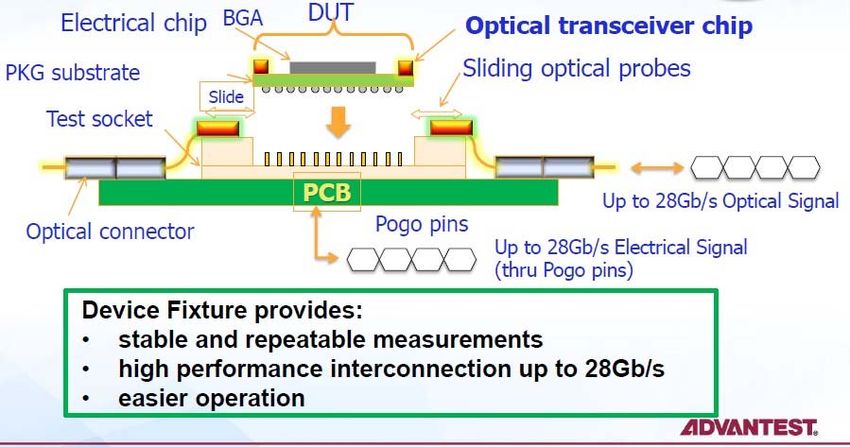
June, 2019 Test Technology
INTRODUCTION
This section focuses on unique attributes of testing optical
devices. No attempt has been made to duplicate required and Links vs Channels
typical electrical or mechanical testing. An optical link utilizes one wavelength
The chapter is open ended on optical applications testing traveling from one point to another in one fiber
with much of the material broadly applicable. It does, or waveguide. Information may be imposed on
however, concentrate primarily on testing data the beam utilizing any methods such as On-Off-
communications products. Keying, PAM XX, dual polarization or any
The section addresses photonic testing for: method that affects only that wavelength.
a. photonic integrated circuits (PICs) on wafer A Channel may consist of a single lane but
b. individual PIC die often, even usually, has multiple lanes. The
c. photonic System in Package (SiP) devices lanes may be on multiple parallel fibers or
d. system level optical functionality, such as a complete waveguides, or on the same fiber or waveguide
transceiver or Active Optical Cable (AOC). utilizing wavelength division multiplexing.
Another dimension addressed is testing needs over a Many datacom standards utilize multiple lanes
product life cycle: to achieve their data rates.
a. during development to prove functionality and Evaluating technical capability is most easily
de-bug devices done utilizing lanes because channels that
b. qualification testing combine many lanes make it difficult to
c. pre-production validation understand the underlying technology. System
d. in-process production testing to assure product quality designers, however, find the channel view more
and improve yield. useful as the technology details are not
important at their level.
SITUATION (INFRASTRUCTURE) ANALYSIS
Generic Photonic Device Testing
Figure 1 illustrates the general test requirement; the need for both electrical and optical test inputs, and then
analysis of the electrical and optical outputs from the device under test (DUT). In addition, environmental parameters,
such as temperature, humidity, vibration, etc. may be test inputs. Finally, in addition to the optical and electrical test
responses, physical factors such as temperature rise may be outputs that are monitored during testing.
Figure 1. Generic Photonic Product Test Environment
The electrical ports are electrical contacts, or arrays of contacts, for power, control, monitoring of functionality
and of course data inputs and/or outputs.
Optical input ports may provide optical beam/s to be modulated or data streams, often in arrays, to be analyzed.
The optical “connections” may be a butt coupling, an air gap with a beam bridging into the device or an evanescent
coupling resulting from proximity of waveguides. Making these test connections, especially the optical connections,
is frequently a major project.
The photonic input and output signals may have multiple parameters. Specifically, optical signals may have:
Intensity
Polarization
HIR version 1.0 (eps.ieee.org/hir) Chapter 17, Page 8 Heterogeneous Integration RoadmapJune, 2019 Test Technology
Direction
Mode profile
Wavelength
Variation over time:
modulation (fast)
drift (slow)
Skew between beams
Signal-to-Noise Ratio (SNR, RIN, Crosstalk)
Bit error rate (BER)
One or more of these parameters must be imposed on a suitable optical beam or beams and injected into devices
on the optical ports to provide a drive signal. The device under test will perform a function determined not only by
the input optical signals, but by the electrical inputs as well. The resulting electrical and optical signals are on the
corresponding output ports.
Environmental inputs may include all of the usual variables: temperature, humidity, temperature cycling, Highly
Accelerated Stress Test (HAST), vibration, shock, etc.
Physical outputs include temperature rise, mechanical changes such as delamination, cracking, swelling, wire
breaks or optical chain interruptions, etc.
Photonic test requirements vary by the test level (wafer, die, photonic SiP, system) and test need (access, sources,
detectors, functions). Table 1, Photonic Test Requirements, gives a generic view of the testing needs for items
containing photonic elements at the various levels.
A similar table can be developed for specific applications to provide some insight into the related requirements
for each application.
Several types of product testing of devices, including those with photonic capability, are usually required:
Test during development to ensure the design “works”.
Qualification testing, typically done before a product is committed to wide use.
In-process testing to monitor manufacturing process quality.
Final testing before each individual product is shipped to a customer.
Every application, including photonic products, has a specific set of these tests that is applicable to that product.
Data communication is an application of immediate interest, one of the most important at the moment, and an
application about which much is known; hence we will concentrate on it.
HIR version 1.0 (eps.ieee.org/hir) Chapter 17, Page 9 Heterogeneous Integration RoadmapJune, 2019 Test Technology
Table 1. Photonic Test Requirements
Test Need
Test Level Optical Access Sources Detectors Functions
Wafer 45o mirrors, vertical External sources External photo-detectors, Wide variety of device
grating couplers, cleaved injected via fiber or potentially in arrays; characterization and functional
fiber, tapered fiber, free-space access Imaging sensors (eg. tests; media loss/cm, insertion
lensed fiber, focused CCD/CMOS FPAs); loss, modulation depth/
free-space beam, Integrated sources Optics to collect and/or bandwidth, polarization control,
evanescent coupling image light to be wafer uniformity, detector
detected. sensitivity/responsivity,
temperature sensitivity, die-to-
Integrated photodetectors die variation, skew between
outputs
Chip Wafer options Wafer options Wafer options Wafer options plus edge
plus edge coupling to coupling impacts on loss,
embedded or surface spectral bandwidth and
waveguides. polarization
Photonic SiP Butt coupling or External or on-chip External detector or Wafer and chip options, plus
expanded beam laser source to detectors, potentially in characterize package
connector, evanescent simulate application an array, gathering light connections, and application
coupling, fiber splice, related requirements. from an edge emitting specific tests such as eye
ribbon fiber splice waveguide or vertical diagrams, BER, environmental
emitting 45o mirror, or sensitivity
vertical emitting grating
System Conventional optical External or internal As needed to measure Intensity, skew between lanes,
connector, fiber splice laser source or sources and evaluate system polarization, eye diagram, SNR
to simulate inputs. outputs.
In Use, Over Limited, if any. Both self and remotely Primarily wireless or Monitor & report performance
Lifetime Primarily wireless or initiated data reporting electronic changes. Initiate self-repair.
electronic
Data Communications Device Testing
Some specific points and issues important in testing data communications photonic products, especially
transceivers, are these:
i) Test time is being increased by IEEE Standards that “stretch” the required reach. That reduces SNR and
rapidly raises the BER. Thus, “wisely” managing the required reach reduces test cost.
ii) For some data communication applications, a simple, “worst case” Eye Diagram Test is sufficient. This point
illustrates that choosing the right criteria that properly balances the test need and potential faults can reduce
test cost.
iii) Some Optical Components, especially lasers, are nonlinear, so testing is harder to do and more demanding,
but also more important.
The need for specific, high-tolerance physical location of optical components during testing makes changing
optical test configurations difficult and time consuming. Gradually reducing input signal strength and measuring the
decrease in performance can sometimes provide a way to determine margin and robustness of Optical Systems. This
approach, of course, is widely used as one criteria/methodology for electronic products.
Developing new test software, fixtures, sources, detectors, etc. often takes a long time and depends on the materials
and devices to be tested. Optical engineers are innovative and continually developing new design and test methods.
Fortunately, low volume test capability is improving to support researchers. (These capabilities may eventually
impact high volume needs.)
HIR version 1.0 (eps.ieee.org/hir) Chapter 17, Page 10 Heterogeneous Integration RoadmapJune, 2019 Test Technology
Test Equipment
Optical device test equipment is available from multiple suppliers. Historically, the telecommunications industry
was the major consumer, but in recent years the use of optical communications for short distances, such as LANS,
FTTX, and AOC and in Data Centers, as well as a variety of sensors, has broadened the demand. Much of the demand
emerging for these new optical applications is filled by utilizing equipment developed for and derived from that used
by the Telecom sector. As these applications grow in importance, specialized equipment is emerging and becoming
available.
Test Processes
Bit Error Rate (BER) Testing is the most time-consuming and therefore more expensive than other testing.
Eye diagram evaluation is of great value and one of the most common test methods for data communications
devices.
A related test methodology is “constellation measurement” used for characterizing complex modulation schemes
such as QAMXX. Several versions of this method are in use depending on the modulation scheme to be evaluated.
Test Access, Fixtures and Methods
PIC Layout for Test:
Layout photonic chips and substrates to facilitate testing and packaging by enabling optical access for
simultaneous multi-channel optical probes as well as DC, RF and microwave electrical probes.
Route all optical I/O to the same device edge, organized in a standard linear array; e. g., 127 um or 250
um pitch. All optical ports can be accessed simultaneously by alignment of a single fiber array probe.
DC and RF pads should similarly be routed to a single, although different, device edge to allow
simultaneous probing with multi-conductor probe cards. Ideally only four independent probe heads
need to be aligned, to the North, South, East and West edges of the device. Anticipate interference of
probe structure mounts when designing compact devices.
Include on-wafer/chip test structures for calibrating probes.
Include on-wafer/chip test devices for characterizing individual components, in isolation from a
complex, integrated system.
Incorporate Built In Self Test (BIST) whenever possible.
Enable debug of faulty circuits by designing test points (grating couplers or photodiodes) to tap off
signals. Might make use of the CLIPP (Contactless Integrated Photonic Probe).
Wafer DUT Interface:
Optical probes must interface by surface grating couplers which impose limits of narrower spectral
bandwidth and polarization dependency. Alternative vertical coupling technologies could include
etched turn mirrors. Possible for grating couplers to be diced off during singulation, so the final chip is
edge-coupled.
Optical probes can be: single-channel, multi-channel, SMF, PMF, flat facet (cleave, UPC), APC.
facet, lensed, tapered.
Optical probe alignment should ideally have 6 degrees of freedom, with 0.1 micron translational
precision, and 0.3 arcminute rotational precision.1
Test on an opto-electronic probe station (manual or automated) with a temperature-controlled wafer
chuck. A commercially available system from PI is shown in figure 2. A video of it in action is at the
following link: https://www.youtube.com/embed/_TG3lUu-k0k?rel=0
1
The 0.3 arc minute requirement is pointing accuracy required for free space beam such as encountered in Lidar and other
free space applications. The requirement in most datacom applications is significantly less, such as 1° which is required for
simultaneous alignment of multiple fiber probes in a linear array.
HIR version 1.0 (eps.ieee.org/hir) Chapter 17, Page 11 Heterogeneous Integration RoadmapJune, 2019 Test Technology
Figure 2. A PI Wafer Probe Station for photonic integrated circuits.
Chip DUT Interface:
Figure 3. PI Probe Station Concept for Individual PICs.
Probing individual chips as suggested in Figure 3 and earlier in Table 1 is viable under some conditions but is
generally to be avoided, with wafer-level testing preferred. Individual PIC testing has not only the usual optical and
electrical probe interface issues but the added issues of handling and aligning an individual die. Handling is
particularly difficult for thin die, meaning 100 microns, that are commonly used.
Whenever necessary, however, test capability for chips is available commercially, even for PICs.
Packaged device DUT interface:
Testing during development on a lab bench: Temperature control is possible through the use of a thermal-stream
forced air system. Connections are made through standard connectors (optical and electrical). No probes are
required.
One version of a test fixture suitable for products with both electrical and photonic inputs and outputs is illustrated
below in Figure 4. This is a highly custom fixture designed specifically for the device to be tested. The configuration
is viable because the device configuration, meaning locations of optical and electrical access points, is chosen with
the fixture needed to make connection in mind. The electrical connections through pogo pins is well known but does
put stress on the DUT, causing it to deform to varying degrees depending on dimensions, temperature, etc. These
physical changes make interfacing the optical ports more complex as they must move not only laterally, but somehow
be keyed to align in the other 2 dimensions as well as 2 angular dimensions. This might be accomplished with pins,
for example, commonly used with the US Conec optical connectors. That, of course, will make the fixture more
complex than suggested by Figure 4.
HIR version 1.0 (eps.ieee.org/hir) Chapter 17, Page 12 Heterogeneous Integration RoadmapJune, 2019 Test Technology
Figure 4. A Test Fixture with both Optical and Electrical probes.
Design Tools and Design for Test
Design tools for PICs are starting to emerge. Including consideration of test will contribute to minimizing the cost
and difficulty of optical element test and raise the reliability of the end devices. PICs with many optical elements
and/or optical functions may benefit from on/in-chip optical ports to inject optical test signals or ports to probe optical
signals. Optical IO test ports can be included as gratings or splitters that allow injection or tapping of signals. These
could be in addition to vertical and horizontal ports that communicate on-to and off-of chip for regular IO functions.
Test Standards
The most complete set of optical data communications standards are published by Telcordia. The standards for
Optical Fiber and Equipment can be found at: http://telecom-info.telcordia.com/site-cgi/ido/docs2.pl
?ID=187033671&page=docs_doc_center. These standards related to telecommunications, of course, and are
applicable to system-level test requirements and to high reliability systems. Less demanding standards are needed
for primarily commercial and industrial applications.
Standard Physical Platforms, meaning photonic wafer fabrication methods and a related process design kit (PDK)
that Applications can be built on, have not emerged. Fortunately developing and making available such a platform
is one of the objectives of AIM-IP. The photonic industry will be able to support a minimal number of innovations,
so the sooner standardized packaging emerges, the better.
The PDK that AIM-IP is offering will limit innovation, so it is important that AIM-IP choose its PDK wisely and
that the PDK evolves in response to user needs and demands. The AIM MPW capability will be important to
Universities and Innovation.
The kinds of testing required vary over the life cycle of a product. Figure 5 below lists typical optical device test
activities and requirements over the life of a device from conception through the in-use and end of life phases.
HIR version 1.0 (eps.ieee.org/hir) Chapter 17, Page 13 Heterogeneous Integration RoadmapJune, 2019 Test Technology
Figure 5. Test Needs over An Optical Product Life Cycle
Environmental Technology
Optical Test has minimal environmental issues other than a few safety requirements associated with laser intensity
or UV hazards.
Separately, the environment in which optical devices must perform, and the related proof of performance test
evaluations they must be subjected to, have a wide range. A very demanding requirement is the classic Telecordia
telecommunications standards to ensure 40-year life. These are still required for some products, such as sub-sea
amplifiers. At the other extreme are consumer disposable that have minimal requirements. Between these extremes
are a variety of environments in which development and qualification tests must ensure performance.
Generic Test, Inspection and Measurement (TIM)
Types of measurements, O/O, O/E, E/O, E/E: Wafer characterization:
Wafer mapping: inking for good die identification, yield calculations, process improvement.
Wafer metrology: layer thicknesses, surface roughness, haze, feature definition, step heights, sheet
resistance, doping profiles, mature industry.
Device characterization:
Waveguides: Modal structure, group velocity, dispersion, loss, power handling, polarization dependence,
Rayleigh scatter, nonlinear limits (i.e., characterize second and third order susceptibility coefficients, SHG,
SFG, DFG, Raman, Brillouin, SPM, XPM, FWM)
Photodiode: Responsivity vs wavelength, polarization dependent loss, dark IV Curves (extract dark current,
diode ideality factor, series resistance), bandwidth vs bias, linearity, power handling/compression, over-
temperature sensitivity, input capacitance and resistance
Laser diode: LIV curves (extract threshold, slope efficiency, power saturation), RIN, SMSR, center wavelength,
linewidth, frequency noise, ASE, tuning coefficients, tuning range/rate, direct modulation bandwidth, over-
temperature sensitivity, tolerance to optical feedback
SOAs: spectral gain, efficiency, bandwidth, saturation power, noise figure, amplified spontaneous emission,
input power dynamic range
Modulators: extinction ratio vs input signal swing, input capacitance and resistance, electrical to optical
bandwidth, spectral bandwidth, insertion loss, polarization dependent loss, resonance frequency and free
spectral range and reflected power if applicable, dependence of extinction and optical bandwidth on biasing
point
HIR version 1.0 (eps.ieee.org/hir) Chapter 17, Page 14 Heterogeneous Integration RoadmapJune, 2019 Test Technology
Splitters/Combiners: split ratio, insertion loss, wavelength dependence, polarization dependence, reflected
power
Filters: band pass/band reject, attenuation/loss, center wavelength, bandwidth, ‘Q’ and free spectral range and
reflected power if applicable, dependence of extinction and optical bandwidth on biasing point, polarization
dependence, tunability: speed, efficiency, performance impact
Attenuators: center wavelength, bandwidth, attenuation, polarization dependence, reflected power vs
wavelength and polarization
Polarizers: degree of rejection, insertion loss, reflected power vs wavelength and polarization
Fiber Couplers: optical bandwidth, insertion loss, polarization dependent loss, reflected power
Switches: crosstalk, extinction ratio vs input signal swing, input capacitance and resistance, electrical to optical
bandwidth, optical bandwidth, insertion loss, polarization dependent loss, resonance frequency and free
spectral range and reflected power if applicable
Optical Connector Characterization:
The incorporation of optical connectors to build systems is increasingly important as a means to eliminate fiber
pigtails to reduce handling and the size of systems. Connectors, however, introduce another variable that must be
controlled and measured/tested.
Specific component and system characterizations to be performed related to connectors include:
Connector loss.
Wavelength dependence of connector loss.
Connector return loss.
Connector polarization-dependent loss.
Connector re-mating loss variation.
Dust contamination induced connector loss (test TBD).
Telcordia GR-1435 Uncontrolled Environment Thermal Aging, Humidity Aging, Thermal Cycling, and
Humidity/Condensation Cycling testing.
Signal Bit Error Rate vs. connector number and loss (25 Gbps/channel).
Estimated system implementation cost.
Functional tests
The most demanding test requirements are found in single mode applications so those are addressed below.
Multimode signal testing is usually less demanding.
The Telecom Industry utilizes single mode technology over hundreds of kilometers and has led the development
of optical test equipment and capability. Much of that equipment can be adopted for use with products being
developed for the emerging needs for shorter distances.
Data communications test needs differ from Telecom in that they tend to utilize more parallel signal transmission
through parallel media, either ribbon fiber or waveguide arrays, transmit light shorter distances are impaired by modal
dispersion and sometimes utilize more complex modulation schemes.
The general optical signal technical properties and test parameters follow in Table 2 below.
HIR version 1.0 (eps.ieee.org/hir) Chapter 17, Page 15 Heterogeneous Integration RoadmapJune, 2019 Test Technology
Table 2. Optical Test Parameters, Values, Media and Ranges
Parameter Range Comment
Optical Signal Characteristics
Wavelength 750 to 1,650 nm These are the primary wavelengths used for optical communications.
Longer, and sometimes shorter, wavelengths are used in sensors and
analytic applications.
Optical powerJune, 2019 Test Technology
Education and Training
Test is essentially a manufacturing activity and thus requires education and training in a series of disciplines and
skills. Tables 3 and 4 below provide some guidance on these needs.
Table 3. Academic Education Requirements
Knowledge Required Content
AC/and DC electricity Voltage, current, frequency, power, electronics, transformers, capacitors, inductors,
& electronics transistors, ions, conductors, semiconductors, non-conductors electrical to optical and
optical to electronic conversion.
Basics of Optics Ray tracing, lenses, mirrors, prisms, wavelength, phase, polarization, intensity, beam
divergence, beam focus, optical modes, E and H fields as related to the Poynting
Vector, light in fibers, both single and multimode, etc.
Characteristics of Signals Power, transmitting information, signal to noise ratio, modulation methods including
OOK, orthogonal signals, multiplexing, demultiplexing, Shannon Limit, etc.
Basics of Statistics Gathering data, maintaining integrity, managing data bases, standard deviation, mean,
median, Parato charts, statistical process control, control limits, Cp, Cpk, etc.
Measurements Basics of mechanical, electrical, optical metrology. Repeatability, gage studies, etc.
Financial basics Basic business financial concepts; revenue, costs, elements of cost, product cost
elements, overhead, cash, AR, AP, depreciation, equity, etc. “The $ in must be greater
than the $ out”. “We make investments in order to make more money back utilizing
the result of the investment,” etc.
Table 4. Training Requirements
Skill Required Areas of Training*
Personal Behavior Show up on time. Be prepared to perform your job. (Be present mentally and not
preoccupied with a non-job related issue, rested, healthy, properly dressed, etc.)
Safety Rules, behavior, precautions, etc., related to safety for machinery,
chemicals, slips and falls, people related, spills, MSDSs.
Quality Follow the rules. Ensure procedures are followed. Go beyond the formal requirements and
propose improvements. Follow the Japanese “5S” rules. Follow “Deming’s 14 Rules For
Management”. Use statistics to improve yield and minimize variation.
Cost Why cost is important, sources of cost, minimizing cost, proposing cost
reductions, minimizing waste, maximizing reuse and recycling.
Equipment operation Safe operation, instrument setup, calibration, standard operations, maintaining records,
impact of each process on cost, use of the operating manual, machine maintenance.
Metrology Use of calipers, electronic and optical measurement methods, storage of data and analysis,
ensuring accuracy.
Interpreting Read what it says, ask question, make sure you understand, do not
Instructions “assume”, eliminate and resolve ambiguities,
Completing Jobs On Ensure you understand what is required; ensure all of the instructions, materials equipment
Time and other resources are available. Start as soon as possible. Look for potential barriers
ahead and ensue they are eliminated. Be prepared to revise your approach. Ask for help.
When you error, admit you made a mistake, learn from it, ensure you do not make it again.
Do not hide your errors.
*While training is often highly specific to each job, basics apply to all jobs.
HIR version 1.0 (eps.ieee.org/hir) Chapter 17, Page 17 Heterogeneous Integration RoadmapJune, 2019 Test Technology
Figure 6: Test, Key Attributes
TECHNOLOGY NEEDS
Prioritized Research Needs (< 5 year results)
Processing ever faster (100Gbps+) data streams.
Test time is often determined and limited by memory IO data rates, so increasing these will remove a
barrier to lower cost.
Developing test equipment with more capability than the devices to be tested is a continually moving
target!
Flexible Test Platform, compatible with the test needs of different applications.
Ability to test photonic properties of wafers during fab to ensure wafers are good.
Prioritized Development & Implementation Needs (> 5 year result)
Eventually, the ability to support 500 Tbps/fiber data transfer rates is going to be needed. An important issue is
the nature of the data stream; how much parallelism, what modulation format, etc.
Gaps & Showstoppers
Table 5. Gaps and Showstoppers
The 50 GHz barrier resulting from conventional CMOS capability forcing parallel solutions
rather than higher baud rates.
Low speed of suitable assembly, test and other process equipment resulting in high costs.
Inability to overcome the cost driving, rate limiting step/bottle neck of manufacturing/testing such as the
number of assembly steps or length of time to perform test, especially BER testing. “Time is money”
Limits resulting from adapting existing equipment, materials and methods to optical test
because more specific equipment is not available because the demand is not sufficient to
incentivize equipment manufacturers to make it available.
Designing for Manufacturing and test:
Maximizing output to reduce cost
Studying designs to trade off accuracy and speed
Inability to utilize materials or processes due to environmental related constraints (RoHS,
REACH, WEEE, etc.)
HIR version 1.0 (eps.ieee.org/hir) Chapter 17, Page 18 Heterogeneous Integration RoadmapJune, 2019 Test Technology
RECOMMENDATIONS ON POTENTIAL ALTERNATIVE TECHNOLOGIES
Table 6. Recommendations for Potential Alternative Technologies
Utilize laser processing to make optical waveguides in-situ to effective optical connections and optical
structures.
Utilization of plasmons to minimize size and maximize functionality
Table 7. Types of Instruments Used for Optical Device Testing
Optical Vector Network Analyzer (OVNA) Optical Wavemeter
Lightwave Communication Analyzer (LCA) RIN measurement system
Electrical Vector Network Analyzer (VNA) Frequency noise test system
Optical Backscatter Reflectometer (OBR) Polarization controllers/analyzers
Swept tunable laser source (TLS) Optical attenuators and amplifiers
Fixed laser sources Real-time Oscilloscope
Power meters – optical and RF/microwave Digital Communication Analyzer (DCA)
Fast photo-receivers Bit-Error Rate Tester (BERT)
Optical Modulation Analyzer (OMA) IR camera to look at mode profiles, and scattered light
Optical Modulation Generator Ellipsometer
Optical Spectrum Analyzer (OSA) White light surface profilometer
Electrical Vector Spectrum/Signal Analyzer Optical microscope; SEM
Electrical Vector Signal Generator AFM
HIR version 1.0 (eps.ieee.org/hir) Chapter 17, Page 19 Heterogeneous Integration RoadmapJune, 2019 Test Technology
Section 3: Logic Device Testing
The focus of this section is the testing of CMOS digital logic portions of highly complex digital logic devices such
as microprocessors, and more generally the testing of logic cores that could stand-alone or be integrated into more
complex devices. Of primary concern will be the trends of key logic test attributes assuming the continuation of
fundamental roadmap trends. The “high volume microprocessor” and the “consumer SoC” devices are chosen as the
primary reference because the most trend data are available for them. Specific test requirements for embedded
memory (such as cache), I/O, mixed-signal, or RF are addressed in their respective chapters and must also be
comprehended when considering complex logic devices that contain these technologies.
Key Logic Device Testing Trends
The trends in Table 1 are extracted from other parts of the roadmap and are reproduced here to form the foundation
of key assumptions used to forecast future logic testing requirements. The first two line-items in the table show the
trends of functions per chip (number of transistors) and chip size at production. Chip size in terms of area is held
relatively constant aside from incremental yearly reductions within a process generation. The next line item reflects
a trend toward multiple core designs to address, in part, what has become the primary microprocessor scaling
constraint – the diminishing returns of clock frequency increases. There is a trend to greatly increase the number of
cores within each process generation and these will include multiple cores of a particular instruction set, but also
include other types of cores, such as graphics units (GPUs), Specialized I/O units (e.g. USB) and various other cores
not necessarily specific to a microprocessor.
The internal scan data rate of a device is the rate at which ATPG data can be shifted across the scan latches between
test sequences. These are commonly known as load/unload sequences. In the ITRS roadmap this was assumed to be
increasing by a percentage increase per year (15%). There are several reasons why this trend has a fundamental limit.
The toggle rate for scan, which translates to power utilization of the device under test, is much higher than for
functional operation of the device. The device would consume significantly higher power during test, which
translates to power degradation of supply levels, higher temperature of operation and a shift in operating point of the
logic elements under test. As devices move to finer-pitch geometries, the voltage levels required are also reducing,
which further impacts the effects mentioned. In addition to power demands, the timing closure of scan paths is also
more difficult at higher frequencies, resulting in a significant amount of work to ensure high speed operation. As a
result, the HIR roadmap projects that as devices reach frequencies of 125-150MHz for internal scan rate, the rates
will no longer increase compared to historical rates.
The effective scan compression rate will continue to increase, but the increase is accounted for in a different way.
The Logic Assumption sheet reflects the effectiveness of compression of a single IP block or subsystem.
Effectiveness of compression at this level of the design is slowing. Several years ago, the concept of hierarchal scan
was introduced by the EDA community. This is accounted for in the Logic Test Data Volume requirement, Table 2,
and realized with the number of identical IP blocks, where the same patterns could be applied at the same time.
In recent years, the fault models used for logic test have also improved. The shift was from a fault model based
on a Boolean equation to one based on transistor configuration. This has been accounted for in the models by starting
the projections from a transistor count rather than equivalent gates/functions. Presently the increased pattern count
has been counterbalanced by improvements in compression and scan-rate increase. As new fault models are
introduced to reach enhanced quality goals, the data volume may increase beyond what is projected in our model.
This will be addressed in a future revision of the HIR roadmap.
HIR version 1.0 (eps.ieee.org/hir) Chapter 17, Page 20 Heterogeneous Integration RoadmapYou can also read


