Lawrence Berkeley National Laboratory - Recent Work
←
→
Page content transcription
If your browser does not render page correctly, please read the page content below
Lawrence Berkeley National Laboratory
Recent Work

Title
Roadmap on Integrated Quantum Photonics

Permalink
https://escholarship.org/uc/item/04d4769v

Authors
Moody, Galan
Sorger, Volker J
Juodawlkis, Paul W
et al.

Publication Date
2021-02-18

Peer reviewed

 eScholarship.org Powered by the California Digital Library
 University of California
Journal of Physics: Photonics (2021) ###### Roadmap

Roadmap on Integrated Quantum Photonics
Galan Moody1, Volker J. Sorger2, Paul W. Juodawlkis3, William Loh3, Cheryl Sorace-Agaskar3, Marcelo
Davanco4, Lin Chang1, John E. Bowers1, Niels Quack5, Christophe Galland5, Igor Aharonovich6, M. A.
Wolff,7 C. Schuck7, Neil Sinclair8, Marko Lončar8, Tin Komljenovic9, David Weld1, Shayan Mookherjea10,
Sonia Buckley4, Marina Radulaski11, Stephan Reitzenstein12, Benjamin Pingault8,13, Bartholomeus
Machielse8, Debsuvra Mukhopadhyay14, Alexey Akimov14,15,16, Aleksei Zheltikov15,16,17, Girish S.
Agarwal14, Kartik Srinivasan4, Juanjuan Lu18, Hong X. Tang18, Wentao Jiang19, Timothy P. McKenna19,
Amir H. Safavi-Naeini19, Stephan Steinhauer20, Ali W. Elshaari20, Val Zwiller20, Paul S. Davids21, Nicholas
Martinez21, Michael Gehl21, John Chiaverini3, Karan K. Mehta22, Jacquiline Romero23,24, Navin B.
Lingaraju25, Andrew M. Weiner25, Daniel Peace26, Robert Cernansky26, Mirko Lobino26, Eleni
Diamanti27,28, Luis Trigo Vidarte27,28 and Ryan M. Camacho29

1 - University of California, Santa Barbara, USA
2 – George Washington University, USA
3 –MIT Lincoln Laboratory, USA
4 - National Institute of Standards and Technology, USA
5 - École Polytechnique Dédérale de Lausanne, Switzerland
6 – University of Technology Sydney, Australia
7 - University of Münster, Germany
8 - Harvard University, USA
9 - Nexus Photonics, Goleta, USA
10 – University of California, San Diego, USA
11 - University of California, Davis, USA
12 - Technische Universität Berlin, Germany
13 - QuTech, Delft University of Technology, Delft, The Netherlands
14 - Texas A&M University, USA
15 - PN Lebedev Physical Institute, Moscow, Russia
16 - Russian Quantum Center, Moscow Region, Russia
17 - M.V. Lomonosov Moscow State University, Moscow, Russia
18 – Yale University, USA
19 – Stanford University, USA
20 - KTH Royal Institute of Technology, Sweden
21 - Sandia National Labs, USA
22 – ETH Zurich, Switzerland
23 - Australian Research Council Centre of Excellence for Engineered Quantum Systems (EQUS), Australia
24 - University of Queensland, Australia
25 - Purdue University, USA
26 - Griffith University, Australia
27 - Centre National de la Recherche Scientifique, France
28 – Sorbonne University, France
29 - Brigham Young University, USA
Journal of Physics: Photonics (2021) ###### Roadmap

Contents
 1 - Introduction ................................................................................................................................... 3
PHOTONIC CIRCUIT INTEGRATED PLATFORMS ....................................................................................... 6
 2 - Heterogeneous Integrated Photonics for Quantum Information Science and Engineering ......... 6
 3 - Heterogeneous Integration Methods with III-V Quantum Dots .................................................. 11
 4 - AlGaAsOI Integrated Quantum Photonics ................................................................................... 14
 5 – Integrated Quantum Photonics in Diamond ............................................................................... 18
 6 – Integrated Quantum and Nonlinear Photonics with Tantalum Pentoxide ................................. 21
 7 – Quantum Photonics with Thin-Film Lithium Niobate ................................................................. 25
QUANTUM AND CLASSICAL LIGHT SOURCES AND QUBITS................................................................... 30
 8 - Heterogeneous Integration of High-Performance Lasers for Quantum Applications ................. 30
 9 - Chip-scale Entangled-Photon Sources ......................................................................................... 34
 10 - Sources and Qubits - Emissive Centers in Silicon....................................................................... 37
 11 - Integrated Photonics with Silicon Carbide Color Centers .......................................................... 40
 12 - O-band and C-band Single Quantum Emitters........................................................................... 43
 13 - Diamond Integrated Quantum Photonics.................................................................................. 46
 14 - Quantum Optics in Integrated Waveguides and Photonic Crystal Fibres ................................. 51
QUANTUM FREQUENCY CONVERSION ................................................................................................. 55
 15 - Quantum frequency conversion using integrated nanophotonics ............................................ 55
 16 - Single-Photon Nonlinearity in Integrated Quantum Photonics ................................................. 59
 17 - Quantum Transducers ............................................................................................................... 62
INTEGRATED DETECTORS ...................................................................................................................... 67
 18 - Waveguide-Integrated Superconducting Single-Photon Detectors .......................................... 67
 19 – Integrated Waveguide-Coupled Single Photon Detection Near Room Temperature............... 71
APPLICATIONS ....................................................................................................................................... 75
 20 – Photonics for Trapped-Ion Quantum Systems .......................................................................... 75
 21 – Photonic Qudits on Chip ........................................................................................................... 79
 22 – Frequency Bin Quantum Photonics .......................................................................................... 84
 23 – Continuous Variables Computing with Lithium Niobate Photonics .......................................... 88
 24 – Quantum Cryptography ............................................................................................................ 92
 25 – Machine Learning for Photonics ............................................................................................... 96
Journal of Physics: Photonics (2021) ###### Roadmap 1 - Introduction Galan Moody1 and Volker J. Sorger2 1 University of California Santa Barbara, Santa Barbara, CA, USA 2 George Washington University, Washington D.C., USA The Quantum Tyranny of Numbers In the 1960s, computer engineers had to address the tyranny of numbers problem in which improvements in computing and its applications required integrating an increasing number of electronic components and wires. From the first room-size computers powered by vacuum tubes to the billions of transistors fabricated on a single microprocessor chip today, transformational advances in integration have led to remarkable processing performance and new unforeseen applications in computing. Today, quantum scientists and engineers are facing similar integration challenges with solid-state, atomic, and photonic quantum systems for computing, communications, and sensing. Research labs packed with benchtop components, such as tunable and narrow-linewidth lasers, tables filled with optics, and racks of control hardware, are needed to prepare, manipulate, and read out quantum states from a modest number of quantum bits (qubits). Analogous to electronic circuit design and fabrication nearly five decades ago, scaling quantum systems (i.e. to thousands or millions of components and quantum elements) with the required functionality, high performance, and stability will only be realized through novel design architectures and fabrication techniques that enable the chip-scale integration of electronic and quantum photonic integrated circuits (QPIC). In the last decade, remarkable advances along this direction have enabled the functionality of benchtop experiments to be scaled down to prototype chips with improvements in system-wide efficiency and key performance metrics. The dramatic gains in size, weight, power, and stability enabled by QPICs have been essential for the realization of chip-scale demonstrations with a steadily increasing degree of complexity and scale. The timeline in Figure 1 illustrates this rapid progression from few-component circuits enabling two-photon quantum interference in 2008 to devices with more than 650 components that are capable of two-qubits operations in 2018, enabling discoveries in foundational quantum mechanics, computing, communications, and metrology. Despite these achievements, the level of integration and complexity of QPICs significantly lags conventional PICs. Today, the most advanced PICs comprise 5x10³ components, which is at the same stage of Figure 1. Key milestones in integrated quantum photonics in the past decade, beginning with two-photon interference and fundamental quantum gates prior to 2008 to large-scale devices comprising over 650 photonic components and arrays of deterministic and probabilistic quantum light sources on a single chip in 2020.
Journal of Physics: Photonics (2021) ###### Roadmap development of digital electronics in the 1960s and 1970s. This level of integration places an upper limit for what is currently achievable for QPIC scalability with existing fabrication and packaging technologies. Roadmap Organization and Aim In the next decade, with sustained research, development, and investment in the quantum photonic ecosystem (i.e. PIC-based platforms, devices and circuits, fabrication and integration processes, packaging, and testing and benchmarking), we will witness the transition from single- and few-function prototypes to the large-scale integration of multi- functional and reconfigurable QPICs that will define how information is processed, stored, transmitted, Figure 2. The Roadmap on Integrated Quantum Photonics and utilized for quantum computing, communications, covers topics spanning classical and quantum light sources, metrology, and sensing. This roadmap highlights the detectors, frequency conversion and transduction, photonic material platforms, methods for large-scale integration, and current progress in the field of integrated quantum applications in computing, communications, and sensing. photonics, future challenges, and advances in science and technology needed to meet these challenges. Key areas of research and technology addressed in this roadmap include: 1. PIC Platforms: While silicon-based photonics has been the workhorse for QPICs owing to the low waveguide loss and the existing foundry infrastructure, other material platforms have been developed to further extend the capabilities beyond what silicon can offer. These include III-V semiconductors, lithium niobate, nitrides, diamond, tantalum pentoxide. Future advances in quantum photonics will likely require a heterogeneous approach that combines multiple PIC materials to achieve high-level functionality with integrated lasers and amplifiers, passive components, modulators, quantum frequency converters, efficient detectors or chip-to-fiber couplers, and control logic. 2. Quantum and Classical Light Sources and Qubits: Quantum light sources generating single photons, entangled-photon pairs, squeezed light, and other non-classical states are fundamental resources for quantum information science. Quantum sources typically fall into two categories: Quantum emitters that can produce photons on-demand, and sources based on (2) or (3) nonlinear photonics that produce photons probabilistically. Rapid progress with quantum emitters based on InAs quantum dots, defects in diamond and silicon carbide, emissive centers in silicon, and probabilistic sources in several nonlinear PICs have already been used successfully for numerous applications in communications, computing, and networking. Further technological developments that improve PIC integration must follow to increase the photon generation quality, efficiency, and rates. Likewise, as these sources currently rely on off-chip optical pumping, improvement in their quantum efficiency will facilitate the integration of precision and tunable pump lasers, filters, and controls on chip for packaged, turn-key systems. Such heterogeneous chip integration may demand co-design approaches beyond current single platform design rules. 3. Quantum Frequency Conversion: Quantum frequency conversion is essential to establish interconnections between quantum systems operating in different wavelength regimes, for example, to connect a trapped ion quantum processor to a neutral atom ensemble quantum memory or to an optical network featuring microwave-frequency superconducting qubits. Numerous approaches to frequency conversion exist, including quantum optomechanics and
Journal of Physics: Photonics (2021) ###### Roadmap

 nonlinear photonics, and provide exciting prospects for achieving high conversion efficiency
 spanning ultraviolet to telecommunications wavelengths with low added noise.
4. Integrated Detectors: To take full advantage of the low loss and high throughput afforded by
 integrated photonics, effective schemes for on-chip coupling of high-performance photodetectors
 with single- and photon-number resolving capabilities are required. Detectors based on
 superconducting nanowires, which operate at cryogenic temperatures, are the most promising
 technology to date with near-unity quantum efficiency, low jitter, and low dark count rates.
 However, the required cooling apparatus sets system limitations, and room-temperature
 approaches defeating kBT noise would be a game changer for QPICs. Single-photon avalanche
 photodiodes are appealing due to their near-room-temperature operation, but improvements in
 their performance are required to compete with superconducting detectors. Notably, both
 technologies can be integrated with various PIC platforms through direct growth, thin film
 deposition, or chip-to-chip bonding.
5. Applications: The potential impact of quantum photonic technologies is vast, ranging from all-
 optical quantum computing, quantum encryption, and networking to machine learning, sensing,
 and interfacing with other quantum systems, such as chip-scale ion traps. The key challenges are
 scaling up the number of integrated components, improving on-chip functionality and
 performance, and maintaining low excessive noise and loss, while enabling seamless assembly
 and packaging.
Concluding Remarks
Transitioning from proof-of-principle prototypes to packaged and deployable technologies
demonstrating an advantage for practical quantum applications will require the development of a
sustainable quantum photonic ecosystem that brings together interdisciplinary groups of scientists
and engineers, infrastructure and QPIC testbeds, and federal, academic, and private partnerships.
Such activities enable lowering barriers to access and affordability, cultivating the next generation of
quantum scientists through professional development and mentorship, implementing a hands-on
approach to quantum mechanics and photonics through modernized teaching labs and activities, and
engagement with a diverse population of K-12 students and families to instill a sense of belonging,
enthusiasm, and passion for quantum science and engineering. This special issue features latest
research in QPICs and provides forward- and backward-looking reviews together covering a plurality
of fields in this exciting space.
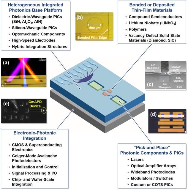
Journal of Physics: Photonics (2021) ###### Roadmap

PHOTONIC CIRCUIT INTEGRATED PLATFORMS
2 - Heterogeneous Integrated Photonics for Quantum Information Science and
Engineering
Paul W. Juodawlkis, William Loh, Cheryl Sorace-Agaskar
MIT Lincoln Laboratory

Status
Integrated photonic technologies will play a central role in advancing the frontiers of quantum
information science and in the full realization of quantum processing, sensing, and communication
applications. The required scaling (i.e., thousands to millions of quantum processing or sensing
elements) and functional complexity of these quantum systems will only be possible through the high
density, enhanced performance, and environmental stability afforded by photonic integrated circuits
(PICs). Photonic functions that will be needed include light generation (both uncorrelated photon
beams and entangled-photons), amplification, modulation, switching, routing and qubit input/output
(I/O) interfacing, passive splitting/combining, filtering, frequency translation, and detection (both
single photon and linear). Due to the distinct material properties required to realize these functions
over the operating wavelengths (i.e., ultraviolet to near-infrared) associated with the various quantum
modalities, it is highly unlikely that the required PICs can be made using a homogeneous material
platform such as silicon or a single compound-semiconductor material system. Therefore, advances in
quantum information science and engineering will require the development of heterogeneous
material PICs that are made available to the community through a collaborative ecosystem of design,
fabrication, packaging and evaluation resources.
 Figure 1 depicts a generic heterogeneous PIC platform that combines the fabrication process
control and yield of advanced silicon foundry toolsets with the wide-ranging materials options and
flexibility of post-silicon-fab hybrid
integration of materials and components.
The base platform is comprised of multi-
layer dielectric (i.e., silicon nitride (SiN),
alumina (Al2O3)) and silicon waveguides that
are used to implement passive (Fig 1(a)) [1]
and active components, and to create
optimized interfaces for heterogeneous
integration. Low optical losses have been
achieved in both medium-confinement
waveguides (< 0.2 dB/cm in SiN from 600-
1650 nm, 3 dB/cm in Al2O3 at 370 nm [2]) and
low-confinement waveguides (0.001 dB/cm
in SiN from 1300-1650 nm). Optical sources
and other non-silicon-based active devices
can be added through a combination of
material growth and deposition, layer
 Figure 1. Heterogeneous integrated photonic platform. Inserts depict
transfer, wafer bonding, and pick-and-place elements developed at MIT LL: (a) 3D beam profiles from multi-
techniques. Exemplar demonstrations of wavelength surface-grating lenses for trapped-ion illumination, (b)
 thin-film lithium niobate (TFLN) bonded to silicon-nitride ring
such a heterogeneous PIC platform include
 resonators, (c) InGaAsP/InP quantum-well membrane bonded to
high-power (> 300 mW) low-noise lasers silicon dioxide with InP regrowth, (d) flip-chipped semiconductor
incorporating flip-chipped semiconductor optical amplifiers, and (e) single-photon Geiger-mode avalanche
optical amplifiers (Fig. 1(d)) [3], surface- photodiodes (GmAPDs).
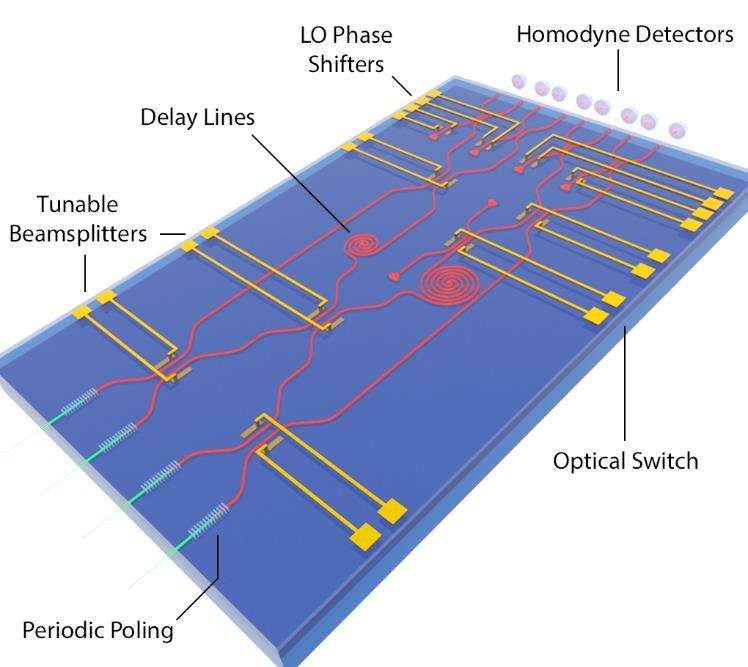
Journal of Physics: Photonics (2021) ###### Roadmap

bonded optical gain media (Fig. 1(c)) [4], [5], and low-loss surface-bonded thin-film lithium-niobate
(TFLN) waveguides (Fig. 1(b)) [6]. While this initial work along with the work of other photonic
developers are important first steps, a more significant and coordinated effort is required to develop
the platforms needed by the community.
Current and Future Challenges
The principal challenges to developing heterogeneous PICs for the quantum community are:

 • The breadth of the requirements across the different quantum modalities
 • The evolution of these requirements as the field transitions from fundamental scientific
 investigations to scaled engineering prototypes and products
 • The variety of photonic materials, devices, and integrated circuits needed to meet the
 requirements
 • The electronic-photonic integration needed to initialize and control the photonic functions,
 and to process, convert, and transfer the I/O information

We briefly address each of these principal challenges in the following paragraphs.

Breadth of requirements. The photonic functions and their associated requirements can be divided
into two major classes based on whether the photons serve as the qubits or if they are used to
interface to the physical qubit. Quantum systems based on photon qubits require sources of entangled
photons, ultralow optical propagation loss, control and maintenance of optical coherence, and high-
efficiency detection. For systems in which the photons serve as the I/O to the physical qubit, many of
the above requirements can be relaxed. However, other qubit-specific requirements, which will
depend on the physics of the photon-to-qubit coupling will be present. The need to operate at many
different wavelengths is also a challenge.

Evolution of requirements. The requirements of photonics in large-scale quantum systems are still
being defined as early demonstrations are performed. For example, consider trapped-ion-based
quantum systems for quantum computing and optical atomic clocks. As mentioned by Chiaverini et al.
in this issue [7], MIT LL has integrated SiN waveguides and vertical-grating lenses with ion-trap surface-
electrodes to deliver the six wavelengths required to perform qubit operations on a Sr+ ion (Fig. 1(a))
[1]. Significant challenges must be overcome to scale this architecture to the number of trapped ions
required for array-based optical atomic clocks and practical quantum computing. These include
waveguide loss, size and efficiency of the grating couplers, the lack of high-extinction optical switches
and frequency shifters having small enough size to be integrated at each trapped-ion site, crosstalk
due to scattered light in high-density PICs, fabrication yield and reproducibility, and the need for
integrated optical amplifiers, single-photon sensitive photodetectors (Fig. 1(e)), and electronics.
Equally difficult scaling challenges exist for other quantum modalities. One example is networking of
superconducting quantum processors via optical fiber interconnects that will require the development
of coherent microwave to optical photon conversion. Transition from the lab to the field will also
require improvements in environmental stability and packaging.

Variety of materials, devices, and integrated circuits. It will be very costly, both in terms of dollars and
time, to develop and maintain uncoordinated integrated photonics platforms to address the wide
range of photonic functions and operating wavelengths required across the quantum modalities (see
Status section above).
Journal of Physics: Photonics (2021) ###### Roadmap

Electronic-photonic integration. Most quantum photonic functions will require integration with
electronics to provide DC power, control, and I/O with the classical world. The level of integration
increases with the number and density of qubits to support the required interconnects. It will be
critical that this integration be implemented in a way that is both scalable and shields the quantum
elements from electromagnetic interference (EMI) generated by the electronics.

Advances in Science and Technology to Meet Challenges
To address the significant challenges to providing broadly applicable, scalable, and cost-effective
heterogeneous integrated photonics to the quantum community, the following advances will be
required:

 • A community-defined set of broad-wavelength (~0.35-2.0 μm), multi-waveguide-layer base
 platforms containing both core photonic devices and structures for implementing a range of
 heterogeneous photonic integration techniques (e.g., flip-chip bonding, surface bonding,
 epitaxial growth), and that are fabricated using silicon-foundry-compatible materials and
 processes well described by open process design kits (PDKs)
 • A variety of application-specific materials and devices that can be heterogeneously integrated
 onto the base platforms using either primary foundry or secondary hybrid-integration facilities
 • Three-dimensional (3D) integration with electronics using wafer-bonding techniques to
 decouple the photonic and electronic fabrication processes and to facilitate enhanced EMI
 shielding

Table 1 summarizes a number of key integrated photonic functions/devices, the challenges to
developing them, and the advances that will be required to meet the challenges. Several of the
challenges require material, fabrication and device advances to reduce optical loss, realize efficient
optical gain, and enable frequency translation over a wide spectral range. Scaling to large numbers of
on-chip gain elements is expected to require improvements in heteroepitaxial material growth and
integration with silicon [8] and dielectric waveguides. Comparable material and integration advances
will be required to realize high-rate, reproducible sources of single and entangled photons integrated
with low-loss waveguides for transmission and optical processing. Integration of nonlinear optical
materials such as surface-bonded TFLN for switches and frequency shifters will need to be scaled from
chip to wafer level. Silicon-foundry-compatible piezoelectric materials (e.g., AlN) will likely be required
in the base platform to implement electro-optomechanical resonators to enable coherent
transduction between microwave and optical photons. New materials and device concepts will also
be required to realize large arrays of optical switches having high extinction, low excess loss, and low
static power dissipation. Transitioning from the lab to the field will require low-cost, environmentally
robust subsystems such as ultra-narrow-linewidth lasers based on stimulated Brillouin scattering (SBS)
in optical fibers [9], [10] or ultralow-loss on-chip waveguides.

Concluding Remarks
The quantum community will benefit from a collaborative and coordinated effort to develop
heterogeneous PIC base platforms, materials, devices and circuits, flexible integration processes, and
advanced packaging techniques. Heterogeneous integration will be necessary due to the breadth of
the photonic requirements across the various quantum modalities, the evolution of these
requirements as the field matures, and the wide range of technologies needed to meet these evolving
requirements. The critical need for tight integration with electronics for control, processing, and I/O
will also eventually require 3D electronic-photonic integration. Enabling rapid progress in the field will
require cost-effective heterogeneous solutions that combine the existing silicon-foundry
Journal of Physics: Photonics (2021) ###### Roadmap

infrastructure with post-foundry integration of application-specific materials and devices at custom
hybrid-integration facilities.

 Table 1. Summary of some key integrated photonics functions, challenges, and required advances for quantum information science
 and engineering.
 Integrated Photonic
 Challenges Required Scientific and Technological Advances
 Functions / Devices
 • Develop low-loss materials and fabrication
 Low-Loss Waveguides in • Loss limits transmission and resonator Q techniques
 UV/Visible/Near-IR • Rayleigh scattering significant at visible/UV λ’s • Use low-confinement (Γ) for reducing
 scattering loss
 • Develop high-Γ ultralow-loss platform
 • Material loss limits achievable Q
 High-Q Resonators • Mature couplers to transition between low-Γ
 • Low-Γ resonators consume large area
 and high-Γ
 • Develop broadband III-V and solid-state gain
 • Multiple compound-semiconductor (III-V)
 Gain Media Covering media
 material systems needed to cover UV to near-
 UV/Visible/Near-IR • Use nonlinear frequency conversion to cover λ
 IR λ range
 gaps
 • Mature on-chip SBS lasers at visible and near-IR
 • Achieving required stability with compact
 Compact Lasers with Ultra- λ’s
 cavity
 Narrow Linewidth • Improve power conversion efficiency of III-V
 • Low power conversion efficiency limits scaling
 gain media
 • Mature on-chip SPDC sources having high
 • Entangled-photon generation rate too low
 efficiency
 Quantum Sources • Precise location of single-photon sources in
 • Develop and mature new materials (SiC, AlN,
 PICs
 diamond)
 • Acousto-optic frequency shifters are too large • Develop improved electro-optic materials and
 High-Efficiency Frequency
 • Low conversion efficiency between microwave devices
 Conversion
 and optical photons • Develop optomechanic quantum transducers
 • Required extinction (e.g., >70 dB for most • Develop materials and devices for non-
 Compact High-Extinction
 optically active qubits) difficult to achieve via interferometric switches (e.g., acousto-optic,
 Optical Switches
 interferometric switches electroabsorption)
 Low-Static-Power, Low- • Power of thermo-optic switches limits scaling • Develop improved materials and devices (e.g.,
 Loss Optical Switches • Loss of non-thermal switches limits scaling polymers, strain-induced χ(2), chalcogenides)
 • Geiger-mode APDs generate large EMI • Develop EMI shielding techniques
 Single-Photon Detectors • Superconducting detectors require low-K • Optimize heterogeneous PIC platform for low
 temps temps
 • Develop sub-wavelength photonic materials &
 • Required number (>106) of current photonic
 Very-Large Scale devices
 devices will require area >> stepper reticle
 Integration (VLSI) PICs • Develop wafer-scale lithography and fab
 area
 processes
 • Difference in photonic & electronic device
 • Mature wafer-bonded 3D integration
 Electronic-Photonic sizes
 incorporating metallic-electrode EMI shielding
 Integration • Proximity of photonics & electronics induces
 layers
 EMI

Acknowledgements
The authors gratefully acknowledge useful discussions with MIT LL colleagues John Chiaverini,
Siddhartha Ghosh, Christopher Heidelberger, Robert McConnell, and Danna Rosenberg. This material
is based upon work supported by the Under Secretary of Defense for Research and Engineering
(USDR&E), the United States Air Force, and the Defense Advanced Research Projects Agency (DARPA)
under Air Force Contract No. FA8702-15-D-0001. Any opinions, findings, conclusions or
recommendations expressed in this material are those of the author(s) and do not necessarily reflect
the views of the USDR&E, the United States Air Force and DARPA.

References
[1] R. J. Niffenegger, J. Stuart, C. Sorace-Agaskar, D. Kharas, S. Bramhavar, C. D. Bruzewicz, W.
Loh, R. T. Maxson, R. McConnell, D. Reens, G. N. West, J. M. Sage, and J. Chiaverini, “Integrated multi-
wavelength control of an ion qubit,” Nature, vol. 586, pp. 538-542, 2020.
Journal of Physics: Photonics (2021) ###### Roadmap

[2] C. Sorace-Agaskar, D. Kharas, S. Yegnanarayanan, R. T. Maxson, G. N. West, W. Loh, S.
Bramhavar, R. J. Ram, J. Chiaverini, J. Sage, and P. Juodawlkis, “Versatile silicon nitride and alumina
integrated photonic platforms for the ultraviolet to short-wave infrared,” IEEE J. Sel. Top. Quantum
Electron., vol. 25, pp. 1-15, 2019.
[3] D. Kharas, J. J. Plant, W. Loh, R. B. Swint, S. Bramhavar, C. Heidelberger, S. Yegnanarayanan,
and P. W. Juodawlkis, “High-power (> 300 mW) on-chip laser with passively aligned silicon-nitride
waveguide DBR cavity ” IEEE Photonics Journal, v. 12, pp. 1-13, 2020.
[4] R. B. Swint, S. J. Spector, C. L. Chen, J. J. Plant, T. M. Lyszczarz, and P. W. Juodawlkis,
“Waveguide engineering for hybrid Si / III-V lasers and amplifiers,” in Proc. Conference on Lasers and
Electro-Optics (CLEO), 2012, pp. paper CTu2N.7.
[5] C. Heidelberger, C. T. Santis, J. J. Plant, E. M. Morissette, D. Kharas, R. B. Swint, A. Yariv, and
P. W. Juodawlkis, “InGaAsP/InP membrane gain sections for III-V/SiNx heterogeneous photonic
integration,” in Proc. Conference on Lasers and Electro-Optics (CLEO), 2021.
[6] S. Ghosh, S. Yegnanarayanan, M. Ricci, D. Kharas, and P. Juodawlkis, “Low-loss thin-film
lithium niobate bonded on silicon nitride waveguides,” in Proc. Conference on Lasers and Electro-
Optics (CLEO), 2020, pp.
[7] K. K. Mehta and J. Chiaverini, “Photonic integration of trapped ions,” Journal of Physics:
Photonics, vol.?, pp.??-??, 2021.
[8] J. Klamkin, L. Wang, B. Song, B. Shi, S. S. Brunelli, and T. Meissner, “Lasers on silicon by
heteroepitaxy,” in Proc. IEEE Photonics Conference (IPC), 2020.
[9] W. Loh, S. Yegnanarayanan, F. O’Donnell, and P. W. Juodawlkis, “Ultra-narrow linewidth
Brillouin laser with nanokelvin temperature self-referencing,” Optica, vol. 6, pp. 152-159, 2019.
[10] W. Loh, J. Stuart, D. Reens, C. D. Bruzewicz, D. Braje, J. Chiaverini, P. W. Juodawlkis, J. M. Sage,
and R. McConnell, “Operation of an optical atomic clock with a Brillouin laser subsystem,” Nature, vol.
588, pp. 244-249,, 2020.
Journal of Physics: Photonics (2021) ###### Roadmap

3 - Heterogeneous Integration Methods with III-V Quantum Dots
Marcelo Davanco, National Institute of Standards and Technology
Status
Heterogeneous integration encompasses bonding of two dissimilar materials followed by device
fabrication in a single process flow. The approach has been applied in the fabrication of optoelectronic
[Bowers2019] and nonlinear photonic [Moody2020] devices on silicon substrates and on-chip
waveguides, with gain, absorption and enhanced optical nonlinearities provided by III-V
semiconductor materials. While much of the initial work involved bonding at the chip scale, bonding
at the wafer scale was later also demonstrated [Liang 2010]. Heterogeneous integration at the chip
scale was used by Ben Bakir et al. [BenBakir2006] to produce, for the first time, optically pumped
lasers based on III-V epitaxial quantum dots on a silicon substrate. Further progress led to
demonstration of electrically injected quantum dot lasers on silicon [Tanabe2012]. In 2017, the
approach was used at the chip scale to produce Si3N4-based photonic circuits with integrated single-
photon sources based on single InAs quantum dots [Davanco2017]. Whereas devices in this work
contained multiple, randomly positioned quantum dots, deterministic fabrication of single-photon
sources with quantum dots precisely located within GaAs nanowaveguides were demonstrated in
2019 by Schnauber, et al. [Schnauber2019]. This later work also showed triggered and post-selected
indistinguishable single-photon emission into Si3N4 waveguides, with reported coherence lengths
comparable to those obtained from InAs self-assembled quantum dots in GaAs-only devices, under
similar optical pumping conditions. The introduction of single quantum dots in quantum silicon
photonic circuits has the potential to greatly scale integrated quantum photonic information systems
that rely on probabilistic gates, which generally require highly efficient single-photon qubit
generation, low-loss waveguide interferometric networks, and highly efficient single-photon
detection. On-chip single quantum dots may act as triggered, high-rate sources of indistinguishable
photons, and can couple with high efficiency to the silicon photonic circuit through carefully designed
GaAs nanophotonic structures. Single quantum dots strongly coupled to on-chip cavities furthermore
offer a path towards single-photon nonlinearities, which could enable deterministic quantum gates
on chip [Kim2016]. It is worth noting that hybrid integration techniques, in which III-V and silicon-
based devices are produced in separate runs and then brought together through methods such as
pick-and-place or transfer-printing, have also successfully produced silicon photonic devices with on-
chip quantum dot single-photon sources [Elshaari2020].

Current and Future Challenges
Deterministic fabrication of on-chip devices with functionality based on single epitaxial quantum dots
currently poses a formidable challenge towards scalable integration. Single-dot device functionality
requires the creation of an efficient interface between a single quantum dot and a single, efficiently
accessible, spatially confined optical mode – e.g., a cavity resonance or waveguide mode. This in turn
requires positioning the single dot with sub-wavelength-scale precision at specific locations within the
extent of the spatial optical mode, in order to maximize coupling. While site-selective quantum dot
growth techniques have allowed such an achievement [Sunner2008], self-assembled quantum dots
produced via the Stranski-Krastanow (S-K) growth mode have generally demonstrated superior
coherence, a critical characteristic for quantum photonic applications. In contrast with site-controlled
dots, self-assembled quantum dots are produced at random positions across the growth wafer
surface, and generally present a wide heterogeneity of optical properties such as transition energies,
quantum yield and coherence times. Deterministic fabrication of a single S-K dot device, then, requires
first that an individual emitter with the desirable optical properties be identified within largely
heterogeneous, as-grown ensemble. Subsequently, the photonic geometry that supports the desired,
interfacing optical mode must be fabricated around the identified quantum dot. It is worth noting that
Journal of Physics: Photonics (2021) ###### Roadmap

such challenges exist for any device that derive their functionality from single quantum emitters, in
both homogeneous and heterogeneous material platforms, and in hybrid and heterogenous
fabrication approaches.

Advances in Science and Technology to Meet Challenges
Advances in site-selective growth to allow better control of quantum dot spectral homogeneity and
coherence properties would significantly improve integration scalability, by allowing deterministic
single quantum dot device fabrication through standard, scalable top-down processing techniques. In
the absence of such possibility, scalable integration of single S-K quantum dot devices would greatly
benefit from the development of high-throughput single-quantum dot localization and spectroscopy
systems. Ideally, such a system would allow fast identification of large number of dots emitting
indistinguishable single-photons at desired wavelengths, for integration with nanophotonic
geometries. Because S-K quantum dots occur at random locations, however, such an approach would
result in randomly located single-dot devices. These devices would then have to be connected to the
photonic circuit through ad hoc routes, which cannot be produced predictably with optical projection
lithography. Hybrid integration techniques can in principle circumvent such issues, since prefabricated
quantum dot devices (even if produced at random locations on the origin chip) can be deterministically
placed onto pre-determined locations on the destination chip. Scalable integration would, however,
require high throughput device transfer techniques, which may be challenging depending particularly
on alignment tolerances.

Concluding Remarks
In summary, heterogeneous integration has considerable potential for large-scale quantum silicon
photonic circuits with functionality based on single III-V semiconductor quantum dots. Although the
approach in principle allows completely top-down processing, integration scalability is principally
hampered by the necessity to locate and analyse quantum dots at an individual level prior to
fabrication. Importantly, though, such non-trivial and time-consuming tasks are generally necessary
in any integration platform for devices that employ single quantum emitters.

References
[Bowers2019] - J. E. Bowers et al., “Realities and Challenges of III-V/Si Integration
Technologies,” in 2019 Optical Fiber Communications Conference and Exhibition (OFC), Mar.
2019, pp. 1–3.
[Liang2010] – D. Liang et al., “Uniformity study of wafer-scale InP-to-silicon hybrid
integration”, Applied Physics A 103, 213 (2011).
[Tanabe2012] - K. Tanabe, D. Guimard, D. Bordel, S. Iwamoto, and Y. Arakawa, “Electrically
pumped 1.3 μm room-temperature InAs/GaAs quantum dot lasers on Si substrates by metal-
mediated wafer bonding and layer transfer,” Opt. Express, OE, vol. 18, no. 10, pp. 10604–
10608, May 2010, doi: 10.1364/OE.18.010604.
[Moody2020] - G. Moody, L. Chang, T. J. Steiner, and J. E. Bowers, “Chip-scale nonlinear
photonics for quantum light generation,” AVS Quantum Sci., vol. 2, no. 4, p. 041702, Oct.
2020, doi: 10.1116/5.0020684.
[BenBakir2006] - B. B. Bakir et al., “Room-temperature InAs/InP Quantum Dots laser
operation based on heterogeneous ‘2.5 D’ Photonic Crystal,” Opt. Express, OE, vol. 14, no. 20,
pp. 9269–9276, Oct. 2006, doi: 10.1364/OE.14.009269.
Journal of Physics: Photonics (2021) ###### Roadmap

[Davanco2017] - M. Davanco et al., “Heterogeneous integration for on-chip quantum
photonic circuits with single quantum dot devices,” Nature Communications, vol. 8, no. 1, p.
889, Oct. 2017, doi: 10.1038/s41467-017-00987-6.
[Schnauber2019] - P. Schnauber et al., “Indistinguishable Photons from Deterministically
Integrated Single Quantum Dots in Heterogeneous GaAs/Si3N4 Quantum Photonic Circuits,”
Nano Lett., vol. 19, no. 10, pp. 7164–7172, Oct. 2019, doi: 10.1021/acs.nanolett.9b02758.
[Kim2016] - H. Kim, R. Bose, T. C. Shen, G. S. Solomon, and E. Waks, “A quantum logic gate
between a solid-state quantum bit and a photon,” Nat Photon, vol. 7, no. 5, pp. 373–377, May
2013, doi: 10.1038/nphoton.2013.48.
[Elshaari2020] - A. W. Elshaari, W. Pernice, K. Srinivasan, O. Benson, and V. Zwiller, “Hybrid
integrated quantum photonic circuits,” Nat. Photonics, vol. 14, no. 5, pp. 285–298, May
2020, doi: 10.1038/s41566-020-0609-x.
[Sunner2008] - T. Sünner et al., “Scalable fabrication of optical resonators with embedded
site-controlled quantum dots,” Opt. Lett., OL, vol. 33, no. 15, pp. 1759–1761, Aug. 2008, doi:
10.1364/OL.33.001759.
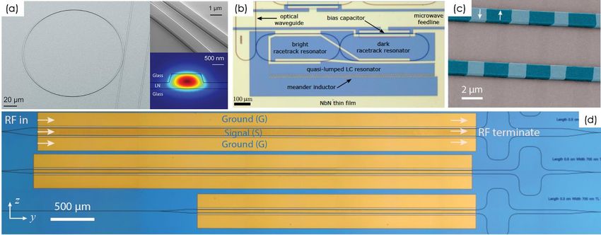
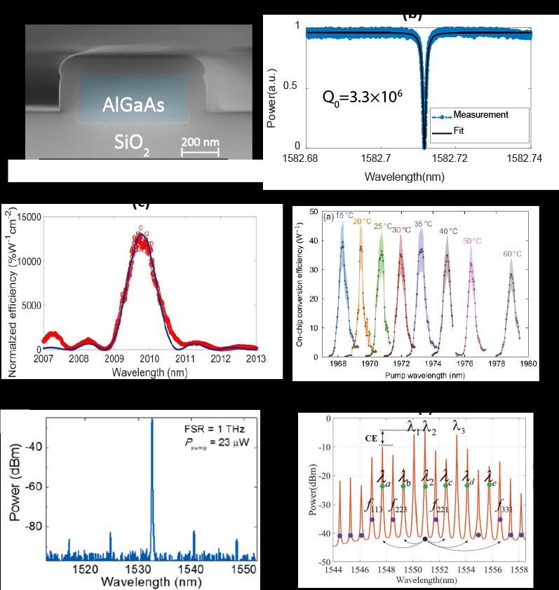
Journal of Physics: Photonics (2021) ###### Roadmap

4 - AlGaAsOI Integrated Quantum Photonics
Lin Chang, John E. Bowers, Galan Moody, Department of Electrical and
Computer Engineering, University of California, Santa Barbara, CA 93106, USA

Status
A primary goal in quantum photonics is the construction of fully integrated and versatile quantum
photonic circuits comprising tunable classical and quantum light sources, active and passive
components, programmable networks, and detectors [1], [2]. Over the last decade, remarkable
progress along this direction has been achieved on the silicon-on-insulator (SOI) platform, which
leverages the mature manufacturing infrastructure of the semiconductor industry for high volume and
low-cost production. To further extend the capabilities beyond what silicon can offer, a variety of
material candidates, such as silicon nitride, lithium niobite (LiNbO3), and III-V semiconductors have
been developed and investigated. Among the diverse photonic platforms, (aluminium) gallium
arsenide [(Al)GaAs] on insulator has attracted significant interest recently [3], [4] due to its direct
bandgap structure for light generation, large bandgap minimizing two-photon absorption at telecom
wavelengths, and large (2) and (3) optical nonlinear coefficients, which are orders of magnitude
higher than commonly used dielectric photonic media.

Traditionally, III-V photonic platforms suffered from high waveguide loss and low optical confinement
because all of the devices were processed on a native III-V substrate [5]. (Al)GaAs-on-insulator
[(Al)GaAsOI] overcomes this constraint by heterogeneously integrating an (Al)GaAs film with an
oxidized Si substrate by wafer bonding technology (Fig.1a). The high index contrast attained by this
approach brings a plethora of new opportunities in nonlinear and quantum applications by enhancing
the light intensity and tailoring the waveguide geometry. Another key advance for this platform is the
significant reduction in waveguide loss. By combining optimized lithography, etching, and passivation,
the propagation loss of AlGaAsOI waveguides ( 40,000% W-1cm-2 has been attained in a GaAsOI waveguide
(Fig.1d) [7]. For (3)-based nonlinear processes, a record-low threshold around 20 µW for Kerr comb
generation is achieved in a high-Q AlGaAsOI resonator (Fig.1e) [6], where the AlGaAs material bandgap
is engineered to avoid two photon absorption at the telecom band. Similar types of waveguides are
also used for efficient wavelength conversion in optical signal processing (Fig.1f) [8] with pump power
compatible with integrated laser sources.

Such high-efficiency nonlinear processes are essential for multiple quantum purposes. A recent
milestone with AlGaAsOI quantum photonics is the demonstration of entangled photon pair
generation from a microresonator through spontaneous four-wave-mixing (SFWM) [9]. Combining the
high Q-factor and the strong Kerr coefficient, a waveguide-integrated source exhibits a pair-generation
rate greater than 20 х 109 pairs sec-1 mW-2 near 1550 nm, with a heralded single photon purity > 99%,
entanglement visibility > 97% and coincidence-to-accidental ratio (CAR) > 4300. The brightness of this
source (2 х 1011 pair sec-1 mw-2 GHz-1 bandwidth) is about 1000-fold higher compared to traditional on-
chip entangled-pair sources. Such high-efficiency and high-quality quantum light sources in AlGaAsOI
Journal of Physics: Photonics (2021) ###### Roadmap

 points towards exciting prospects for
 combining state-of-the-art nonlinear
 components into the quantum regime
 and can potentially benefit a wide
 range of system-level applications.

 Current and Future Challenges

 Due to its short history, (Al)GaAsOI
 requires significant research and
 development in order to reach a
 similar level of integration as current
 quantum photonic circuits on silicon.
 Compared to the rich library of
 process design kits based on SOI
 waveguides, so far very few devices
 using (Al)GaAsOI have been
 developed to realize the necessary
 components in PICs, such as
Figure 1. Demonstrations on (Al)GaAsOI platform. (a) SEM image of the cross wavelength demultiplexing, Mach-
section of an AlGaAsOI waveguide. (b) Transmission spectrum of an AlGaAs
 Zehnder interferometers,
resonator. The extracted Q is 3.3 х 106. (c) The transfer function of SHG
normalized efficiency for a GaAsOI waveguide. (d) SHG spectrums under different modulators, and detectors. One
temperatures by a GaAsOI waveguide, whose normalized efficiency is > 40,000 % challenge that must be overcome to
W-1cm-2. (e) The generated frequency comb lines from an AlGaAs resonator under
23 µW power. (f) Frequency conversion for communication experiment by an
 support the growth of (Al)GaAsOI
AlGaAsOI waveguide. technology is to transition from
 research development level
fabrication to commercial vendors and/or foundries. Another potential challenge for the scalability of
this platform is the cost of III-V materials, which is one of the key advantages that silicon photonics
holds over traditional native III-V platforms.

Advances in Science and Technology to Meet Challenges

Due to the exemplary properties of III-V semiconductors for photonics, plentiful functions can be
implemented on the (Al)GaAsOI platform for quantum applications. Besides following the route of SOI
in standardizing the basic passive components, (Al)GaAsOI provides several prospective advantages
for the monolithic integration of active and passive components. In terms of quantum light sources,
the large (2) nonlinearity can lead to entangled and single-photon generation based on spontaneous
parametric down-conversion (SPDC), which is expected to be even more efficient compared to SFWM,
further easing the pump power requirements. Similarly, producing squeezed optical states—another
essential resource for quantum optical information processing in the continuous variable regime—can
be realized via either the (2) or (3) nonlinearities. In addition to the nonlinear processes, one key
feature of the material system of (Al)GaAs and its alloys is the compatibility with InAs/GaAs quantum
dots (QDs), which can be used for generating on-demand single photons and for achieving single-
photon nonlinearities.

By leveraging III-V quantum well (QW) or QD epitaxial layers, electrically pumped lasers can be directly
integrated along with the passive circuits on (Al)GaAsOI, which can serve as a tunable pump for
Journal of Physics: Photonics (2021) ###### Roadmap

 quantum light generation and an
 on-chip local oscillator for
 interferometry. The existence of the
 electro-optic and piezo-electric
 effects potentially can enable high-
 speed modulators with low
 insertion loss. Importantly, those
 modulators are suitable to work
 under cryogenic temperature,
 which are required for operating
 QD-based single photon emitters as
 Figure 2. Concept of fully integrated quantum photonic chips based on AlGaAsOI. well as superconducting nanowire
 single-photon detectors (SNSPDs),
which recently has also been successfully integrated on GaAs waveguides [10]. Therefore, a route
exists to fully integrated quantum PICs by monolithically integrating all those functions onto
(Al)GaAsOI, as shown in Fig.2.

To further improve the scalability, (Al)GaAsOI can be heterogeneously integrated onto SOI PICs to
harness large-scale CMOS compatible production. Another strategy to lower the cost of III-V materials
is direct epitaxial growth on Si wafers instead of native III-V substrates. Remarkable advances have
been made along this direction for the (Al)GaAs material system, whereby the film qualities are
comparable with layers on GaAs native substrates.

Concluding Remarks

With the remarkable performance of quantum light sources and the convenience of system-level
integration, rapid growth of research in (Al)GaAsOI for integrated quantum photonics is expected. The
efficiencies of current nonlinear devices will be further improved, and novel capabilities will be
enabled by exploring different properties of the material system. The simultaneous realization of
lasers, quantum light sources, modulators, and photodetectors will be the next key steps to
accomplish fully integrated quantum photonics with this platform. These developments will also
benefit other applications in integrated photonics and it will enable a wide range of new opportunities
in classical and quantum computing, communications, and sensing.

Acknowledgements
We gratefully acknowledge support via the UC Santa Barbara NSF Quantum Foundry funded via the
Q-AMASE-i program under award DMR-1906325. G.M. acknowledges support from AFOSR YIP Award
No. FA9550-20-1-0150 and the National Aeronautics and Space Administration under Subcontract No.
UCSB-01 and Amethyst Research, Inc.

References
[1] J. Wang, F. Sciarrino, A. Laing, and M. G. Thompson, “Integrated photonic quantum
 technologies,” Nat. Photonics, vol. 14, no. 5, pp. 273–284, 2020, doi: 10.1038/s41566-019-
 0532-1.
[2] G. Moody, L. Chang, T. J. Steiner, and J. E. Bowers, “Chip-scale nonlinear photonics for quantum
 light generation,” AVS Quantum Sci., vol. 2, no. 4, p. 041702, Dec. 2020, doi:
 10.1116/5.0020684.
[3] M. Pu, L. Ottaviano, E. Semenova, and K. Yvind, “Efficient frequency comb generation in
 AlGaAs-on-insulator,” Optica, vol. 3, no. 8, p. 823, Aug. 2016, doi: 10.1364/OPTICA.3.000823.
Journal of Physics: Photonics (2021) ###### Roadmap

[4] L. Chang et al., “Ultra-efficient frequency comb generation in AlGaAs-on-insulator
 microresonators,” Nat. Commun., vol. 11, no. 1, pp. 1–8, Dec. 2020, doi: 10.1038/s41467-020-
 15005-5.
[5] L. Chang et al., “Heterogeneously integrated GaAs waveguides on insulator for efficient
 frequency conversion,” Laser Photon. Rev., 2018, doi: 10.1002/lpor.201800149.
[6] W. Xie et al., “Ultrahigh-Q AlGaAs-on-insulator microresonators for integrated nonlinear
 photonics,” Opt. Express, vol. 28, no. 22, p. 32894, 2020, doi: 10.1364/OE.405343.
[7] E. J. Stanton et al., “Efficient second harmonic generation in nanophotonic GaAs-on-insulator
 waveguides,” Opt. Express, vol. 28, no. 7, pp. 9521–9532, 2020, doi: 10.1364/OE.389423.
[8] J. Qin et al., “On-chip high-efficiency wavelength multicasting of PAM3/PAM4 signals using
 low-loss AlGaAs-on-insulator nanowaveguides,” Opt. Lett., vol. 45, no. 16, p. 4539, Aug. 2020,
 doi: 10.1364/ol.398777.
[9] T. J. Steiner et al., “Ultra-bright entangled-photon pair generation from an AlGaAs-on-insulator
 microring resonator,” Sep. 2020 [Online]. Available: http://arxiv.org/abs/2009.13462.
[10] C. McDonald et al., “III-V photonic integrated circuit with waveguide-coupled light-emitting
 diodes and WSi superconducting single-photon detectors,” Appl. Phys. Lett., vol. 115, no. 8, p.
 081105, Aug. 2019, doi: 10.1063/1.5108893.
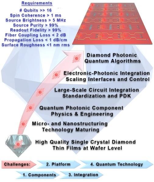
Journal of Physics: Photonics (2021) ###### Roadmap

5 – Integrated Quantum Photonics in Diamond
Niels Quack (EPFL), Christophe Galland (EPFL), Igor Aharonovich (UTS)
Status
The unique combination of extraordinary physical and optical properties of high-purity single crystal
diamond has propelled this material far beyond its traditional use as gemstone in jewellery, fostering
a growing body of scientific research in the field of diamond photonic integrated circuits (PICs) [1].
While PICs made of silicon or III-V materials have reached commercial applications, e.g. in
telecommunications and interconnects, quantum PICs are still in their infancy [2]. They notably require
on-demand generation of indistinguishable single photons, low-loss optical signal routing, on-chip
single photon manipulation and detection, and engineering of specific quantum functionalities, such
as quantum registers or quantum memories [3]. In this context, diamond’s ability to host
paramagnetic, optically active atomic defects [4], such as the nitrogen-vacancy colour centre [5], has
led to its widespread recognition as a promising material for quantum information processing [6].
Diamond PICs have the potential to host large arrays of long-coherence electronic and nuclear spin
qubits linked by flying photonic qubits and coherently controlled by microwave circuits [7]. In addition,
diamond’s unrivalled mechanical properties makes it promising for cavity quantum optomechanics,
which provides additional opportunities for implementing quantum coherent frequency conversion
and quantum memories in a same platform [8]. As an almost ideal quantum photonic material,
diamond holds the promise to combine in a single platform all the required components for large-
scale quantum PICs with the potential to operate at ambient temperature. To date, an impressive
collection of experiments has been realized at the individual component level [9]. This progress has
been enabled by the advances in chemical vapour deposition (CVD) growth of single crystal diamond
with the level of purity and low defect density required for quantum photonics, and by advances in
micro- and nanofabrication, allowing for precision shaping of diamond at the nanoscale [10]. This
 advancement has recently led to several small scale quantum
 photonic circuit demonstrations, using hybrid integration of
 diamond with other photonic material platforms [11]. However,
 despite these recent achievements, large-scale diamond quantum
 PICs, with thousands or millions of individual components, remain
 elusive. This roadmap aims at outlining the requirements for
 establishing such a platform.

 Current and Future Challenges
 In order to establish mature and scalable diamond quantum PICs,
 several challenges need to be addressed, which can be divided into
 four major areas, namely (1) components, (2) platform, (3)
 integration, and (4) quantum technology. Over the past decade, an
 abundance of individual components for integrated diamond
Figure 1. The outstanding material properties photonics has been investigated in academic research. For
of single crystal diamond motivates the
development of large-scale diamond
 example, grating couplers, waveguides, phase shifters, power
quantum photonic integrated circuits hosting couplers, cavities, optomechanical resonators, single photon
a wealth of quantum photonic components. sources, light emitting diodes, Raman laser, supercontinuum
 generation and detectors have all been demonstrated. These
components have to be matured and their operation optimized for a selected wavelength range; for
scalable quantum operation, their insertion loss has to be drastically reduced; finally, they must be
combined into a standardized technology. The component-level challenges go naturally hand in hand
with the establishment of a platform technology. Building on high quality thin film single crystal
diamond as the photonic layer, a manufacturing process flow needs to be developed that can host at
You can also read