Cost-Competitive, High-Performance, Highly Reliable Power Devices on Silicon Carbide
←
→
Page content transcription
If your browser does not render page correctly, please read the page content below

Cost-Competitive, High-Performance,
 Highly Reliable Power Devices on
          Silicon Carbide
                          Principal Investigators: Woongje Sung
                  State University of New York Polytechnic Institute
                              2021 DOE Annual Merit Review

This presentation does not contain any proprietary, confidential, or otherwise restricted information.

                                                                                          Project ID # elt247
                                                                              SUNY POLYTECHNIC INSTITUTE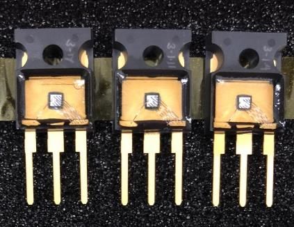
Overview
            Timeline                                        Barriers

   •   Project start April 2019          •    Cost: the lack of device innovations
                                              and processing technologies
   •   Project end March 2024            •    Performance: need state-of-the-art f
   •   Percent Complete: 40%                  acility for tight design rules
                                         •    Reliability and ruggedness: trade off
                                              relationship with performance
             Budget
   •   BP2 total $333K: Federal $ 300K                      Partners
       + cost share (10%)                •    Sandia National Laboratories
                                         •    The Ohio State University
                                         •    Virginia Tech

                                             2020 IEEE International
                                                                SUNY Reliability
                                                                      POLYTECHNICPhysics INSTITUTE
                                                                                         Symposium   22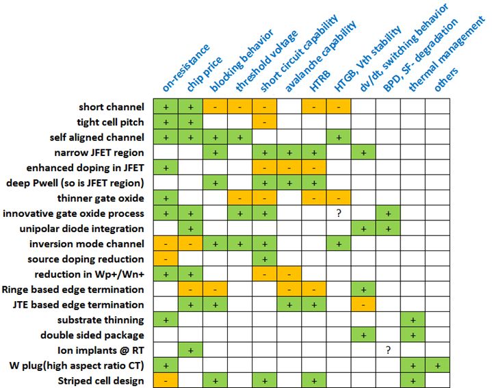
Relevance – objectives / impact
 Overall objectives in this project
  •   The primary objective of this project is to ensure that the next-generation of wide-bandgap devi
      ces of sufficient performance, reliability, and price to achieve the system-level DOE goals.

 Objectives in previous period (BP2, FY2020-2021)
  •   Establishment of the process baseline for Gen2 MOSFETs.
  •   Evaluation of Gen2 MOSFETs;
           Performance; Ron,sp=5mohm-cm2, Vth=2V, BV=1600V.
           Reliability and Ruggedness; Short Circuit SOA 2µs

 Impact of research
  •   The successful development of the proposed device will bring in a highly efficient and reliable
      power electronics for electric drive trains.

                                                      2020 IEEE International
                                                                         SUNY Reliability
                                                                               POLYTECHNICPhysics INSTITUTE
                                                                                                  Symposium   33
Milestones – BP3
           Milestone               Type                              Description
                                              The cell and edge termination structures for MOSFETs and JBS
       Gen3 SiC MOSFET
                                  Technical          diode integrated MOSFETs have been optimized;
            design
                                                     Optimized devices included in a single mask-set.
       Gen3 SiC MOSFETs                       Two engineering lots to make Gen3 devices completed; Implants
                                  Technical
            fabrication                         conducted at RT; Self-aligned channel scheme optimized.
       Gen3 SiC MOSFETs                           Static performances have been characterized on-wafer;
                                  Technical
            evaluation                                    Reliabilities and ruggedness evaluated.
        AlGaN/GaN HEMT
        device processing         Technical        Various stages of devices processing are completed.
           optimization
                                                     Performances of Gen3 SiC MOSFETs evaluated:
   Improved static performance,
                                                       BV = 1700V, Ron,sp = 4 mohm-cm2, Vth = 2V
      Reliability assessment      Go/No Go
                                                                 Short Circuit SOA 4µs;
        on Gen3 devices
                                                  Tests on TDDB, HTGB, HTRB, dv/dt, 3Q diode behavior

                                                         2020 IEEE International
                                                                            SUNY Reliability
                                                                                  POLYTECHNICPhysics INSTITUTE
                                                                                                     Symposium   44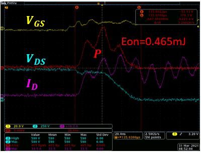
Approach – CPR metrics

                         2020 IEEE International
                                            SUNY Reliability
                                                  POLYTECHNICPhysics INSTITUTE
                                                                     Symposium   55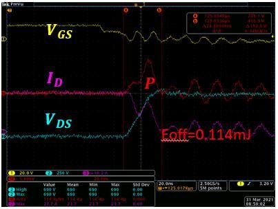
BP1-MOSFETs
Technical Accomplishments and Progress
                                                                        Top Metal

                                                                                ILD
                                                                                                        Poly-Si
                                                                        ohmic                              Gox
                                                                                N+                Ch
                                                                                      P-well           JFET

                                                                                      N- Drift layer

                                                                                      N+Substrate
                                                                                          Drain

    6 inch SiC wafer                     Packaged SiC MOSFETs                Cross-sectional view                         SEM image

              Transfer characteristics                          Output characteristics                            Blocking behaviors

                                                                                    2020 IEEE International
                                                                                                       SUNY Reliability
                                                                                                             POLYTECHNICPhysics INSTITUTE
                                                                                                                                Symposium       66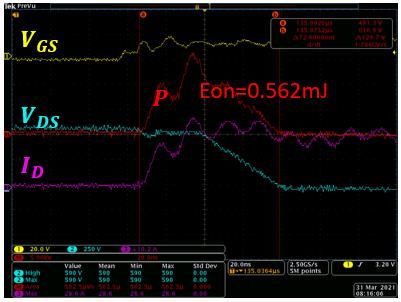
BP1-MOSFETs
Technical Accomplishments and Progress
                                                                                                                                     Avalanche energy=665mJ

                                                                                                                                                               Test conditions
                                                                                                                                                                  VDC: 100V
   Body diode degradation                           PBTI: Vgs=+20V                          NBTI: Vgs=-10V                                Avalanche energy         L: 11mH

                                                                                         Channel length=0.5um                             Channel length=1.0um

    Switching Turn-on                              Switching Turn-off                    Short-circuit capability                          Short-circuit capability
                Test condition: Resistor=10 ohm,                                                             Test condition: Vgs=20V, Vds=800V.
                 Vgs=15V, Vds=~600V Id=~22A.
                                    Body diode, BTI, Avalanche, and SC were measured at OSU, Switching was measured at VT

                                                                                       2020 IEEE International
                                                                                                          SUNY Reliability
                                                                                                                POLYTECHNICPhysics INSTITUTE
                                                                                                                                   Symposium                                77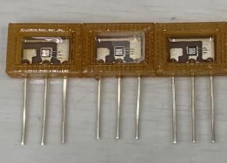
BP1-MOSFETs
Technical Accomplishments and Progress

  Packaged SiC MOSFETs for HT operation                     Output characteristics (Ron,sp)                                   Blocking behaviors

                                                                                                                                  Test condition: Resistor=10 ohm,
                                                                                                                                   Vgs=15V, Vds=~600V Id=~22A.
                                      Switching Turn-on at 210 oC                              Switching Turn-off at 210 oC
                                                              VT packaged and measured MOSFETs

                                                                                        2020 IEEE International
                                                                                                           SUNY Reliability
                                                                                                                 POLYTECHNICPhysics INSTITUTE
                                                                                                                                    Symposium                        88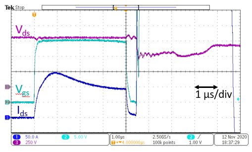
BP2-Mask design
Technical Accomplishments and Progress

• Mask design – floor plan for 1st and 2nd lot

•   PiN diode, JBS diode, MOSFETs (different
    sizes), JBSFETs and test structures were
    included.
•   Mask design was taped out – design review
    by SiCamore engineers, kerf (process
    monitoring boxes) insertion was completed.

                                                 BP2-lot1                              BP2-lot2

                                                  2020 IEEE International
                                                                     SUNY Reliability
                                                                           POLYTECHNICPhysics INSTITUTE
                                                                                              Symposium       99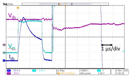
BP2-MOSFETs
Technical Accomplishments and Progress
                 Lch=0.5um with Nominal Pwell                                     Lch=0.5um with Deep Pwell

     Output characteristics            Blocking behaviors        Output characteristics                Blocking behaviors

                  Lch=0.3um with Deep Pwell

     Output characteristics            Blocking behaviors    Summary of Nominal Pwell             Summary of Deep Pwell

                                                            2020 IEEE International
                                                                               SUNY Reliability
                                                                                     POLYTECHNICPhysics INSTITUTE
                                                                                                        Symposium              1010
Summary
Ron,sp BV Body diode Avalanche Switching
PBTI/NBTI SC SOA
(on-wafer) (on-wafer) degradation energy Turn-on/Turn-off
3.24 Δ+0.45V/ 0.562/
1610V No degradation 665mJ >4us
moho-cm2 Δ-0.45V 0.110mJ
• Reliability and ruggedness tests were conducted on packaged devices from BP1 at RT and HT.
• The first lot in BP2 was completed; the 2nd lot is running at SiCamore.
• The static performance was significantly improved using deep Pwell structure.
• All aspects (CPR) need to be considered in a comprehensive research program.
• Strong team (fab and partner) was formed to accomplish the proposed goals.
SUNY POLYTECHNIC INSTITUTE 11Cost-Competitive, High-Performance,
Highly Reliable Power Devices on
Gallium Nitride
Principal Investigators: Shadi Sadvik
State University of New York Polytechnic Institute
2021 DOE Annual Merit Review
This presentation does not contain any proprietary, confidential, or otherwise restricted information.
Project ID # elt247
SUNY POLYTECHNIC INSTITUTEProgress: Processing Optimization and Breakdown Dependence
on Substrate Si Substrate Sapphire Substrate
0.25 0.40
Output Vgs=2V 0.35 Output Vgs=2 V
0.20 Vgs=1 V
Vgs=1V 0.30
Vgs=0 V
Ids (A/mm)
Ids (A/mm)
0.15 Vgs=0V 0.25
Vgs=-1 V
Vgs=-1V 0.20
Vgs=-2 V
0.10 Vgs=-2V 0.15
Vgs=-3 V
Vgs=-3V 0.10 Vgs=-4 V
0.05
Vgs=-4V 0.05 Vgs=-5 V
0.00
Unoptimized Etch
0.00 Vgs=-5V
0 5 10 15 20 0 5 10 15 20
Vds (V) Vds (V)
1.0E+00 1.0E+00
1.0E-01 Transfer 1.0E-01 Transfer
1.0E-02 1.0E-02
Ids (A/mm)
Ids (A/mm)
1.0E-03 1.0E-03
1.0E-04 1.0E-04
1.0E-05 1.0E-05
1.0E-06 1.0E-06
Vds=11V Vds=11V
1.0E-07 1.0E-07
Optimized Etch -10 -8 -6 -4 -2 0 2 -10 -8 -6 -4 -2 0 2
Vgs (V) Vgs (V)
1.E+00 1.E+00
1.E-01 Off-state Breakdown 1.E-01 Off-state Breakdown
• Poor device performance be due to unoptimized etch 1.E-02
I_drain (A/mm)
1.E-02
I_drain (A/mm)
condition resulting in poorly defined mesa sidewalls 1.E-03 1.E-03
Destructive
Devices fabricated with optimized process resulted in
1.E-04
• Breakdown
1.E-04
1.E-05 1.E-05
low leakage and ION/IOFF > 105 1.E-06 1.E-06
• Devices fabricated on Si substrate showed off-state 1.E-07 1.E-07
0 100 200 300 400 500 600 700 800 900
breakdown 2x higher than devices fabricated on sapph
0 100 200 300 400 500 600 700 800 900
V_drain (V) V_drain (V)
ire substrate, at ~800V.
13Technical Progress Summary and Future Work
• Improved etch process for mesa isolation drastically reduced leakage and improved gate control of
fabricated HEMT devices
• Devices fabricated at the same time on Si and sapphire substrates demonstrated strong gate control
and ION/IOFF > 105
• Devices fabricated on Si substrate demonstrated off-state breakdown voltage ~800 V
• Semi-insulating bulk GaN substrates have been received
• New MOCVD carrier platter for 1.5” GaN substrates was been designed, ordered and received.
• Optimized HEMT growth and fabrication process will be performed on SI GaN substrates. Comparative
device measurements and reliability testing will be conducted
14You can also read