Photonics and the Fight Against Covid-19 01 2020 - Hamamatsu ...
←
→
Page content transcription
If your browser does not render page correctly, please read the page content below
2020
                          01

Cover Story | PAGE 3

Photonics and the Fight
Against Covid-19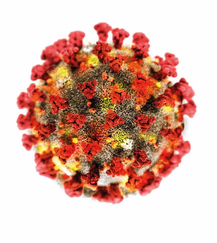
CONTENT

                                      PAGE                                           PAGE                                                  PAGE

                                      18                                            24                                                     28

OPTO-SEMICONDUCTOR PRODUCTS                             ELECTRON TUBE PRODUCTS                        Systems Products

High-sensitivity, High-speed                            Next-generation Ion Detector                  Suitable for In-line
Response Infrared Detector with                         Ideal for Miniature Portable                  Non-destructive
Sensitivity up to 14 μm Band                            Mass Spectrometers                            Inspection

     Cover Story                                                         	OPTO-SEMICONDUCTOR PRODUCTS
3    Photonics and the Fight Against Covid-19                            18   Type II Superlattice Infrared Detector P15409-901
                                                                         19   InAsSb Photovoltaic Detector P13243 Series
                                                                         20   InAsSb Photovoltaic Detector P15742-016DS/-046DS
     Company News                                                        21   MEMS Mirror S13989-01H
4    Ambient Light Sensor Calibration with Tunable Light Sources         22   InGaAs Linear Image Sensor G14714-1024DK
                                                                         23   CCD Area Image Sensor S10420-1106NU-01/-1106NW-01

	R&D Interview
6	“Triode MCP Assembly” Overturns the Accepted View of What             	ELECTRON TUBE PRODUCTS
   a Microchannel Plate (MCP) Can Do!                                    24   MCP Assembly F14844
                                                                         25   Micro PMT R12900U/-01
                                                                         26   Photosensor Module H14601 Series
     Application Report                                                  27   Photon Counting Head H14870
11	SiPM Technology Increases the Safety of Charged Particle Therapy
    through Improved Beam Range Verification
                                                                              SYSTEMS PRODUCTS
                                                                         28   InGaAs Line Scan Camera C15333-10E
	in Focus
14	Significantly Increased S/N in the Weak Light Region from a Unique
    Viewpoint                                                            	LASER PRODUCTS
16	Compound Opto-semiconductor that Can Detect up to 14.5 μm            29   LD Irradiation Light Source L13920-711 SPOLD
	World’s First Mass Production without Using Substances Restricted by
    the RoHS Directive
                                                                              Company News
                                                                         30   Empowering Breakthroughs with Light at Photonics West 2020
                                                                         31   Hamamatsu Photonics K.K. Sales Offices

                          Hamamatsu News –
                          now also online:
                          www.hamamatsu-news.com

2   News 2020 Vol. 1
Cover Story
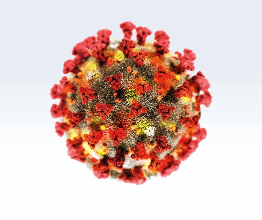
Photonics and the Fight Against Covid-19
Techniques such as PCR and medical imaging are vital in the fight against the coronavirus, which rely on
the continued supply of components by manufacturers such as Hamamatsu Photonics
The novel coronavirus (Sars-Cov-2) continues to spread across the quantity of the genetic material from the smear must be multiplied
world, impacting everything from daily life to the global economy. In in order for there to be sufficient material to determine whether the
these challenging times, the healthcare sector plays a particularly pathogen is present or not. For this purpose, so-called thermocyclers
important role. In addition to protective clothing, respiratory masks are used, which initiate the polymerase chain reaction. In 30 to 50
and respirators, the ability to test rapidly and accurately is vital. cycles, the DNA is amplified exponentially. If the pathogen is present
However, rapid testing demands the availability of various laboratory in the sample, its genetic material will amplify and will be detected.
analysers. Meeting the demand for analytical instruments requires If there is no genome of the pathogen, it will not go through the
that manufacturers continue production, to ensure the continuous multiplication process and therefore not be detected. Using a fluo
supply of critical components across the world. Hamamatsu Photonics rescence dye, the amplification of the pathogen genome can be
is part of the supply chain for products and devices used in the fight monitored in real time. This is called real-time PCR. It usually takes
against the virus. Our products are integrated into many laboratory several days before the patient receives the test result. To send the
analysers and we also work closely with point of care diagnostic sample to the laboratory takes the longest time, the test itself takes
manufacturers to develop new instrumentation for rapid testing. up to five hours.
But never forget: The safety and well-being of our employees is our Hamamatsu Photonics has decades of expertise in the development
top priority. We are monitoring the guidance of the World Health and manufacture of optical technologies. Several manufacturers of
Organisation and other public health bodies closely, and are taking laboratory devices choose Hamamatsu Photonics for products such
appropriate measures to provide our employees with a safe and as photomultiplier tubes (PMTs), photodiodes and cameras that
healthy working environment. allow the optical detection of the target DNA sequence. We are proud
to supply our products to manufacturers of laboratory analysers all
How to fight the virus? over the world that are contributing to fighting the virus.
Researchers around the globe are striving to develop an effective vac
cine against Sars-Cov-2, but this still requires time. To combat the Medical imaging as a further diagnostic tool
further spread of the coronavirus efficiently, immediate detection of the Severe cases of Covid-19 are associated with pneumonia, which
virus is of crucial importance. The aim is to reduce the chain of infec can lead to changes in lung tissue. As a further diagnostic tool of
tion and thus the infection rate. But to identify who is and who is not coronavirus, medical imaging techniques such as computed tomo
infected requires that as many tests as possible are performed. Tedros graphy (CT) and conventional radiography of the thorax are used.
Adhanom Ghebreyesus, head of the World Health Organisation (WHO), Changes of lung tissue are visible in the images obtained through
famously said during a press conference in March: ‘Test, test, test’. these methods. In some cases, the pneumonia associated changes
of lung tissue are already visible despite the test results of PCR
Rapid tests and test analysers being negative. With computed tomography or thorax x-rays, the
To test thousands of people, thousands of rapid tests are required, severity of the disease can be assessed and the clinical indication in
which in turn calls for great numbers of analytical devices for their severe cases monitored.
evaluation. One common analysis method of these devices is the
polymerase chain reaction (PCR). This method is widely used in Compared to PCR, an advantage of medical imaging is that the
molecular biology to amplify the patient’s DNA. results are available immediately. On the other hand, ionising radia
tion is used in CT and X-Ray, so the health benefit for the patient
How does the PCR test work? must outweigh the radiation risk. Hamamatsu Photonics’ contri
First, a smear is taken from the patient’s mouth, nose or throat. This bution in the field of x-ray detection is apparent by a portfolio of
sample is then sent to a laboratory. Each virus can be identified by a suitable x-ray detectors, which it supplies to numerous medical
specific characteristic sequence of its genetic material. However, the equipment manufacturers around the globe.
News 2020 Vol. 1 3
Company News
Ambient Light Sensor Calibration
with Tunable Light Sources
High resolution, high brightness light sources drive profitability in manufacturing
of spectral sensors
As worldwide production of smartphones now exceeds 1.5 billion units per year, premium brands
focus on advancing core functionality to win market share. Ambient light sensors play a key role
in display quality, camera performance, and battery life.
Ambient light sensor calibration
TLS-EQ-77-S ation
f illumin
Entrance slit Area o
EQ-77 Reference
Exit slit Fiber coupled output
Homogenizer
LDLS
Narrow slit
Monochromator Device
More light Under Figure 1: A tunable broadband
Test (D
350 nm –1100 nm UTs) source is used to calibrate
50 mm ambient light sensors.
× 50 m
Xenon Arc m
Narrow slit
Less light
Contribution of ambient sensors to smartphone performance Another important function of ambient light sensors in smartphones
Did you know that the backlight of an LCD display accounts for is white color balance for the display and onboard camera. The smart
approximately 40 % of the overall power consumption of a mobile phone relies on a sensor to correct the white balance, ensuring great
device? There are typically at least two ambient light sensors at images regardless of lighting conditions.
work to extend the battery life of a device by adjusting the display
brightness. Ambient light sensor calibration procedure
The calibration process of high-quality sensors requires illumination
Ambient light sensors, also referred to as color or spectral sensors, with narrow bands of monochromatic light that match the spectral
are simple, low-cost components that have a disproportionately range of the sensors.
large impact on the performance of high-end smartphones.
The sensors are comprised of a small number of photodiodes (3-12)
These sensors are responsible for turning off the display when a with optical coatings that each transmit a different wavelength band
user raises their device to their ear for a call and are used to control of light. The response of each sensor is compared to a reference
the brightness of the smartphone display to optimize the user’s measurement from a spectrometer to evaluate unit-to-unit variation.
experience based on the level of ambient light present. An example calibration setup, featuring the TLS-EQ-77-S Laser-Driven
Tunable Light Source (LDTLS™), is shown in figure 1.
4 News 2020 Vol. 1
High resolution source increases process throughput Read more by visiting
The high spectral radiance of Energetiq’s Laser-Driven Light Source, www.energetiq.com/sensorcalibration
around which the LDTLS product was designed, enables lots of light
to be coupled through a narrow monochromator slit. This provides
a unique combination of narrow-bandwidth and high in-band light Read more
flux. For accurate calibration, the bandwidth of light illuminating the For a more in-depth explanation, please read our app note titled
sensors must be narrow enough to provide the required spectral “Ambient Light Sensor Calibration with Tunable Light Sources”.
resolution.
Additional benefits of LDTLS
While the bandwidth of the monochromatic light source is a critical The high light throughput of the LDTLS is not the only benefit for
parameter for the accuracy of the calibration, it is the in-band light ambient light sensor calibration. The table below highlights several
flux that drives process efficiency, throughput, and profitability. additional benefits.
Laser-Driven Light Source/LDTLS features Benefits
High radiance High in-band light flux enables high process throughput
High spatial stability of plasma Consistent output for accurate measurements
Long-term light flux stability Consistent output for accurate measurements
Convenient fiber-coupled output Ease of integration
Infrequent maintenance 9000 hours between bulb replacements (4× longer than xenon bulbs)
News 2020 Vol. 1 5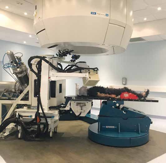
R&D Interview
“Triode MCP Assembly”
Overturns the Accepted View
of What a Microchannel Plate
(MCP) Can Do!
Making mass spectrometry a handy and easy-to-use
tool by approaching issues from a different angle!
Ion detector with high gain and stable operation
even in low vacuum environments!
A completely new and innovative device for ion detection We talked to two people involved in developing and
marketing this new MCP assembly. Let’s hear what
has been developed for use in mass spectrometers that
they have to say.
are commonly used to identify substances. It is an MCP
assembly designed with a unique triode structure and it
overturns the generally accepted view “an MCP cannot
be used at low vacuum levels.” Using a detector that
operates at low vacuum levels, it will eliminate the need
for preparing large vacuum pumps for mass spectro
meters allowing downsizing and cost reduction of the
equipment. As just one of the promising applications,
this new MCP assembly is already getting attention as
a portable explosive trace detector for airport security.
(Left) Masahiro Hayashi
Manuf. #5, Electron Tube Division
(Right) Joji Sakakiyama
Business Planning Management
Business Headquarters
6 News 2020 Vol. 1
The MCP then started to be used in mass spectrometry, right?
“An MCP cannot be used at low vacuum levels.”
This is a generally accepted view that has proven Hayashi: Yes, the MCP is known to be sensitive not only to light, but
to be a barrier until now. also to ions. Moreover, since the sensitive area of the MCP can be
enlarged, it has started to be used as an ion detector for time-of-
Firstly, let me ask both of you “What exactly is mass spectrometry?” flight (TOF) mass spectrometry.
Sakakiyama: Mass spectrometry is an analytical technique used Sakakiyama: However, the current theory is that the MCP is unus
to identify and quantify a substance by ionizing the atoms and able at vacuum levels lower than 10-4 Pascals. Since atmospheric
molecules of the substance, measuring the mass-to-charge ratio pressure is 105 Pascals, this means the MCP could only be used at
and the number of ions. high vacuum levels, where the number of molecules and atoms con
tained in the atmospheric air are reduced to less than one billionth.
Hayashi: What makes mass spectrometry special is its capability
to detect even trace amounts of a substance. For example, let us Is this generally believed to be true?
suppose the Tokyo Dome (baseball stadium) is filled with water and
a tiny amount of salt on the tip of a toothpick is dissolved in that Sakakiyama: Yes, it is. When our customers use a conventional
water. Mass spectrometry has the extremely high sensitivity needed MCP, we still ask them to use it at vacuum levels higher than 10-4
to detect the salt within all that water. Pascals. Meanwhile, for many years, we have had customers saying:
“I really wish I could use an MCP at lower vacuum levels.”
What are the features of the triode MCP assembly you have newly
developed for mass spectrometry? Why do the customers want to use the MCP at lower vacuum levels?
Sakakiyama: A typical MCP consists of a multitude of micro glass Hayashi: To increase the vacuum levels, the air in the equipment
capillaries fused together and sliced into a thin plate less than 1 mm must be sufficiently evacuated. This usually takes a long time and
thick (see figure 1). When electrons pass through each capillary, or requires a large vacuum pump. When using a typical MCP, a high
channel, they are multiplied by secondary emission. voltage of 1 kV is usually applied across a glass plate less than 1 mm
thick. If the vacuum level is not high enough, the residual gases will
Figure 1: Structure of a typical MCP cause electrical discharge leading to malfunctions.
Sakakiyama: So, for these customers who wanted an MCP detector
that operates at lower vacuum levels, our new MCP will make their
lives easier.
What do you mean by “making it easier”?
Channel Output side
Wall Electrode Sakakiyama: For example, it will shorten the vacuum evacuation
Incident time required for the equipment to be operational.
Electron Output
Electrons
Input side Strip
Electrode Current Hayashi: The MCP assembly we have developed is intended for use
Vd in compact desktop mass spectrometers, which usually use a small
vacuum pump. This means the vacuum level that can be obtained
is relatively low.
Hayashi: Our Company developed MCPs about 40 years ago. At that
time the MCP had been mainly used for night-vision goggles, that Sakakiyama: Ion detectors have been the bottleneck in developing
enabled viewing of clear images even in darkness. In night-vision a desktop mass spectrometer with satisfactory performance, as they
goggles, faint light is converted into electrons at the photocathode were unusable at low vacuum levels. There were market needs for
and the electrons multiplied in individual MCP channels, which are such a compact, portable and low cost mass spectrometer and our
then reconverted into light. new triode MCP assembly makes this now a reality.
News 2020 Vol. 1 7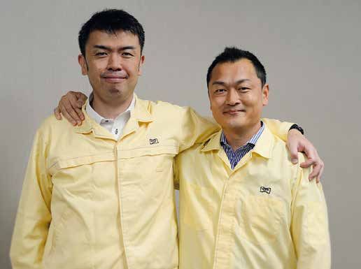
R&D Interview
the beginning of this interview, a great feature of mass spectrometry
Our triode MCP assembly is a breakthrough that
is that it can identify trace substances. The higher the gain of the
delivers high gain (multiplication factor) detector, the more accurate and quicker the measurement will be,
even at low vacuum levels. even when the amount of ions is small. This also increases the
throughput or processing speed.
Are your competitors taking the same approach?
Sakakiyama: Since our newly developed triode MCP assembly can
Sakakiyama: On our competitor’s websites, we see ion detectors be used at low vacuum levels, it will help reduce the size and cost of
with low vacuum levels, but they use a different method from ours. mass spectrometers, making them more portable. What’s more, the
high gain operation will sharply boost the processing speed.
How does your triode MCP assembly differ from competitors’
products in terms of performance?
We changed our approach to “controlling”
Hayashi: Our triode MCP assembly can be used at vacuum levels
the generated ions rather than “suppressing”
one to two orders of magnitude lower than our competitors. Our ion generation.
customers, who have tested our new product in their own equipment,
have verified this. Therefore, your triode MCP assembly has solved a big problem
posed by conventional mass spectrometry. How did you succeed
Sakakiyama: As the operating vacuum level of the detector in using it at low vacuum levels without lowering the gain?
decreases, the required capacity of the vacuum pump also
decreases. This is very important because the size and cost of Hayashi: As shown in figure 3, an ordinary MCP assembly has
mass spectrometers is dependent upon the vacuum pump capacity. a biplanar structure consisting of a two-stage MCP and a signal
Another feature of our triode MCP assembly is that it still maintains readout electrode called the anode. When ions enter the MCP they
high gain (multiplication factor) even when used at low vacuum are converted to electrons, which are multiplied and finally collected
levels. by the anode as an output signal. When the vacuum level is low,
residual gas molecules and atoms remaining in the vacuum system
Hayashi: Yes, it exhibits a high gain of 106 to 107, even in operation react with the electrons from the MCP that causes the generation of
at low vacuum levels. In contrast, rival products can only achieve positive residual gas ions.
lower gain and still at higher vacuum levels. (Figure 2).
So, those generated ions are not needed?
What are the benefits of using a detector with high gain?
Hayashi: That’s right. When residual gas ions are generated, they
Hayashi: The gain of the detector is an important factor that affects move back toward the MCP via an electric field, which is the
the analytical sensitivity of mass spectrometers. As we mentioned at opposite direction of electrons moving to the anode. This is called
Figure 2: Vacuum level and gain Figure 3: Biplanar structure and ion feedback mechanism
Atmospheric High vacuum 1. Electrons move from 2. Residual gas ions 3. Positively-charged
environment environment MCP to anode are generated by residual gas ions
Vacuum (Pa) 10 5 101 1 10 -1 10 -2 10 -3 10 -4 reaction of electrons move back to MCP
and residual gases causing noise
MCP -2100 V Residual
MCP
MCP -2100
-2100VV Residual
gas ions
Residual
Gain 106~107 103~105 106~107
-100 V gas
gasions
ions
-100
-100VV
Residual
Residual
gas
Residual
Competitor Our Electron (-) gas
gas Electron (-)
Electron Anode:
Device Triode type MCP assembly product standard Electron(-)(-) Anode:
Ground
Electron
Electron(-)(-)
MCP Anode:
Ground
potential
Ground
potential
potential
8 News 2020 Vol. 1
MCP -2100 V Residual MCP -2100 V
MCP -2100 V Residual
gas ion MCP -2100 V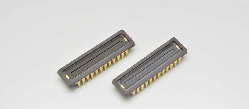
“ion feedback” (in figure 3). When ion feedback occurs, the residual
gas ions collide with the channel walls of the MCP and cause the
emission of electrons. These electrons are then multiplied in the
MCP channel walls generating noise signals. If these noise signals
increase, they will disturb and degrade the high sensitivity and
accuracy of the measurements required for mass spectrometry.
Sakakiyama: For this reason, most users have until now believed
“MCPs cannot be used at low vacuum levels.”
Therefore, your new triode MCP assembly
has “broken the mold”?
Sakakiyama: Yes, in contrast to the
biplanar structure which comprises of
two electrodes, MCP and anode; the
Triode structure is also
triode MCP assembly has three electrodes,
MCP, mesh anode and dynode. We coined
a space-saver.
the name “triode” from ‘tri’ meaning three
and ‘electrode’. That was a terrific idea, but where did the idea
of the triode structure come from?
Hayashi: In the triode MCP assembly as shown in figure 4,
the MCP input side is at the same potential as the dynode. This Hayashi: A triode structure had already been employed in vacuum
means that if residual gas ions are generated, they are trapped by tube transistors. Inserting a mesh or grid as the third electrode is
the dynode while passing through the mesh anode. Meanwhile the a well-known technique. About 10 years ago, our senior engineers
output signal is detected by a mesh anode placed between the MCP had already applied the triode structure to an MCP to enhance the
and the dynode. During the initial stages, we tried hard to suppress signal output speed.
the generation of ions caused by the residual gases reacting with
electrons, but the lower the vacuum level, the greater the number Let us take a look at the actual triode MCP assembly.
of ions generated. We eventually gave up and had to admit that it It is smaller than I thought!
was impossible to suppress the generation of ions. We thought it
would be better to try to control the generated ions rather than to Sakakiyama: This product has an effective diameter of 14.5 mm.
suppress the generation of ions. We finally found a solution utilizing Previously made samples include those with a smaller effective
MCP
MCPMCP -2100-2100
V VV
-2100 Residual
Residual
Residual
the potential gradient in the triode
gasMCP assembly.
gasions
gas
ions ions diameter of 7 mm.
-100
V VV
-100-100
Residual
Residual
Residual
Figure 4: Triode
gas structure
gas
gas
Hayashi: Our MCP is a very small device. Most competitors’ products
Electron
Electron (-) (-)(-)
Electron
Anode:
Anode:
Anode:
Electron
Electron (-) (-)(-)
Electron are relatively large compared to the MCP and their detectors are
1. Electrons move from 2. Residual gas ions 3. Residual gas ions are
Ground
Ground
Ground even larger after assembly. In contrast, the MCP itself is a thin plate
MCP to mesh anode
potential
potential
potential are generated by trapped by dynode at
reaction of electrons the same potential as of around 0.5 mm thick and even when two MCPs are stacked, the
and residual gases MCP-in! total thickness is only 1 mm. In addition, the distance from the MCP to
the mesh anode is at the millimeter scale. Therefore, the overall size
MCP
MCPMCP -2100
-2100 V VV
-2100 Residual
Residual
Residual MCP
MCPMCP -2100
-2100 V VV
-2100 of the triode assembly, complete with the electrodes, is a thickness
gasion
gas gas
ion ion
-100
V VV
-100-100 -100
V VV
-100-100 of around 7 mm. After taking the space-saving benefits into account,
Electron
Electron (-) (-)(-)
Electron I believe the triode structure is the ideal approach. Our new triode
Mesh
MeshMesh Mesh
MeshMesh
(Anode:
(Anode:
(Anode: (Anode:
(Anode:
(Anode: MCP assembly delivers a space-saving package, high gain and
Dynode
Dynode
Dynode
-2100 -2100
V VV
-2100
Ground
Ground
Ground
Dynode
Dynode
Dynode -2100
-2100 V VV
-2100
Ground
Ground
Ground stable operation at low vacuum levels. I do not think there are any
potential)
potential)
potential) potential)
potential)
potential)
other techniques that can simultaneously deliver all these features.
News 2020 Vol. 1 9
R&D Interview
Hayashi: Other potential applications include inspecting for residual
pesticides in agricultural products, animal and plant quarantine
stations and in healthcare, checking for health conditions from the
exhalation of human breath. The equipment becomes affordable,
it has the potential for use in point-of-care-testing for the early
detection of disease. Family health checks could be made at home
and the data sent to the hospital. There are various technical issues
to be addressed, for example, how to operate it at even lower
vacuum levels and to further reduce the size so that the equipment
is more portable and easy to carry.
Sakakiyama: As the long-accepted view is “an MCP cannot be
used at low vacuum levels” even when we emphasized this to our
customers, they did not immediately believe it. However, when our
customers tested our new triode MCP assembly they discovered its
incredible performance. Therefore, we are eager for our customers to
Try its performance, it goes beyond and
evaluate our product and see the high performance and advantages
breaks boundaries! for themselves.
How are sales going at present?
Sakakiyama: We first introduced this new triode MCP assembly Application example of a triode MCP assembly
at the ASMS (American Society for Mass Spectrometry) annual Ion mobility mass spectrometry has been the mainstream for
conference, the world’s largest conference on Mass Spectrometry. explosive trace detectors used at airport security. However, it
Using connections established at that conference our sales pro suffers from false detection errors and only detects a limited
motion activities are currently for customers in the United States number of compound types. Equipment using our triode MCP
and European countries. is the first mass spectrometer Trace Detector which offers the
benefits of both reducing false detection errors and boosting
Hayashi: The greatest feature of the triode MCP assembly is that it processing speed.
can be used at low vacuum levels and is ideal for use in compact
desktop mass spectrometers. So the main market is industries
that manufacture small, compact mass spectrometers, so called
‘miniature MS’. Our triode MCP assembly is also suitable for large-
scale mass spectrometers however MCP assemblies with higher
specifications are normally used, typically with higher gain and
speed. This is due to the high vacuum conditions needed by the
detector in such large-scale mass spectrometers.
Tell me about the future prospects for this triode MCP.
Sakakiyama: Some customers have already decided to use our new
triode MCP assembly for Mass Spectrometry based explosive trace de
tectors. We expect it to deliver a much greater performance compared
to current technology employed by the homeland security market.
For further information see page 24
10 News 2020 Vol. 1Application Report
SiPM Technology Increases the Safety of Charged Particle
Therapy through Improved Beam Range Verification
Abstract
In charged particle therapy, it is of great importance to monitor the range of the ion beam within patients to guarantee
the safety and effectiveness of the treatment. An innovative bi-modal system based on Hamamatsu MPPC Silicon
Photo Multipliers (SiPM) technology was developed to monitor range variations and check compliance with the
planned treatment. The system is based on the detection of the secondary radiation emitted by nuclear interactions of
the beam with the patient’s body. The system, named INSIDE, is the result of a collaboration between the Universities
of Pisa, Sapienza Roma, Torino, Bari Polytechnic, the National Institute for Nuclear Physics (INFN), Historical Museum
of Physics and the Enrico Fermi Study and Research Center (CREF), the Center of Oncological Hadrontherapy (CNAO).
The INSIDE system is now undergoing clinical trials at CNAO.
Introduction complementary information provided by two different detection
Charged particle therapy (CPT), or hadrontherapy, is an advanced systems, a PET scanner and an IVI system called a dose profiler (DP).
radiotherapy technique that uses accelerated proton or carbon ion The INSIDE detector technology is based on inorganic scintillating
beams to treat solid tumors with extreme precision. Charged particles crystals (for the PET detector) and scintillating fibers (for the DP
release most of their energy at the end of their path (in the region detector), with read-outs based on Hamamatsu MPPC SiPMs.
called the Bragg peak) which is dependent on the energy of the
particles. This property allows healthcare staff to target cancer cells SiPMs have many properties that make them ideally suited for such
very specifically, significantly reducing the dose to the surrounding a demanding application. Because of their small size and flexibility
healthy tissue. To verify that the treatment has been delivered when designing the sensor, it is straightforward to build a detector
according to plan, instruments indirectly measure the position of the configuration optimized for the constraints on the patient set-up
Bragg peak in a process called “beam range verification”. and on that beam. The pixel dimension can be adjusted during
manufacture to set the desired spatial resolution of ~2 mm. SiPMs
The most widely used approach for proton CPT is Positron Emission have a fast response time which, when coupled with the appropriate
Tomography (PET). This technique measures the activity of the posi electronics read-out scheme, means that data can be processed at
tron emitting radionuclides produced by the nuclear interactions the rates on the order of hundreds of kHz. Finally, SiPM technology
between the beam and the traversed tissue. In carbon ion therapy, is fully compatible with the safety requirements of a treatment room,
Interaction Vertex Imaging (IVI) is a promising technique but it is as no high voltages are needed.
so far clinically unexplored. IVI exploits the production of secondary
charged particles upon the nuclear fragmentation of carbon ions in The first phase of the INSIDE project, which focused on the develop
tissue. The charged fragments, emitted at almost the same velocity of ment of the two detectors, was carried out between 2013 and 2016.
the primary ion, exit the patient and pass through a tracking system Patient experimentation and clinical studies represent the second
that reconstructs their emission point and provides information of phase of the INSIDE project. These took place in one of the three
the primary ion beam’s range. CNAO treatment rooms where the two detectors have been installed
on a movable cart that can be positioned next to the patient bed
INSIDE (INnovative SolutIons for Dosimetry in hadronthErapy) [1] without interfering with the treatment beam (figure 1). The third
is an innovative beam range verification system based on the phase of the project is full clinical trials.
News 2020 Vol. 1 11Detector
The INSIDE PET detector is made of two planar heads placed 60 cm
apart, above and below the patient bed with the treatment room
isocenter in the center of them (figure 1). Each head (figure 2)
is composed of a 2 × 5 array of detection modules developed by
DP
Hamamatsu (model S12642-1616-3577(X)). The heads are enclosed
in a 0.5 mm thick aluminum case and have a total area of 112 mm
(transaxial) × 264 mm (axial, along the beam direction). Each of the de
tector modules in the heads have an array of 16 × 16, 3 × 3 × 20 mm
lutetium fine silicate (LFS) crystals. The LFS array is optically coupled
to a matching array of MPPC SiPMs with a microcell size of 50 µm.
PET A rigid-flex electronics board for connecting to the front-end elec
tronics makes up the final element of the detector modules. Each
module has an area of 51.2 × 51.2 mm.
The INSIDE DP detector (figure 3) is made of 8 scintillating fiber stereo-
Figure 1: The INSIDE system in the CNAO treatment room. layers, fixed in place with an aluminum frame, that allow reconstruction
of the track to extrapolate the emission points of protons exiting the
(a) patient. The DP planes are made of 500 × 500 µm multi-cladding
scintillating fibers, which are measured with Hamamatsu MPPC
SiPMs (model S12571-050P) with a 1 mm2 active area. Each SiPM
is coupled to two fibers. 384 fibers make a plane whose active area
is 19.2 × 19.2 cm. The DP is placed 50 cm from the treatment room
(i) (ii) (iii) isocenter and is tilted at 60 degrees with respect to the beam direc
tion (figure 1). The inter-plane distance is 2 cm.
(b) (c)
All detector channels for both systems are processed by custom
integrated front-end electronics and highly parallelized data acqui
sition systems based on field programmable gate arrays (FPGAs).
Two independent cooling systems stabilize the detectors temperature
Figure 2: by means of circulating refrigerated water.
(a) (i) LSF crystal array, (ii) SiPM array and (iii) hybrid rigid-flex circuit for
connection to front-end electronics.
(b) 10 detection modules assembled in a 2 × 5 array (PET head). Performance
(c) Aluminum box hosting the PET head with details of the modules placement The INSIDE system has been installed and tested at CNAO with their
(on the backside), front-end boards on the sides and cooling pipes.
clinical beams. Its performance was assessed in several measure
ment campaigns.
(a) b)
Following the pulsed time structure of the CNAO beam, the PET
system was operated both during the actual delivery of the beam spill
(single event count rate of 20 MHz) and during the interval between
two consecutive spills. The coincidence time resolution (CTR) is
450 ps and the coincidences are calculated on the fly after applying
a time window of 2 ns. The PET image reconstruction was done
with a fast MLEM iterative algorithm whose output is provided with
a small delay of a few seconds with respect to the actual beam spill.
Figure 3:
(a) Picture of the DP layers showing the fibers fixed to the aluminum frame. This is a short enough time to allow treatment interruption in case
(b) Picture of a SiPMs board. of a detected error in the beam range. The INSIDE PET detector has
12 News 2020 Vol. 1Application Report
been successfully used to monitor a patient with a lacrimal gland Conclusions
tumor in two consecutive treatment sessions [2]. Presented here is the first bi-modal system for treatment range
monitoring in charged particle therapy. INSIDE is able to simulta
The DP has a detection efficiency of ~ 90 % and is therefore capable neous ly acquire and process annihilation photons and charged
of performing fragment tracking at up to 100 kHz [3]. The fragment nuclear fragments thus providing a robust tool for bream range
tracking is performed using a tracking algorithm based on the Hough verification.
transform. The 3D coordinates of the fragment production point were
calculated using the point of closest approach (PCA) of the track to the The first clinical results suggest INSIDE’s suitability for acquiring
incoming beam direction. The backtracking resolution is of 7 mm at data within a treatment fractions with both modalities. The stability
50 cm from the isocenter. and reproducibility of the system also allows us to compare data
from different fractions, thus providing longitudinal beam monitoring
A clinical trial totaling 20 patients (10 with proton beams and 10 with of the entire treatment cycle.
carbon ion beams) with selected head and neck or brain pathologies
has been carried out to test the effectiveness and potential clinical Hamamatsu MPPC SiPM technology proved to be instrumental to
benefits of an on-line treatment verification device [4]. First results the successful integration of the INSIDE system in a clinical setting
are shown in figure 4. and makes it the ideal solution for multi-modal on-line beam range
verification in charged particle therapy.
(a) (b)
Acknowledgements
The authors would like to give thanks to the following organizations
that made this work possible. The Italian Ministry of University and
Research for designating the work on a project of relevant national
interest. The University of Pisa for financing and acting as a coor
dinator. The University of Sapienza Roma, the National Institute of
Nuclear Physics and the Historical Museum of Physics and the Enrico
Fermi Study and Research Center for financing and collaboration. Our
Figure 4: collaborators at Bari Polytechnic and University of Torino for study
(a) PET image superimposed to the CT of a patient treated with proton beams and research. Finally the National Center of Oncological Hadron
(coronal view).
(b) PCA map superimposed to the CT of a patient treated with carbon ions therapy (CNAO), the largest Italian facility and one of the few dual ion
(sagittal view). CPT facilities in the world, for their financing and support with trials.
References Authors
[1] Bisogni, M.G., Attili, A., Battistoni, G., Belcari, N., Camarlinghi, N., Cerello, P., Coli, S., M. G. Bisogni 1, 2, G. Battistoni 3, N. Belcari 1, 2, P. Cerello 4, M. Ciocca 5, M. De Simoni 6, 7,
Del Guerra, A., Ferrari, A., Ferrero, V., Fiorina, E., Giraudo, G., Kostara, E., Morrocchi, M. Donetti 5, Y. Dong 3, 8, A. Embriaco 9, V. Ferrero 4, E. Fiorina 4, 5, M. Fischetti 7, 10, G. Giraudo 4,
M., Pennazio, F., Peroni, C., Piliero, M.A., Pirrone, G., Rivetti, A., Rolo, M.D., Rosso, V., A. Kraan 2, F. Laurina 1, 2, C. Luongo 15, 2, M. Magi 10, E. Malekzadeh 11, C. Mancini-Terracciano 6, 7,
Sala, P., Sportelli, G., Wheadon, R. M. Marafini 7, 12, I. Mattei 3, E. Mazzoni 1, 2, R. Mirabelli 6, 7, 12, M. Morrocchi 1, 2, S. Muraro 3,
INSIDE in-beam positron emission tomography system for particle range monitoring in A. Patera 4, V. Patera 7, 10, 12, F. Pennazio 4, A. Retico 2, A. Rivetti 4, M. D. Rolo 4, V. Rosso 1, 2,
hadrontherapy | (2017) Journal of Medical Imaging, 4 (1), art. no. 011005 A. Sarti 7, 10, 12, A. Schiavi 7, 10, A. Sciubba 10, 12, 13, E. Solfaroli Camillocci 6, 7, 14, G. Sportelli 1, 2,
[2] Ferrero, V., Fiorina, E., Morrocchi, M., Pennazio, F., Baroni, G., Battistoni, G., Belcari, S. Tampellini 5, M. Toppi 10, 13, G. Traini 7, 12, S. M. Valle 3, F. Valvo 5, V. Vitolo 5, R. Wheadon 4
N., Camarlinghi, N., Ciocca, M., Del Guerra, A., Donetti, M., Giordanengo, S., Giraudo,
G., Patera, V., Peroni, C., Rivetti, A., Rolo, M.D.D.R., Rossi, S., Rosso, V., Sportelli, G., (1) Dipartimento di Fisica “E. Fermi”, Università di Pisa, Italy (2) INFN Sezione di Pisa, Italy,
Tampellini, S., Valvo, F., Wheadon, R., Cerello, P., Bisogni, M.G. (3) INFN Sezione di Milano, Italy (4) INFN Sezione di Torino, Italy, (5) Centro Nazionale di
Online proton therapy monitoring: Clinical test of a Silicon-photodetector-based Adroterapia Oncologica (CNAO), Pavia, Italy, (6) Dipartimento di Fisica, “Sapienza” Università
in-beam PET | (2018) Scientific Reports, 8 (1), art. no. 4100 di Roma, Italy, (7) INFN Sezione di Roma1, Italy, (8) Dipartimento di Fisica, Università
[3] Traini, G., Mattei, I., Battistoni, G., Bisogni, M.G., De Simoni, M., Dong, Y., Embriaco, A., degli Studi di Milano, Italy, (9) INFN Sezione di Pavia, Pavia, Italy, (10) Dipartimento di
Fischetti, M., Magi, M., Mancini-Terracciano, C., Marafini, M., Mirabelli, R., Muraro, S., Scienze di Base e Applicate per l’Ingegneria (SBAI), “Sapienza” Università di Roma, Italy,
Patera, V., Schiavi, A., Sciubba, A., Solfaroli Camillocci, E., Valle, S.M., Sarti, A. (11) Department of Medical Physics, Tarbiat Modares University, Tehran, Iran, (12) Museo
Review and performance of the Dose Profiler, a particle therapy treatments online Storico della Fisica e Centro Studi e Ricerche Enrico Fermi, Roma, Italy, (13) INFN Sezione
monitor | (2019) Physica Medica, 65, pp. 84-93. dei Laboratori di Frascati, Italy, (14) Scuola di Specializzazione in Fisica Medica, “Sapienza”
[4] ClinicalTrials.gov ID: NCT03662373 Università di Roma, Italy (15) Dipartimento di Chimica, Università’ di Pisa, Italy
News 2020 Vol. 1 13In Focus
ORCA-Fusion C14440-20UP, Digital CMOS Camera for Scientific Measurement
Significantly Increased S/N in the Weak Light Region
from a Unique Viewpoint
New-generation CMOS camera for scientific Achieved 2 × S/N compared to conventional
measurement models by pursuing low-noise
CMOS cameras for scientific measurement (sCMOS cameras) are While live cell imaging technology has been developed, further im
used at the forefront of Life science research, from molecules to provement in the signal-to-noise ratio (S/N) of images has become a
cells, tissues, and individuals. In the past in order to improve the major challenge. In biological observations, the light sensitivity of the
performance of sCMOS cameras, it has been thought that improving camera is closely related to the progress of research. If we can observe
the “Quantum Efficiency” (QE), which converts light into electrons, with less light with less excitation light, we can reduce phototoxicity
is the most appropriate method. Hamamatsu Photonics, however, and fluorescence fading, which makes it possible to observe over
has shown a new path to the evolution of sCMOS cameras with a a longer period of time. There are two main approaches to making
unique approach that focuses on “reducing readout noise.” We will sCMOS cameras more sensitive: improving QE and reducing readout
introduce our new-generation sCMOS cameras, ORCA-Fusion. noise. Up to now, it has generally been considered that improving
QE is the most effective way to achieve high sensitivity. However,
the weaker the light, the greater the effect of noise on the signal-
Contributing to the development of sciences in to-noise ratio. Hamamatsu Photonics has therefore developed a new
various areas through detection technology for dedicated sensor specifically designed for low readout noise and
ultra-weak light areas has succeeded in significantly reducing readout noise while keeping
QE intact by combining its proprietary circuit technology. As a result,
Live cell imaging, which observes the activity of live cells in real the S/N ratio is increased to the highest 2 ×, the image quality is
time, is an essential tool for life science, such as developing new greatly improved by suppressing the variation between pixels, and
pharmaceuticals and conducting genetic researches. To support this the frame rate is improved by shortening the exposure time. By
development, we have been researching fluorescence observation further improving the basic performance of the camera, it can be
methods and cameras for scientific measurement that accurately expected to be applicable for a wider range of applications.
capture a small amount of light. The origin of Hamamatsu Photonics
scientific measurement cameras was in the 1960s, when we re
leased our first Measurement TV camera system.
Above all, sCMOS cameras, which are suitable for imaging in weak
light areas, are ideal for observing living cells due to minimizing light
damage to living organisms and have become indispensable for Mitochondria of HeLa
Cells stained with
research in the life science field. In 2010, we launched the first
fluorescent dyes
generation sCMOS camera, ORCA-Flash 2.8, ahead of the world. (Imaging by
In the weak light area that has been cultivated over many years ORCA-Fusion)
since then, we have developed ORCA-Flash 4.0, the sCMOS camera
that combines sensor and circuitry technologies, and moved to the
second generation. This technology has also contributed greatly to
the development of the Nobel Chemical Prize “Super-Resolution
Microscopy Technology,” which was awarded by Dr. Betzig, Dr. Hell,
and Dr. Moerner et al. in 2014.
14 News 2020 Vol. 1History 2010 2011 2018
Hamamatsu Photonics cameras First-generation Second-generation THIRD-generation
for scientific measurement ORCA-Flash 2.8 ORCA-Flash 4.0 ORCA-Fusion
Number of pixels 2.8 M pixels 1920 (H) × 1440 (V) 4.2 M pixels 2048 (H) × 2048 (V) 5.3 M pixels 2304 (H) × 2304 (V)
Frame rate 45.4 frames per second 100 frames per second 89.1 frames per second
Readout noise 3 electrons rms 1.4 electrons rms 0.7 electrons rms
Main features
Low readout noise 0. 7 electrons rms Acquires highly uniform images
The new approach of “reducing read noise” realizes a readout noise Drastic decrease of pixel-to-pixel variation eliminates the need for
of 0. 7 electrons rms, which is ½ of the conventional one. As a result, image correction, which was previously essential, making it suitable
we have achieved a signal-to-noise ratio of up to 2 ×. for quantitative measurement.
Gen II Cameras with Readout noise distribution (electrons)
cameras improved QE only ORCA-Fusion 10 6
ORCA-Fusion
Number of pixels (pixels)
10 5 Good! Fewer pixels have Gen II sCMOS cameras
Readout Readout Readout
noise noise noise
S/N large readout noise, Bad, there are many pixels
10 4
improvement variation between pixels with large readout noise,
1.4 1.4 0.7 Max. 2 × 10 3 is small. large variation between
pixels.
Electrons Electrons Electrons
10 2
Quantum S/N Quantum Quantum 10 1
efficiency improvements efficiency efficiency
up to 10 0
82 % 1.16 times 95 % 82 % 0 1 2 3 4 5 6 7 8 9 10 11 12 13 14 15 16 17 18 19 20
Readout noise (electrons)
Imaging simulation example: ultra-low light fluorescence Comparison of dark images between ORCA-Fusion and
live cell imaging Gen II sCMOS cameras
Examples of images captured by each camera are shown according ORCA-Fusion Gen II sCMOS cameras
to the number of incident photons.
1.4 2.8 5.6 11.2 22.4 44.8
ORCA-Fusion (Gen III) 2048 × 2048 2048 × 2048
(without correction) pixels pixels (without correction)
100 × 100 pixels 100 × 100 pixels
ORCA Flash 4.0 V3 (Gen II)
2 × faster frame rate in Light Sheet Mode
Equipped with Light Sheet Mode (patented), similar to the previous
QE 95 % sCMOS (Gen II) ORCA-Flash 4.0. It achieves high-speed processing at 100 frames
* The Gen III shows the new sCMOS camera and the Gen II shows the old sCMOS camera. per second, which is 2 × compared to the same vertical pixel count.
Target is With the new approach of reducing readout noise, the potential of sCMOS cameras is once again expanding. The ulti
Multi-Photon mate goal is to realize a camera that can detect multiple photons simultaneously with the accuracy of detecting each
Counting photon. Hamamatsu Photonics is pursuing further reduction of readout noise together with improving QE, which is
a conventional method, to realize the products that meet the needs of a wider range of customers than ever before.
News 2020 Vol. 1 15In Focus
Type II Superlattice Infrared Detector P15409-901
Compound Opto-semiconductor that Can Detect
up to 14.5 μm
World’s First Mass Production without Using Substances
Restricted by the RoHS Directive
Hamamatsu Photonics is actively engaged in environmental con Mid infrared spectrophotometers
servation activities and in the pursuit of environmentally friendly that are required to comply with
manufacturing. We have contributed to the preservation of the RoHS Directives
global environment, the reduction of environmental burden and
have been developing products with the impact on the environment Spectrophotometry is an analysis method in which
always in mind. As a compound opto-semiconductor device capable substances contained in liquids and gases are identified by
of detecting up to 14.5 μm, the world’s first “Type II superlattice using the property that the ratio of light emission and absorption
infrared detector,” was successfully mass produced without using varies depending on the bonding state of molecules and atoms.
substances restricted by the RoHS Directive*1, is one such product
that reflects our efforts. The Fourier transform infrared spectrophotometer (FTIR) is used
in a wide variety of fields such as food, agriculture, and medical
care because it covers a wide range of absorption bands of organic
substances existing near 14 μm.
However, many mid infrared detectors used in FTIR have elements
containing mercury and cadmium, which are regulated by an EU
RoHS Directive, so there was a need to develop an alternative
product. Therefore, we have been developing infrared detectors
that can detect up to the 14 μm band, which was not possible with
conventional InAsSb*2 photovoltaic detectors.
Hamamatsu infrared detector lineup
1011
14 µm band
3 µm band
10 8 µm band
10
5 µm band
D* at λp (cm∙Hz1/2/W)
10 9
P10090 P12691- 10 µm band P15409-901
series 201G
P13243
10 8 series
10 7
P13894
series
10 6
3 5 8 10 14 15
Cutoff wavelength (µm)
16 News 2020 Vol. 1Mass production of Type II superlattice infrared Main features
detectors Hamamatsu’s unique manufacturing technology made mass
production possible
Until now, Hamamatsu has developed and sold InAsSb photovoltaic
detectors that can detect up to 11 μm. Unlike typical opto-semiconductors, the main feature of this product
is the “superlattice” structure in which thin films of InAs and GaSb*3
In the past, Type II superlattice infrared detectors have been con compounds, each with a thickness of several nanometers, are alter
sidered as a way of detecting mid infrared light with a wavelength nately stacked to more than 2000 layers.
longer than 11 μm, but there was a problem in mass production
because it required high manufacturing technology. So, we solved Mass production was achieved by precisely controlling the amount
the manufacturing problems by using the crystal growth technology and timing of stacking InAs and GaSb to the substrate using
of compound opto-semiconductor devices cultivated over many Hamamatsu’s unique com pound semi conductor tech nology and
years and achieved the world’s first mass production of Type II optimizing temperature, pressure, and other conditions to establish
superlattice infrared detectors. a manufacturing method.
Spectral response Structure differences
1000
1011 Elec- Thin films with Elec-
trode a thickness of trode
100Contact layer several nanometers Contact layer
alternately stacked
Light
10 receiving layer Elec- Light receiving layer Elec-
Output (relative value)
1010 trode trode
D* (cm∙Hz1/2/W)
Contact layer Contact layer
1
Substrate Substrate
0.1 Typical compound This product
10 9 opto-semiconductor device
0.01
0.001
Excellent output linearity
10 8
0.01 0.1 1 10 100 1000
1 2 3 4 5 6 7 8 9 10 11 12 13 14 15
Wavelength (µm)
Another main feature of this pro
Incident duct
light levelis(mW)
the output linearity up to
a higher incident light level compared to the MCT*4 and other
conventional detectors. The wide dynamic range can be expected to
increase the precision of analyzers.
More analytical instruments without restricted
substances
Linearity
Infrared wavelengths are not only used in FTIR but also in a wide 1000
11
range of10other applications, such as gas component analysis and
object temperature measurement. Such analytical instruments and 100
measuring instruments may also use detectors containing substances
10
Output (relative value)
restricted10by
10
the RoHS Directive. Replacing those detectors with this
D* (cm∙Hz1/2/W)
product will eliminate the use of restricted substances and achieve 1
higher accuracy.
0.1
10 9
*1 The RoHS Directive is an EU ban on the use of certain hazardous substances in electrical and elec- 0.01
tronic equipment. It prohibits the sale of electrical and electronic equipment that contains more than
a specified concentration
8
of the restricted substances in the EU market. 0.001
*2 InAsSb: In10
(indium), As (arsenic), Sb (antimony) 0.01 0.1 1 10 100 1000
1 2 3 4 5 6 7 8 9 10 11 12 13 14 15
*3 GaSb: Ga (gallium), Sb (antimony) Incident light level (mW)
Wavelength (µm)
*4 MCT (HgCdTe): Hg (mercury), Cd (cadmium), Te (tellurium)
News 2020 Vol. 1 17New OPTO-SEMICONDUCTOR PRODUCTS
Type II Superlattice
Infrared Detector
P15409-901
Specifications Spectral response
Parameter Specification Unit (Typ. Tchip= -196 deg. C.)
Cooling Liquid nitrogen – 10 11
Photosensitive area 0.1 mm
Cutoff wavelength*1 14.5 μm
Peak sensitivity wavelength 5.4 μm
10 10
D* (cm∙Hz1/2/W)
Photosensitivity*2 2.6 A/W
Shunt resistance*3 2.5 kΩ
Terminal capacitance*4 50 pF
Detectivity*5 1.6 × 1010 cm Hz1/2/W
• 10 9
Noise equivalent power*2 5.5 × 10⁻¹² W/Hz1/2
*1 Wavelength at which signal/noise = 1
*2 = p
10 8
*3 VR = 10 mV 1 2 3 4 5 6 7 8 9 10 11 12 13 14 15
*4 VR = 0 V, f = 1 MHz Wavelength (µm)
*5 = p, fc = 1200 Hz, Δf = 1 Hz
High-sensitivity, High-speed Response Infrared Detector
with Sensitivity up to 14 μm Band
The P15409-901 is a Type II superlattice This is a replacement for conventional Features
infrared detector whose sensitivity has products that contain these substances. Metal dewar package (liquid nitrogen
been expanded to the 14 μm band using cooling)
Hamamatsu unique crystal growth techno Differences from the previous product High sensitivity
logy and process technology. This product The cutoff wavelength has been extended High-speed response
is an environmentally friendly infrared to approximately 14 μm (longer than the Excellent linearity
detector and does not use mercury or previous MCT photovoltaic detector).
cadmium, which are substances restricted Applications
by the RoHS Directive. Further, linearity has been improved FTIR
significantly. Gas analysis
Radiation thermometers
18 News 2020 Vol. 1New OPTO-SEMICONDUCTOR PRODUCTS
InAsSb Photovoltaic Detector
P13243 Series
(with Band-pass Filter)
Two-element type Ceramic type Metal type
P13243-015CF P13243-033CF P13243-033MF
P13243-016CF P13243-039CF P13243-039MF
P13243-043CF P13243-043MF
Specifications Spectral response
Center wavelength Spectral response Photosensitivity*1 Detectivity*2 (Typ. Ta = 25 deg. C.)
Type no.
(nm) half width (nm) 10 11 (mA/W) (cm Hz1/2/W)
• 4.0
P13243-033CF/-033MF 3300 160 2.3 5.1 × 10⁸ 3.5 P13243-043MF/-043CF
P13243-039CF/-039MF 3900 90 3 6.5 × 10⁸ P13243-039MF/-039CF
3.0
P13243-043CF/-043MF 4260 140 3.1 6.9 × 10⁸
Photosensitivity (mA/W)
10
10
3300 160 2.3 5.1 × 10⁸ 2.5 P13243-033MF/-033CF
D* (cm∙Hz1/2/W)
P13243-015CF
3900 90 3 6.5 × 10⁸ 2.0
3900 90 3 6.5 × 10⁸
P13243-016CF 1.5
4260 140 10 9 3.1 6.9 × 10⁸
1.0
*1 = CWL (center wavelength),
uniform irradiation on the entire photosensitive area 0.5
*2 = CWL, fc = 1200 Hz, Δf = 1 Hz
10 8 0
1 2 3 4 5 6 7 8 9 10 11 12 13 14 15 2.5 3.0 3.5 4.0 4.5 5.0
Wavelength (µm) Wavelength (µm)
Infrared Detectors with a Band-pass Filter
(3.3/3.9/4.26 μm)
These are InAsSb photovoltaic detectors for conventional products that contain these Applications
that employ a band-pass filter for the win substances. In addition, a two-element type Gas detection (CH4, CO2)
dow. Three types are available with different (P13243-015CF/-016CF), which can detect Flame detection
band-pass filter center wavelengths for two wavelengths, is available.
various applications: 3.3 μm (CH4), 3.9 μm
(reference light), 4.26 μm (CO2). These are Features
environmentally friendly infrared detectors High sensitivity
and do not use lead, mercury, or cadmium, High-speed response: 15 ns
which are substances restricted by the High shunt resistance: 300 kΩ
RoHS Directive. These are replacements Compatible with to lead-free solder reflow
News 2020 Vol. 1 19New OPTO-SEMICONDUCTOR PRODUCTS
InAsSb Photovoltaic Detector
P15742-016DS/-046DS
Specifications
Parameter P15742-016DS P15742-046DS Unit
Cooling Non-cooled –
Element size 0.45 × 0.7 (× 16 ch) 0.2 × 0.7 (× 46 ch) mm
Element pitch 0.5 0.25 mm
Cutoff wavelength 5.3 μm
Peak sensitivity wavelength 3.5 μm
Photosensitivity*1 7.0 14.6 mA/W
Shunt resistance*2 100 60 kΩ
Detectivity*3 1.0 × 109 cm Hz1/2/W
•
*1 = p *2 VR = 10 mV *3 = p, fc = 1200 Hz, Δf = 1 Hz
Photodiode Array with Sensitivity up to the 5 μm Band
for Simple Spectrophotometry
These are 16 ch/46 ch InAsSb photodiode Differences from previous products Features
arrays that can detect up to the 5 μm band. Like the InAsSb photovoltaic detector High sensitivity
Low crosstalk has been achieved by P13243 series, these are an array type 16 ch/46 ch array
adopting a back-illuminated structure. with a 5 μm band cutoff wavelength. Back-illuminated structure: Low crosstalk
The wavelength is longer than that of
the conventional InGaAs photodiode Applications
array G12430-016D/-046D. Radiation thermometers
Infrared spectrometer
20 News 2020 Vol. 1You can also read