Project Call for Participation: PLP Fine Pitch Substrate Inspection/Metrology, Phase 4 - iNEMI
←
→
Page content transcription
If your browser does not render page correctly, please read the page content below

Project Call for Participation:
 PLP Fine Pitch Substrate
 Inspection/Metrology, Phase 4

January 20-21, 2022      Listen to the recorded webinar

Feng Xue, IBM            YouTube: https://youtu.be/N2GLkoOaipw

Joe Zhihua Zou, Intel    Other video: http://thor.inemi.org/
Charles Reynolds, IBM    webdownload/2022/Projects/
                         PLP_fine_pitch_inspect-4_cfp.mp4
iNEMI Project Manager:
Masahiro Tsuriya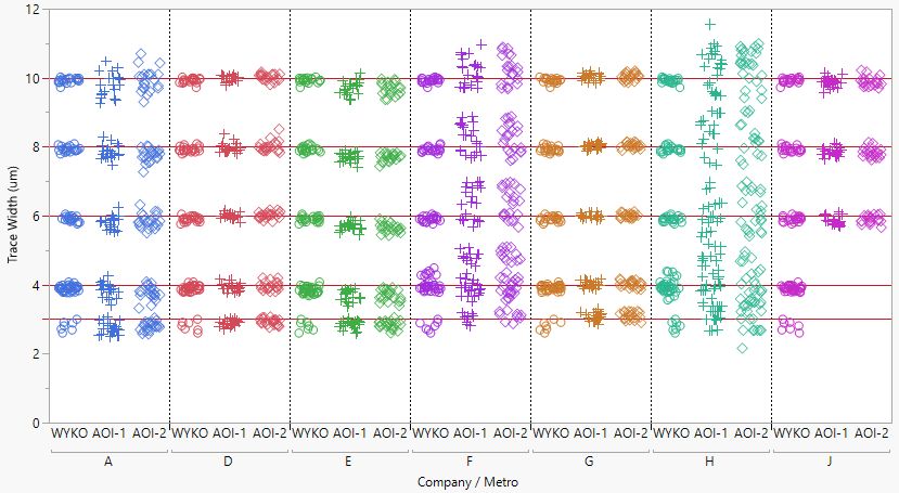
Agenda

         • Introduction of Project Chairs
         • iNEMI Project Development Process
         • Project Briefing
          •   Background
          •   Objectives
          •   Scope
          •   Timeline
          •   Resource
         • How to Join
         • Q&A
                     Note: All phones will be on mute until the end of the presentation
 2
Introduction of Project Chairs

    Feng Xue (IBM)                            Joe Zhihua Zou (Intel)                    Charles Reynolds (IBM)
    Job title: Senior Technical Staff         Job title: Principle Engineer, Ph.D.      Job title: Senior Technical Staff
    Member                                                                              Member
                                              Experience:
    Experience:                               •   19 years experience in                Experience:
    •   17 years experiences in                   semiconductor technology of R&D on    •   More than 30 years experience in
        semiconductor technology, quality         substrate manufacturing, metrology,       packaging design and development
        management and supply chain               inspections and testing, quality      •   Currently focuses on CSP
        operation                                 control, 3D packaging as well as          development
    •   Current role as Chief Architect for       supplier chain management
        Supply Chain Quality System & i4.0    •   Currently program manager as 3D
        Solutions                                 packaging R&D and next generation
    •   Member of IBM Academy of                  metrology on advanced substrates
        Technology

3
iNEMI Project Development Process

                1
                          CONCEPT

                 2        DEFINITION                                              “ Initiative”
                                                                            Open for Industry input
                 3        PLANNING
            ------------------- iNEMI Technical Committee (TC) Approve SoW & PS
                 4        LAUNCH

                 5        EXECUTION                                                “ Project”
                                                                       Limited to committed Members
                 6        CLOSURE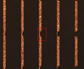
iNEMI Project Management Policy

     • Two governing documents for projects
       • SOW (statement of work): sets out project scope,
         background, purpose, benefits, and outlines required
         resources, materials, processes, project schedule, etc.
       • Project Statement (PS): signed by participating
         companies to secure commitment on resource and time
         contributions.

     • iNEMI Project requires iNEMI membership
       • Signed membership agreement
       • Commitment to follow iNEMI By-laws and IP policy

 5
Project Briefing
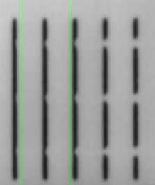
Project Background
 • Heterogeneous SiP packages are popular as an electronic packaging solution. In addition, circuit boards are
   incorporating high-dense circuit patches and layers to support increased signal requirements. This technology
   requires finer circuitry patterns and designs. However, it is difficult to validate and measure the designed line
   width and spaces, and to detect defective features.
 • Measurement capability on fine line (
Key Element for AOI Measurement
 • Optics:                                                                       • Type of Analyses:
   • High Resolution/ Selectable Magnification is needed                         • Inspection: Detection of any variation based on given requirement.
                                                                                    • Comparing against Reference (CAD or Golden Reference Image)
                                                                                    • Comparing against Fixed Values (Absolute Reflection Values)
                                                                                    • Comparing against Neighborhood
                                                                                 • Metrology: Measuring of defined Objects
                                                                                    • Absolute Measuring (Measuring the dimension of a defined Object)
                                                                                    • Overlay Measuring (Position of defined Objects to each other or
                                                                                       Reference Point)
                                                                                 • Post Processing:
                                                                                    • Analyzing data based on given Models (coplanarity for Bumps)
 • Light source:                                                                    • Process Control based on feedback of variations over Lots/Time
    • Adjustable light source / angle / color filter(s) to enhance contrast         • Generating Maps and Reports
 • Alignment:
                                                                                                                            Camera
    • Perform comparison from AOI product image to design requirements
        to validate results and avoid defect false alarms
 • Inspection policy:                                                                                                      Bright Field Illumination

    • Assess different algorithms to fit different materials and design
 • Filter:                                                                                                                    Multiple Resolution

    • In order to separate the defects, auto filtering is needed to categorize
        the defects into predefined groups.
                                                                                                                          Dark Field Illumination
                                                                                                           Wafer
 8
Sample of Phase 3 Results Unit-Top A D E F G H J 10um 8um 6um 4um 3um 9
Sample of Phase 3 Results

 10
Project Objective
Motivation:
◼   With the deployment of finer pitch substrate features in advanced packaging (SiP, 2.5D etc), there is a need
    to identify and characterize the capabilities of inspection technologies that can enable faster process
    development and higher yield in volume production.
◼   Continue from phase 3 to expand the study for 1.5um to 5um designed organic TV.
                                                                                                                   TV design will be changed to meet Phase 4 objective.
Objective:
◼   There are two steps for this project.
◼   Step 1 is to conduct the industry survey to understand what are changed form previous survey results
    conducted in 2016.
◼   Step 2 is to evaluate current inspection & measurement capabilities for fine pitch substrates that will be
    needed over the next 5 years.
        ◼   AOI measurement and inspection studies includes the various defects types and also the narrow
            trace widths.
◼   Assess the AI assisted AOI inspection system and readiness for finer trace patterning.
Strategy/Approach:
◼   Identify the potential fabricator who could make phase 4 test vehicle sample with below 5um line space
    design.
◼   Design and Fabricate Test Vehicle on organic substrate (using Phase 3 TV design as the base reference).
    Design for TV contains trace width nominal of 5um, 3um, 2um and 1.5um with various defects levels for
    mouse-bite and protrusion.
◼   Understand and quantify the automatic optical inspection (AOI) capability limitations for the fine pitch
    patterns and defects on TVs
◼   Compare with AOI metrologies and identify the different capability results among the AOI systems.
Longer term:
◼   Analyze the measurement data and compare the data with AOI equipment type and other metrologies and
    TV substrate types.

   11
Project IS/IS Not
This Project IS: This Project IS NOT:
Project Phase 4
Evaluate defects at intermediate level (in build at Develop new inspection and measuring equipment
organic laminate material) machine/systems
Review the measurement capabilities by different Conduct the qualification efforts on specific metrologies
equipment and test vehicle. at a specific company
Provide the technology readiness for fine pattern circuit
Develop a specific standard(s)
boards
Create recommendation for the metrology Repeat prior or existing work
Biased towards specific suppliers, geographies, or
market segments
Involve any devices/assembly process and not involve
any reliability test
12Proposed experiment plan for phase 4
Design the test vehicle
▪ Nominal dimension: 5um,3um, 2um, 1.5um
▪ Establish test nets for E-test
Test vehicle fabrication
▪ Use organic or polyimide base material (glass?)
Test vehicle verification:
▪ Verify the fabricated TV sample quality (trace widths, defects
shape and sizes) with high resolution metrologies
▪ CMM/SEM/X-section for dimension verification
▪ Warpage measurement
Note:
The TV design would be updated per the project members.
Inspection Companies:
▪ Invite the contributors from phase 3
▪ E-test correlation
13Schedule
Timeline starts from the project sign-up when the participating team members are confirmed.
Q9
Task 0 Kick-off Q1 Q2 Q3 Q4 Q5 Q6 Q7 Q8
Step 1: Study Industry Survey: Step 0 x
Task 1-1 Set up new survey questionnaire Step 1:
Task 1-2 Conduct the survey Task 1-1 x x
Task 1-3 Analyze and summarize survey results
Task 1-2 x x
Task 1-3 x x
Step 2: Design the test vehicle Step 2:
Task 2-1 Design the test vehicle
Task 2-1 x x
Task 2-2 Evaluate the test vehicle fabrication capability
Task 2-2 x x
Step 3
Step 3: Conduct the AOI Inspection Study:
Task 3-1 x x x x x
Task 3-1 Test vehicle fabrication
Task 3-2 x x
Task 3-2 Test vehicle verification
Task 3-3 Inspection & Measurement of Test vehicle Task 3-3 x x x x x x x x
Task 3-4 – Publish the Project Summary Task 3-4 x x
14Resources and Risks
Present Participants:
• IBM, Intel, Unimicron, AT&S, Ibiden
Potential Participants:
Inspection Contributors: equipment manufactures from phase 3
Risks:
TV design restriction risk is low
Inspection resource restriction risk is low
Challenges to fabricate the TV samples
Should the test vehicle fabrication capability for 2um/1.5um be determined as “not ready”, the project would be put on-hold.
Assessment will be done every 6 months till a capable fabricator is confirmed
15How to Join
Sign-Up Due on February 25,2022

 • iNEMI membership is required to join the project
 • Download SOW and PS from iNEMI web:
      • https://www.inemi.org/content.asp?admin=Y&contentid=733
 • Sign the PS
      • Signature of representative of participants
      • Signature of manager approval
      • Send scanned PS to m.tsuriya@inemi.org
      • iNEMI Vice President of Technical & Project Operations will sign and approve your
        participation and send you back the completed PS with acceptance
 • Join iNEMI membership, or questions, contact Masahiro Tsuriya
   (m.tsuriya@inemi.org)

 17
Q&A
www.inemi.org

Masahiro Tsuriya
m.tsuriya@inemi.org
You can also read