Quantum point defects in 2D materials: The QPOD database
←
→
Page content transcription
If your browser does not render page correctly, please read the page content below
Quantum point defects in 2D materials: The QPOD
                                                    database

                                                             Fabian Bertoldoξ,∗,† , Sajid Aliξ,∗,† , Simone Mantiξ,∗ ,
                                                             Kristian S. Thygesenξ
                                                             ξ CAMD,   Computational Atomic-Scale Materials Design, Department of Physics,
arXiv:2110.01961v1 [cond-mat.mtrl-sci] 5 Oct 2021

                                                             Technical University of Denmark, 2800 Kgs. Lyngby Denmark
                                                             ∗ These authors contributed equally: Fabian Bertoldo, Sajid Ali, Simone Manti
                                                             † Corresponding authors: fafb@dtu.dk and sajal@dtu.dk

                                                             Abstract. Atomically thin two-dimensional (2D) materials are ideal host
                                                             systems for quantum defects as they offer easier characterisation, manipulation
                                                             and read-out of defect states as compared to their bulk counterparts. Here we
                                                             introduce the Quantum Point Defect (QPOD) database with more than 1900
                                                             defect systems comprising various charge states of 503 intrinsic point defects
                                                             (vacancies and antisites) in 82 different 2D semiconductors and insulators. The
                                                             Atomic Simulation Recipes (ASR) workflow framework was used to perform
                                                             density functional theory (DFT) calculations of defect formation energies,
                                                             charge transition levels, Fermi level positions, equilibrium defect and carrier
                                                             concentrations, transition dipole moments, hyperfine coupling, and zero-field
                                                             splitting. Excited states and photoluminescence spectra were calculated for
                                                             selected high-spin defects. In this paper we describe the calculations and workflow
                                                             behind the QPOD database, present an overview of its content, and discuss
                                                             some general trends and correlations in the data. We analyse the degree of
                                                             defect tolerance as well as intrinsic dopability of the host materials and identify
                                                             promising defects for quantum technological applications. The database is freely
                                                             available and can be browsed via a web-app interlinked with the Computational
                                                             2D Materials Database (C2DB).
                                                                  Keywords: point defects, 2D materials, high-throughput, databases,
                                                             quantum technology, single photon emission, magneto-optical properties
Quantum point defects in 2D materials: The QPOD database                                                            2

1. Introduction                                             tools for high-throughput workflow management[27,
                                                            28, 29, 30], first-principles calculations have potential
Point defects are ubiquitous entities affecting the         to play a more proactive role in the search for new
properties of any crystalline material.            Under    defect systems with promising properties. Here, a
equilibrium conditions their concentration is given         major challenge is the notorious complexity of defect
by the Boltzmann distribution, but strong deviations        calculations (even when performed in low-throughput
can occur in synthesised samples due to non-                mode) that involves large supercells, local magnetic
equilibrium growth conditions and significant energy        moments, electrostatic corrections, etc. Performing
barriers involved in the formation, transformation,         such calculations for general defects in general host
or annihilation of defects. In many applications of         materials, requires a carefully designed workflow with
semiconductor materials, in particular those relying        optimised computational settings and a substantial
on efficient carrier transport, the presence of defects     amount of benchmarking[31].
has a detrimental impact on performance[1]. However,              In this work, we present a systematic study of 503
point defects in crystals can also be useful and form the   unique intrinsic point defects (vacancies and antisite
basis for novel applications e.g. in spintronics [2, 3],    defects) in 82 insulating 2D host materials. The
quantum computing[4, 5], or quantum photonics[6,            host materials were selected from the Computational
7, 6, 7, 8, 9].        For such applications, defects       2D Materials Database (C2DB)[32, 33] after applying
may be introduced in a (semi)controlled manner              a series of filtering criteria.      Our computational
e.g. by electron/ion beam irradiation, implantation,        workflow incorporates the calculation and analysis of
plasma treatment or high-temperature annealing in the       thermodynamic properties such as defect formation
presence of different gasses[10].                           energies, charge transition levels (CTLs), equilibrium
     Over the past decade, atomically thin two-             carrier concentrations and Fermi level position, as well
dimensional (2D) crystals have emerged as a promising       as symmetry analysis of the defect atomic structures
class of materials with many attractive features            and wave functions, magnetic properties such as
including unique, easily tunable, and often superior        hyperfine coupling parameters and zero-field splittings,
physical properties[11]. This holds in particular for       and optical transition dipoles. Defects with a high-
their defect-based properties and related applications.     spin ground state are particularly interesting for
Compared to point defects buried deep inside a              magneto-optical and quantum information technology
bulk structure, defects in 2D materials are inherently      applications.     For such defects the excited state
surface-near making them easier to create, manipulate,      properties, zero phonon line energies, radiative
and characterise[12]. Recently, single photon emission      lifetime, and photoluminescence (PL) lineshapes, were
(SPE) has been observed from point defects in 2D            also calculated.
materials such as hexagonal boron-nitride (hBN)[13, 9,            The computational defect workflow was con-
10, 8], MoS2 [14], and WSe2 [15, 16], and in a few cases    structed with the Atomic Simulation Recipes (ASR)[29]
optically detected magnetic resonance (ODMR) has            and executed using the MyQueue [30] task scheduler
been demonstrated[17, 18]. In the realm of catalysis,       frontend. The ASR provides a simple and modular
defects can act as active sites on otherwise chemically     framework for developing Python workflow scripts, and
inert 2D materials [19, 20].                                its automatic caching system keeps track of job status
     First-principles calculations based on density         and logs data provenance. Our ASR defect workflow
functional theory (DFT) can provide detailed insight        adds to other ongoing efforts to automate the computa-
into the physics and chemistry of point defects and         tional characterisation of point defects[34, 35, 36, 37].
how they influence materials properties at the atomic       However, to the best of our knowledge, the present
and electronic scales[21, 22, 23, 24]. In particular,       work represents the first actual high-throughput study
such calculations have become an indispensable              of point defects. All of the generated data is collected
tool for interpreting the results of experiments on         in the Quantum Point Defect (QPOD) database with
defects, e.g. (magneto)optical experiments, which in        over 1900 rows and will be publicly available and ac-
themselves only provide indirect information about          cessible via a browsable web-service. The QPOD web-
the microscopic nature of the involved defect[25,           pages are interlinked with the C2DB providing a seam-
10, 26]. In combination with recently developed             less interface between the properties of the pristine host
Quantum point defects in 2D materials: The QPOD database                                                                    3

materials and their intrinsic point defects.
     The theoretical framework is based entirely
on DFT with the Perdew Burke Ernzerhof (PBE)
functional[38]. Charge transition levels are obtained
using Slater-Janak transition state theory[39] while
excited states are calculated with the DO-MOM
method[40]. We note that PBE suffers from delocali-
sation errors[41], which may introduce quantitative in-
accuracies in the description of some localised defect
states. While range-separated hybrid functionals rep-
resent the state-of-the art methodology for point de-
fect calculations, such a description is currently too de-
manding for large-scale studies like the current. More-
over, thermodynamic properties of defects are gener-
ally well described by PBE[42].
     In Section 2 we describe the theory and                  Figure 1. Creation of defect supercells at the example of
                                                              MoS2 . Top view of a primitive unit cell of MoS2 (red, dashed),
methodology employed at the various computational             an example of a conventional 4×4×1 supercell (orange, dashed),
steps of the workflow. Section 3 gives a general              as well as our different approach of a symmetry broken supercell
overview of the workflow, introduces the set of               (blue, solid).
host materials and the considered point defects, and
outlines the structure and content of the QPOD
                                                              the most homogeneous distribution of defects. We
database web-interface. In Section 4 we present our
                                                              note that step (ii) is conducted in order to break
main results. These include statistical overviews of
                                                              the symmetry of the initial Bravais lattice, and step
host crystal and defect system properties, analysis of
                                                              (iv) minimizes computational cost for a viable high-
the effect of structural relaxations on defect formation
                                                              throughput execution.
energies and charge transition levels, an evaluation
                                                                   Defects are introduced by analysing Wyckoff
of the intrinsic (equilibrium) doping level in 58 host
                                                              positions of the atoms within the primitive structure.
materials and identification of a small subset of the
                                                              For each non-equivalent position in the structure
host materials that are particularly defect tolerant.
                                                              a vacancy defect and substitutional defects (called
We also identify a few defect systems with promising
                                                              antisites in the following) are created (the latter by
properties for spin qubit applications or nanoscale
                                                              replacing a specific atom with another atom of a
magneto-optical sensing. Section 5 summarises the
                                                              different species intrinsic to the host material). For
work and looks ahead.
                                                              the example of MoS2 the procedure yields the following
                                                              point defects: sulfur vacancy VS , molybdenum vacancy
2. Theory and methodology                                     VMo , as well as two substitutional defects MoS and SMo
                                                              where Mo replaces the S atom and vice versa. Each
2.1. Supercell and defect structures                          defect supercell created by this approach undergoes the
A supercell in 2D can be created using linear                 workflow which is presented in Sec. 3.
combinations of the primitive unit cell vectors (a1 , a2 ).
The corresponding supercell lattice vectors (b1 , b2 ) are    2.2. Defect formation energy
written as:
                                                              The formation energy of a defect X in charge state q is
b1 = n1 a1 + n2 a2 ,                                   (1)    defined by[43, 44]:
                                                                                                     X
b2 = m1 a1 + m2 a2 ,                                   (2)    E f [Xq ] = Etot [Xq ] − Etot [bulk] −   ni µi + qEF (3)
                                                                                                        i
where n1 , n2 , m1 , m2 are integers.
      In this study, we apply an algorithm that finds         where µi is the chemical potential of the atom species
the most suitable supercell according to the following        i and ni is the number of such atoms that have been
criteria: (i) Set n2 = 0 and create all supercells            added (ni > 0) or removed (ni < 0) in order to create
defined by n1 , m1 , m2 between 0 and 10. (ii)                the defect. In this work we set µi equal to the total
Discard combinations where m1 = 0 and n1 = m2 .               energy of the the standard state of element i. We
(iii) Keep only cells where the minimum distance              note, that in general µi can be varied in order to
between periodically repeated defects is larger than          represent i-rich and i-poor conditions[45]. For finite
15 Å. (iv) Keep supercells containing the smallest           charge states, the defect formation energy becomes a
number of atoms. (v) Pick the supercell that yields           function of the Fermi energy, EF , which represents the
                                                              chemical potential of electrons. In equilibrium, the
Quantum point defects in 2D materials: The QPOD database 4
[46] used total energy differences with electrostatic
0/1 0/-1
corrections.
4
2.3. Slater-Janak transition state theory
3 The prediction of charge transition levels requires the
total energy of the defect in a different charge state.
In the standard approach, the extra electrons/holes
E f [eV]
VBM
CBM
are included in the self-consistent DFT calculation
2
and a background charge distribution is added to
make the supercell overall charge neutral. In a
post process step, the spurious interactions between
1 periodically repeated images is removed from the total
this work energy using an electrostatic correction scheme that
Komsa et al. involves a Gaussian approximation to the localised
0 charge distribution and a model for the dielectric
0.0 0.3 0.6 0.9 1.2 1.5 function of the material[21]. While this approach
EF − EVBM [eV] is fairly straightforward and unambiguous for bulk
materials, it becomes significantly more challenging
for 2D materials due to the spatial confinement and
Figure 2. Formation energy of VS in MoS2 referenced non-local nature of the dielectric function and the
to the standard states as a function of Fermi energy. dependence on detailed shape of the neutralising
Calculated formation energy (blue, solid) as a function of the
Fermi energy plotted together with the CTL (blue, dotted).
background charge[47, 48, 49, 50].
The orange solid line (orange dotted lines) highlight the PBE-D To avoid the difficulties associated with electro-
calculated neutral formation energy (CTL of (0/-1) and (0/1)) static corrections, we rely on the Slater-Janak (SJ)
of VS in MoS2 taken from Komsa et al. [46]. theorem[39], which relates the Kohn-Sham eigenvalue
εi to the derivative of the total energy with respect to
the orbital occupation number ni ,
concentration of a specific defect type is determined
by its formation energy, which in turn depends on ∂E
= εi (ni ). (5)
EF . Imposing global charge neutrality leads to a self- ∂ni
consistency problem for EF , which we discuss in Sec. The theorem can be used to express the difference in
2.4. ground state energy between two charge states as an
In general, the lower the formation energy of a integral over the eigenvalue as its occupation number
particular defect is, the higher is the probability for it is changed from 0 to 1. This approached, termed
to be present in the material. In equilibrium, the defect SJ transition state theory, has been used successfully
concentration is given by the Boltzmann distribution, used to evaluate core-level shifts in random alloys[51],
Ä ä and CTLs of impurities in GaN[52], native defects
C eq [Xq ] = NX gXq exp −E f [Xq ] /(kB T ) , (4) in LiNbO3 [53], and chalcogen vacancies in monolayer
where NX and gXq specifies the site and defect state TMDs [54]. Assuming a linear dependence of εi on ni
degeneracy, respectively, kB is Boltzmann’s constant (which holds exactly for the true Kohn-Sham system),
and T is the temperature. the transition energy between two localised states of
As an example, Fig. 2 shows the formation energy charge q and q 0 = q ± 1 can be written as
(blue solid lines) of a sulfur vacancy VS in MoS2 as a
Ä ä
1 0
εH q + 2 ; Rq − λ q 0 , q = q + 1
function of the Fermi level position. It follows that this 0
ε q/q = (6)
particular defect is most stable in its neutral charge Ä ä
εH q − 12 ; Rq + λq0 , q 0 = q − 1.
state (q = 0) for low to mid gap Fermi level positions.
The transition from q = 0 to q 0 = −1 occurs for EF Here, εH represents highest eigenvalue with non-zero
around 1.2 eV. The formation energy of the neutral occupation, i.e. the half occupied state, and Rq
VS and its CTLs reported in Ref. [46] are in good refers to the configuration of charge state q. The
agreement with our values. The differences are below reorganisation energy is obtained as a total energy
0.2 eV and can be ascribed to the difference in the difference between equal charge states
employed supercells (symmetric vs. symmetry-broken)
λq0 = Etot q 0 ; Rq0 − Etot q 0 ; Rq .
(7)
and xc-functionals (PBE-D vs. PBE). Moreover, in
this work the CTLs are obtained using the Slater- Note that the reorganisation energy is always negative.
Janak transition state theory (see Sec. 2.3) while Ref. The relevant quantities are illustrated graphically in
Figure 3.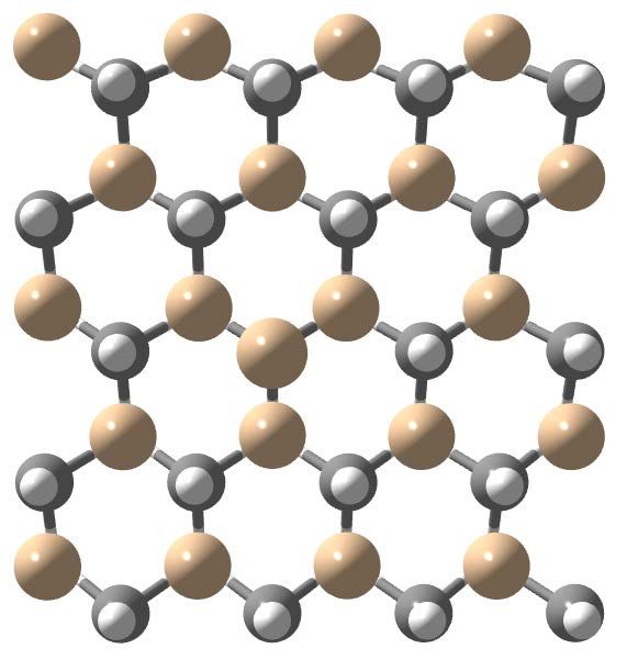
Quantum point defects in 2D materials: The QPOD database                                                                                        5

                     q+1
                                                                                                                                CBM
         λq+1

                                               εH (q + 0.5; Rq )
                                                                                                    q−1
Energy

                                                                                                                                           EF
                            ε (q/q + 1)
                                                                                                                   λq−1

                                                                   εH (q − 0.5; Rq )

                                                                                         ε (q/q − 1)
                                          q

                                                                                                                                VBM

                                                           ∆Q

Figure 3. Schematic view of the SJ approach to calculate charge transition levels. Left: the optical charge transition
levels are calculated starting from a given charge state q by either adding (i.e. q − 0.5) or removing (i.e. q + 0.5) half an electron
and calculating the HOMO energies at frozen atomic configuration (i.e. εH q ± 0.5; Rq , light colored arrows in left panel). Due
to ionic relaxations one has to correct with the reorganization energies λq±1 to reduce the energy cost for the transition wrt. EF .
Right: the reorganization energy for adding (removing) an electron has to be added (subtracted)     from the optical transition levels
(see red arrows in the right panel) in order to compute the thermodynamic CTLs ε q/q ± 1 .

     It has been shown for defects in bulk materials                                   equilibrium is then determined self-consistently from
that the CTLs obtained from SJ theory are in good                                      a requirement of charge neutrality[55]
agreement with results obtained from total energy                                      XX
                                                                                               qC[Xq ] = n0 − p0                          (8)
differences[51, 53].      For 2D materials, a major
                                                                                       X        q
advantage of the SJ method is that it circumvents the
issues related to the electrostatic correction, because it                             where the sum is over structural defects X in charge
completely avoids the comparison of energies between                                   states q, and n0 and p0 are the electron and hole carrier
supercells with different number of electrons. The                                     concentrations, respectively. The latter are given by
                                                                                             Z ∞
Kohn-Sham eigenvalues of a neutral or (partially)
                                                                                       n0 =        dEf (E)ρ(E),                              (9)
charged defect supercell are referenced relative to the                                                Egap
electrostatic potential averaged over the PAW sphere of                                          Z     0
an atom located as far as possible away from the defect                                p0 =                 dE[1 − f (E)]ρ(E)              (10)
site (typically around 7 Å depending on the exact size                                                −∞
of the supercell). By performing the potential average                                 where ρ(E) is the local    density of states, f (E) =
over an equivalent atom of the pristine 2D layer, we
                                                                                       1/ exp (E − EF )/kB T is the Fermi-Dirac distribution,
can reference the Kohn-Sham eigenvalue of the defect                                   and the energy scale is referenced to the valence band
supercell to the VBM of the pristine material. As                                      maximum of the pristine crystal.
an alternative to averaging the potential around an                                          Under the assumption that all the relevant defects,
atom, the asymptotic vacuum potential can be used as                                   i.e. the intrinsic defects with the lowest formation
reference. We have checked that the two procedures                                     energies, are accounted for, Eq. (8) will determine
yield identical results (usually within 0.1 eV), but                                   the Fermi level position of the material in thermal
prefer the atom-averaging scheme as it can be applied                                  equilibrium. The equilibrium Fermi level position
to bulk materials as well.                                                             determines whether a material is intrinsically p-doped,
                                                                                       n-doped, or intrinsic. The three different cases are
2.4. Equilibrium defect concentrations                                                 illustrated schematically in Fig. 4. For the n-type
According to Eqs. (3) and (4), the formation energy                                    case (left panel), the most stable defect is D1 in charge
of charged defects, and therefore their equilibrium                                    state +1. Thus, charge carriers are transferred from
concentration, is a function of the Fermi level.                                       the defect into the conduction band resulting in a
The Fermi level position of the system in thermal                                      Fermi level just below the CBM. Similarly, for the p-
                                                                                       type case (middle panel) the defect D1 in charge state
Quantum point defects in 2D materials: The QPOD database                                                                      6

                            n − type                         p − type                               intrinsic
                            D1         D3
              3             D2         EF

              2
  E f [eV]

                  VBM

                                                   VBM

                                                                                         VBM
                                             CBM

                                                                                  CBM

                                                                                                                        CBM
              1

              0

             −1
                    0.0    0.5   1.0   1.5           0.0    0.5      1.0    1.5             0.0    0.5    1.0     1.5
                          E − EVBM [eV]                    E − EVBM [eV]                          E − EVBM [eV]

Figure 4. Intrinsic dopability of defect systems. Formation energies with respect to the standard states as a function of
energy for three mock-sytems with three defect types present, respectively. Left: n-type dopable regime (EF close to CBM) with
dominating donor defect. Middle: p-type dopable regime (EF close to VBM) with dominating acceptor defect. Right: intrinsic
material (neither p- nor n-dopable due to the presence of competing acceptor and donor defects.)

−1 is the most stable. Consequently, charge carriers              vector Γ(R) can be expanded in the character vectors,
are promoted from the valence band into the defect                χ(α) (R),
resulting in EF close to the VBM. In the right panel,                     X
donor and acceptor states are competing, which results            Γ(R) =     cα χ(α) (R)                          (12)
                                                                           α
in an effective cancelling of the p- and n-type behavior,
pinning the Fermi level in the middle of the band gap.            where the quantity cα represents the fraction of ψn
In Section 4.3 we analyse the intrinsic carrier types and         that transforms according to the irrep α. For any well
concentrations of 58 host materials where we set gXq              localised defect state, all the cα will be zero except one,
and NX in Eq. (4) to one.                                         which is the irrep of the state. In general, less localised
                                                                  states will not transform according to an irrep of G.
                                                                  That is because the wave functions are calculated in the
2.5. Symmetry analysis
                                                                  symmetry-broken supercell, see Sec. 2.1, and therefore
All states with an energy in the band gap are classified          will have a lower symmetry than the defect. To exclude
according to the symmetry group of the defect                     such low-symmetry tails on the wave functions, the
using a generalization of the methodology previously              integral in Eq. (11) is truncated beyond a cut-off radius
implemented in GPAW for molecules [56]. In a first                measured from the center of symmetry of the defect.
step, the point group, G, of the defect is determined.                 As an example, Figure 5 shows the coefficients
To determine G we first reintroduce the relaxed defect            cα for the in-gap states of the (neutral) sulfur
into a supercell that preserves the symmetry of the               vacancy in MoS2 . This is a well studied prototypical
host material; precisely, a supercell with basis vectors          defect with C3v symmetry.           The absence of the
defined by setting n1 = m2 = n and n2 = m1 = 0                    chalcogen atom introduces three defect states in the
in Eqs. (1, 2). We then use spglib[57] to obtain G as             gap: a totally symmetric a1 state close to the VBM
the point group of the new supercell. We stress that              and two doubly degenerate mid-gap states (ex , ey ).
the high-symmetry supercell is only used to determine             The symmetry coefficients cα correctly captures the
G while all actual calculations are performed for the             expected symmetry of the states[46], at least for
low-symmetry supercell as described in Sec. 2.5.                  small cut-off radii.        The effect of employing a
     The defect states in the band gap are labeled                symmetry-broken supercell can be seen on the totally
according to the irreducible representations (irrep) of           symmetric state a1 , which starts to be mixed with the
G. To obtain the irrep of a given eigenstate, ψn (r), we          antisymmetric a2 irrep as a function of the radius, while
form the matrix elements                                          there is no effect on the degenerate ex state. Therefore
                                                                  a radius of 2 Å is used in the database to catch the
                   Z
Γ(R) = Γnn (R) = dr ψn (r)∗ R ψn (r)                (11)          expected local symmetry of the defect.
where R is any symmetry transformation of G. It
follows from the orthogonality theorem[58] that the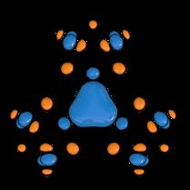
Quantum point defects in 2D materials: The QPOD database                                                                             7

       1.0

       0.8
                                                       εex = 1.26 eV                               εey = 1.27 eV
       0.6                                                                              a1
  cα

                                εa1 = 0.15 eV                                           a2
       0.4                                                                              e

       0.2

       0.0

               2         4        6        8             2        4           6         8           2        4       6        8
                   Cut-off radius [Å]                       Cut-off radius [Å]                        Cut-off radius [Å]

Figure 5. Orbital symmetry labels for different cutoff radii. All defect states with an energy inside the band gap of the
host material are classified according to the irreps of the point group of the defect. The cα coefficient is a measure of the degree to
which a defect state transforms according to irrep α. Performing the symmetry analysis within a radius of a few Å of the center of
symmetry leads to a correct classification of the totally symmetric a1 state and the degenerate ex and ey states of the neutral sulfur
vacancy in MoS2 . The isosurfaces of the orbitals are shown as insets and the energy eigenvalues reference to the VBM.

2.6. Transition dipole moment                                          in the excited state. Since this step is not part of our
                                                                       general workflow, but is only performed for selected
The transition dipole moment is calculated between all
                                                                       defects, radiative lifetimes are currently only available
single particle Kohn-Sham states inside the band gap,
                                                                       for a few transitions.
                       i~ hψn | p̂ |ψm i
µnm = hψn | r̂ |ψm i =                   ,           (13)
                       me εn − εm                                      2.8. Hyperfine coupling
where r̂ is the dipole operator, p̂ is the momentum
                                                                       Hyperfine (HF) coupling refers to the interaction
operator, and me is the electron mass. The transition
                                                                       between the magnetic dipole associated with a nuclear
dipole moment yields information on the possible
                                                                       spin, ÎN , and the magnetic dipole of the electron-spin
polarization directions and oscillator strength of a
                                                                       distribution, Ŝ. For a fixed atomic nuclei, N , the
given transition. In this work, the transition dipoles
                                                                       interaction is written
between localised defect states are calculated in real
                                                                                    Ŝi AN IˆN
                                                                                X
space, i.e. using the first expression in Eq. (13), after              Ĥ N =
                                                                         HF                 ij j                           (15)
translating the defect to the center of the supercell.                            i,j

                                                                       where the hyperfine tensor AN is given by
2.7. Radiative recombination rate and life time
                                                                               2α2 ge me
                                                                                          Z
                                                                       ANij =                δT (r)ρs (r)dr
Radiative recombination refers to the spontaneous                                3MN
decay of an electron from an initial high energy state                                                                       (16)
                                                                              α2 ge me      3ri rj − δij r2
                                                                                        Z
to a state of lower energy upon emitting a photon. The                      +                               ρ s (r)dr.
                                                                               4πMN                r5
rate of a spin-preserving radiative transition between
an initial state ψm and a final state ψn is given by [59]              The first term represents the isotropic Fermi-contact
                                                                       term, which results from a non-vanishing electron spin
                    3                                                  density ρs (r) at the centre of the nucleus. δT (r) is a
                  EZPL  µ2nm
Γrad
 nm = 1/τrad =                .                      (14)              smeared out δ-function which appears in place of an
                   3π0 c3 ~4                                          ordinary δ-function in the non-relativistic formulation
Here, 0 is the vacuum permitivity, EZPL is the                        of the Fermi-contact term and regulates the divergence
zero phonon line (ZPL) energy of the transition (see                   of the s-electron wave function at the atomic core[60].
Sec. 2.10), and µnm is the transition dipole moment                    α is the fine structure constant, me is the electron mass,
defined in Eq. (13). The ZPL energy includes                           MN is the mass of atom N , and ge is the gyromagnetic
the reorganisation energy due to structural differences                ratio for electrons. The second term represents the
between the initial and final states, which can be on the              anisotropic part of the hyperfine coupling tensor and
order of 1 eV. Consequently, an accurate estimate of                   results from dipole-dipole interactions between nuclear
the radiative lifetime requires a geometry optimisation                and electronic magnetic moments.
Quantum point defects in 2D materials: The QPOD database 8
CBM CBM CBM
Energy [eV]
EF EF EF
VBM VBM VBM
doublet triplet singlet
Figure 7. Possible occupancies resulting in different spin
Figure 6. Iso-surface of the calculated spin-density (isovalue of configurations of the defect systems for the excited state
−3 calculations. The states involved in the excitation are encircled
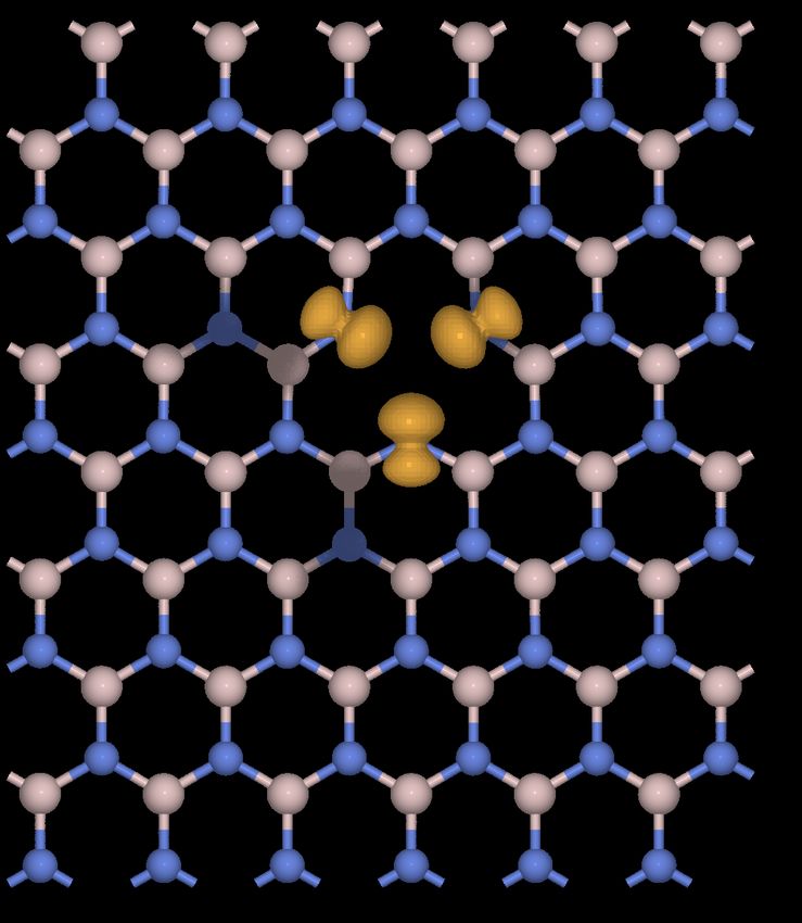
0.002 |e|Å ) for the V−
B defect in hexagonal boron nitride. red.
Ä ä
The Fermi-contact term a = Tr AN /3 depends describes the splitting between the ms = ±1 and ms =
only on the l = 0 component of the spin density at the 0 magnetic sub-levels, while E describes the splitting
nucleus. In contrast, the anisotropic term AN ij − a is of the ms = ±1 sub-levels. D is generally zero for a
sensitive to the l > 0 components of the spin density spherically symmetric wave function because there is
near the nucleus. The hyperfine tensor thus provides no direction in which electrons of a triplet can move
direct insight into the electron spin distribution near to minimize the repulsive dipole-dipole interaction.
the corresponding nucleus, and a direct comparison However, for non-spherical wave functions, D will be
of the calculated HF coupling constants with electron non-zero and lift the degeneracy of magnetic sub-levels
paramagnetic resonance spectroscopy measurements ms = 1 and ms = 0. A positive value of D will result
can help to identify the nature of defect centers[31, 26]. from an oblate spin-distribution, while a negative value
As an illustration, Figure 6 shows the iso-surface of will result from a prolate spin-distribution. The value
the spin density of the V− B defect in hexagonal boron of E will be zero for axially symmetric wave functions.
nitride.
In the present work, the AN tensors are calculated 2.10. Excited states
for all atoms of the supercell, and its eigenvalues, also
known as the HF principal values, are reported in the In Kohn-Sham DFT, excited electronic states can
QPOD database. be found by solving the Kohn-Sham equations with
non-Aufbau occupations of the orbitals. Often this
2.9. Zero field splitting approach is referred to as the delta self-consistent
field (Delta-SCF) method[61]. The excited state
Zero field splitting (ZFS) refers to the splitting of solutions are saddle points of the Kohn-Sham energy
magnetic sub levels of a triplet defect state due to the functional. Unfortunately, the Delta-SCF approach
magnetic dipole-dipole interaction of the two electron often struggle to find such solutions, especially when
spins that takes place even in the absence of an external nearly degenerate states are involved. The Delta-SCF
magnetic field. A triplet (S = 1) defect state can be method fails in particular for cases involving charge
described by a spin Hamiltonian of the following form transfer or Rydberg states [40]. This is due to a
X significant rearrangement of charge density between
ĤZFS = Ŝi Dij Ŝj , (17)
orbitals with similar energy.
ij
Therefore, in the present work we use an
where Ŝ is the total spin operator and D is the ZFS alternative to the conventional Delta-SCF method,
tensor given by namely a method based on the direct optimization
2
α ge me
Z
3ri rj − δij r 2 (DO) of orbital rotations by means of an efficient quasi-
Dij = |φij (r1 , r2 )|2 dr 1 r2 . (18) Newton method for saddle points, in combination with
4π r5
the maximum overlap method (MOM)[40]. The MOM
Eq. (17) can also be written as ensures that the character of the states is preserved
ĤZFS = Dxx Ŝx2 + Dyy Ŝy2 + Dzz Ŝz2 during the optimization procedure. In the DO-MOM
method, convergence towards the n-th order saddle
= D(Ŝz2 − S(S + 1)/3) + E(Ŝx2 − Ŝy2 ), (19)
point is guided by an appropriate pre-conditioner based
where D = 3Dzz /2 and E = (Dxx − Dyy )/2 are called on an approximation to the Hessian with exactly n
axial and rhombic ZFS parameters, respectively. D negative eigenvalues. This method ensures fast andQuantum point defects in 2D materials: The QPOD database 9
robust convergence of the excited states, as compared
to conventional Delta-SCF [40] methods. Ee
The DO-MOM method has been previously used
for the calculation of excited state spectra of molecules
[40]. However, this work is the first application of the
absorption
method to defect states. We have benchmarked the λe
emission
Energy [eV]
method for a range of point defects in diamond, hBN,
SiC, and MoS2 , and established that the method yields
ZPL
results in good agreement with conventional Delta-SCF
calculations. Eg
The most frequently occurring point defect spin
configurations are sketched in Fig. 7. For the
doublet and triplet spin configuration, both the λg
ground and excited states can be expressed as single
Slater determinants. However, for the singlet spin ∆Q
configuration, the ground state is a closed shell singlet,
while the excited state, as a result of the single Coordinate Q [amu1/2 Å]
excitation in either spin channel, will result in an
open shell singlet state, which cannot be expressed as Figure 8. Schematic CC diagram of a ground state
a single Slater determinant. This open shell singlet to excited state transition. Absorption and emission to
state can, however, be written as a sum of two Slater and from the excited state (blue, orange) as well as their
determinants of the form |a ↑, b ↓i and |a ↓, b ↑i, each of respective reorganization energies λe,g as a function of energy
and configuration coordinate Q. The zero phonon line transition
which represent a mixed singlet-triplet state accessible (ZPL) is visualized in green.
with Delta-SCF. This allows us to obtain the singlet
energy as
Es = 2Est − Et . (20) above electron-phonon spectral function is fed into a
generating function to produce the photoluminescence
Here, Est is the DFT energy calculated by setting the lineshape[62].
occupancy for the open-shell singlet state, while Es and
Et are the energies of the corresponding singlet and
triplet states. Note that the latter can be represented 3. QPOD workflow and database
as a Slater determinant.
3.1. The QPOD workflow
Photoluminescence spectra of selected point
defects were calculated using a generating function The backbone of the QPOD database is represented
approach[62] outlined below. First, the mass weighted by a high-throughput framework based on the Atomic
difference between atomic coordinates in the ground Simulation Recipes (ASR) [29] in connection with
and excited electronic states is computed as follows the MyQueue [30] task and workflow scheduling
X system. Numerous recipes, designed particularly
∆Q = mα ∆Rα2, (21) for the evaluation of defect properties, have been
α
implemented in ASR and have been combined in a
where the sum runs over all the atoms in the central MyQueue workflow to generate all data for the
supercell. Afterwards, the partial Huang-Rhys factors QPOD database.
are computed as The underlying workflow is sketched in Fig. 9,
1 and will be described briefly in the following. As
Sk = ωk Q2k , (22)
2~ a preliminary step the C2DB [32, 33] is screened to
where Qk is the projection of the lattice displacement obtain the set of host materials. Only non-magnetic,
on the normal coordinates of the ground state thermodynamically and dynamically stable materials
described by phonon mode k. The electron-phonon PBE
with a PBE band gap of Egap > 1 eV are selected as
spectral function, which depends on the coupling host materials. These criteria result in 281 materials of
between lattice displacement and vibrational degrees which we select 82 from a criterion of Ne × Vsupercell <
of freedom, is then obtained by summing over all the 0.9 Å3 combined with a few handpicked experimentally
modes k known and relevant 2D materials (MoS2 , hBN, WS2 ,
MoSe2 ). It is important to mention, that some host
X
S(ω) = Sk δ(ω − ωk ). (23)
k materials exist in different phases (same chemical
The integral over the electron-phonon spectral function formula and stoichiometry, but different symmetry),
gives the (total) HR factor of the transition. The e.g. 2H-MoS2 and 1T-MoS2 . In these cases we onlyQuantum point defects in 2D materials: The QPOD database 10
Identifying Host The Defect Workflow - Overview In progress …
Materials Empty Excited state
Y
C2DB state(s) workflow
in gap (neutral)
N
Band gap > 1 eV
Non-magnetic Ground state N Filled Y Data
High stability workflow state(s) extraction
(neutral) in gap workflow
q+1
host DB
N Y Ground state
State(s) results-
workflow
Create native in gap? asr.*.json
(charged)
point defects
q-1
Determine
N All q
defect
done? QPOD
supercells
database
Ground State Excited State Data Extraction
Workflow Workflow Workflow
Relax structure (in Is KS EL/H transition Thermodynamics
neutral state/charge between defect states Ef, CTLs, defect
state q) larger than 0.5 eV? concentrations
Symmetries
Obtain ground state Set up excited state
Structural, one-
density calculation
electron states
Evaluate defect states Misc
Calculate PL-lineshape,
inside the pristine HF-coupling, ZFS,
ZPL, HR factor, etc.
bandgap spin-coherence time
Set up SJ calculation / Data Collection and Visualization
do DFT calculation
with half-integer q
QPOD metadata visualization web application
Figure 9. The workflow behind the defect database. First, starting from C2DB suitable host materials are identified. With
the ASR recipe for defect generation the defect supercells are set up and enter the ground state workflow for neutral systems.
Afterwards, depending on the nature of the defect states inside the gap, charged calculations are conducted within the charged
ground state workflow. If all charged calculations for a specific system are done (|q| < 3), physical results are collected using the
data extraction workflow and thereafter saved in the defect database. The database is equipped with all necessary metadata, and
together with various visualization scripts the browseable web application is created. The excited state workflow is executed for
selected systems as discussed in Sec. 4.7.Quantum point defects in 2D materials: The QPOD database 11
keep the most stable one, i.e. 2H-MoS2 for the previous 3.3. The QPOD webapp
example.
A defining feature of the QPOD database is its easy
For each host material, all inequivalent vacancies
accessibility through a web application (webapp). For
and antisite defects are created in a supercell as
each row of the database, one can browse a collection of
described in Sec. 2.1. Each defect enters the ground
web-panels designed to highlight the various computed
state workflow, which includes relaxation of the neutral
properties of the specific defect. Specific elements
defect structure, calculation of a well-converged ground
of the web-panels feature clickable ”?” icons with
state density, identification and extraction of defect
explanatory descriptions of the content to improve the
states within the pristine band gap, and SJ calculations
accessibility of the data.
with half-integer charges q. If there are no states
Directing between different entries of the database
within the gap, the defect system directly undergoes
is either possible by using hyperlinks between related
the data extraction workflow and is stored in the
entries, or using the overview page of the database,
QPOD database.
where the user can search for materials, and order them
For systems with in-gap states above (below)
based on different criteria. Furthermore, we ensure the
EF , an electron is added (removed) and the charged
direct connection to C2DB with hyperlinks between
structures are relaxed, their ground state calculated
a defect material and its respective host material
and the states within the band gap are examined again
counterpart in C2DB in case users want to find more
up to a maximum charge of +3/−3. Once all charge
information about the defect-free systems.
states have been relaxed and their ground state density
has been evaluated, the data extraction workflow is
executed. Here, general defect information (defect 3.4. Overview of host materials
name, defect charge, nearest defect-defect distance, In total, 82 host crystals that were chosen according to
etc.), charge transition levels and formation energies, the criteria outlined in Sec. 3.1 comprise the basis of
the equilibrium self-consistent Fermi level, equilibrium our systematic study of intrinsic point defects. The set
defect concentrations, symmetries of the defect states of host materials span a range of crystal symmetries,
within the gap, hyperfine coupling, transition dipole stoichiometries, chemical elements, and and band gaps
moments, etc. are calculated and the results are stored (see Fig. 10). Among them, at least nine have already
in the database. The data is publicly available and easy been experimentally realized in their monolayer form,
to browse in a web-application as will be described in namely As2 , BN, Bi2 I6 , C2 H2 , MoS2 , MoSe2 , Pd2 Se4 ,
Sec. 3.3. WS2 , and ZrS2 whereas 15 possess an ICSD [64, 65]
We note, that selected systems have been subject entry and are known as layered bulk crystals. The PBE
to excited state calculations in order to obtain ZPL band gaps range from 1.02 eV for Ni2 Se4 up to 5.94
energies, PL spectra, HR factors, etc. enabling the eV for MgCl2 making our set of starting host crystals
identification of promising defect candidates for optical particularly heterogeneous.
applications as is discussed in Sec. 4.7.
4. Results
3.2. The QPOD database
The QPOD database uses the ASE DB format [63] In this section we first present some general illustra-
which currently has five backends: JSON, SQLite3, tions and analyses of the data in QPOD. We then
PostgreSQL, MySQL, MariaDB. An ASE DB enables leverage the data to address three specific scientific
simple querying of the data via the in-built ase db problems, namely the identification of: (i) Defect tol-
command line tool, a Python interface, or a webapp erant semiconductors with low concentrations of mid-
(see Sec. 3.3). With those different possibilities to gap states. (ii) Intrinsically p-type or n-type semicon-
access and interact with the data, we aim to give users ductors. (iii) Optically accessible high-spin defects for
a large flexibility based on their respective technical quantum technological applications.
background and preferences.
Each row of QPOD is uniquely defined by defect 4.1. Relaxation of defect structures
name, host name, and it’s respective charge state. A major part of the computational efforts to create the
Furthermore, the fully relaxed structure as well as QPOD went to the relaxation of the defect structures in
all of the data associated with the respective defect a symmetry broken supercell. As discussed in Section
is attached in the form of key-value pairs or JSON- 2.1 the strategy to actively break the symmetry of the
formatted raw data. host crystal by the choice of supercell was adopted
to enable defects to relax into their lowest energy
configuration.Quantum point defects in 2D materials: The QPOD database 12
PBE
Figure 11 shows the gain in total energy due
Ehull Egap
to the relaxation for the over 1900 vacancy and
Ag2 Br2 Se4 -1 antisite defects (different charge states included). Not
Ag2 Cl2 Se4 -1
Al2 Br2 Se2 -59 unexpectedly, the relaxation has the largest influence
Al2 Cl2 S2 -59
Al2 Cl6 -162 on antisite defects while vacancy structures in general
Al2 S2 -187
Al2 Se2 -187 show very weak reorganization relative to the pristine
As2 -164
AsClS-156 structure as can be seen in the left panel of Fig. 11.
AsClSe-156 The relaxations for charged defects have always been
Au2 MoO4 -1
Au2 WO4 -1 started from the neutral equilibrium configuration of
BN-187
BaCl2 -164 the respective defect. As a result, the reorganization
Bi2 I6 -147
C2 H2 -164 energies for charged defects is significantly lower (see
CH2 Si-156
CaBr2 -164 right panel of Fig. 11).
CaCl2 -164
CdCl2 -164
CdI2 -115
Co2 Cl6 -162 4.2. Charge transition levels
Cs2 Br2 -129
Cs2 Cl2 -129
FeZrCl6 -1 In Section 2.3 we described how we obtain the
Ga2 Cl2 O2 -59
Ga2 Cl6 -162 CTLs by combining Slater-Janak transition state
Ge2 S2 -31
GeO2 -164 theory on a static lattice with geometry relaxations
GeS2 -115
GeTe-156
H2 Si2 -164
in the final
state. For ”negative” transitions, e.g.
HfZr3 S8 -1
HgBr2 -115
ε 0/ − 1 , the effect of the relaxation is to lower
I6 Sb2 -162 the energy cost of adding the electron, i.e. the
K2 Br2 -129
K2 Cl2 -129 reorganisation energy lowers the CTL. In contrast, the
K2 I2 -129
Li2 H2 O2 -129 lattice relaxations should produce an upward shift for
Li2 H2 S2 -1
MgBr2 -164 ”positive” transitions, e.g. ε 0/ + 1 , because in this
MgCl2 -164
MgH2 O2 -164 case the CTL denotes the negative of the energy cost
MgH2 S2 -1
MgI2 -164 of removing the electron.
MoS2 -187
MoSe2 -187 Figure 12 shows the ε 0/ + 1 and ε 0/ − 1
Na2 H2 O2 -11
Na2 H2 S2 -1 CTLs for a small subset of defects. Since the energies
Ni2 Se4 -14 are plotted relative to the vacuum level, the CTLs
NiO2 -164
Pb2 S2 -6 correspond to the (negative) ionisation potential (-
PbCl2 -164
Pd2 S4 -14 IP) and electron affinity (EA), respectively. Results
Pd2 Se4 -14
PdO2 -164 are shown both with and without the inclusion of
Rb2 Br2 -129
Rb2 Cl2 -129 relaxation effects. As expected, the relaxation always
Rb2 I2 -129
Rh2 Cl6 -162 lowers the EA and the IP (the ε 0/ + 1 is always
S2 Si-5
Sc2 Br2 S2 -59 raised). The reorganisation energies can vary from
Sc2 Cl2 O2 -59
Sc2 Cl2 S2 -59 essentially zero to more than 2 eV, and are absolutely
Sc2 Cl2 Se2 -59
Sc2 Cl6 -162 crucial for a correct prediction of CTLs and (charged)
SnO2 -164
SnSe-156 defect formation energies.
SnTe-156
SrBr2 -164 We notice that the CTLs always fall inside the
SrCl2 -164
Ti2 O4 -11 band gap of the pristine host (marked by the grey
Ti2 O6 -59
WS2 -187 bars) or very close to the band edges. This is clearly
Y2 I6 -162
ZnBr2 -115 expected on physical grounds, as even for a defective
ZnCl2 -115 system the CTLs cannot exceed the band edges (there
ZnF2 -115
ZnH2 O2 -12 are always electrons/holes available at the VBM/CBM
ZnI2 -115
Zr2 O6 -59 sufficiently far away from the point defect). However,
ZrS2 -164
for small supercells such behavior is not guaranteed as
0.3 0.15 0 3 6
the band gap of the defective crystal could deviate from
Energy [eV]
that of the pristine host material. Thus, the fact that
the CTLs rarely appear outside the band gap is an
Figure 10. Overview of host crystals. Energy above convex indication that the employed supercells are generally
hull in eV/atom Ehull (purple bars, left) and PBE-calculated large enough to represent an isolated defect.
PBE (yellow bars, right) of the 82 host crystals of
band gap Egap When the Fermi level is moved from the VBM to
QPOD. Host materials which have been realized experimentally
the CBM one expects to fill available defects states
(in their monolayer form) are highlighted in green and materials
with a known layered bulk phase and related ICSD [64, 65] entry with electrons
in a stepwise
manner, i.e. such that
are shown with a hatch pattern. ε q + 1/q < ε q/q − 1 . In particular, we expect
−IP < EA. Interestingly, for a few systems, e.g.Quantum point defects in 2D materials: The QPOD database 13
150
Vacancies Vacancies
Neutral defects Antisites
400 Charged defects Antisites
100 300
Count
200
50
100
0 0
0 1 2 3 4 5 0.0 0.2 0.4 0.6 0.8 1.0
Etot (0; Rinitial ) − Etot (0; R0 ) [eV] Etot (q 0 ; R0 ) − Etot (q 0 ; Rq0 ) [eV]
Figure 11. Relaxation effects for the formation of charged and neutral defects. Left: histogram of the reorganization
energy from the initial defect substitution to the neutral equilibrium configuration. Low values on the x-axis correspond to small
reorganization of defect structures upon addition of a defect to the pristine host crystal. Right: histogram of the reorganization
energy between a neutral defect and its charged counterpart.
0
−2
E − Evac [eV]
−4
−6 -IP w/ relax: (0/+1)
EA w/ relax: (0/-1)
-IP w/o relax: (0/+1)
−8
EA w/o relax: (0/-1)
IK in K2 I2
KI in K2 I2
VI in K2 I2
VK in K2 I2
CdI in CdI2
ICd in CdI2
VI in CdI2
ZnBr in ZnBr2
VBr in ZnBr2
ZnF in ZnF2
VF in ZnF2
IZn in ZnI2
ZnI in ZnI2
VI in ZnI2
VZn in ZnI2
CaBr in CaBr2
VCa in CaBr2
GeO in GeO2
OGe in GeO2
VO in GeO2
ClPb in PbCl2
PbCl in PbCl2
VCl in PbCl2
VPb in PbCl2
SW in WS2
AlCl in Al2 Cl6
ClAl in Al2 Cl6
VCl in Al2 Cl6
SnTe in SnTe
TeSn in SnTe
VSn in SnTe
VTe in SnTe
Figure 12. Relaxation effects for ionisation potentials and electron affinities. Energies of -IP (red symbols) and EA
(blue symbols) with and without relaxation effects included (boxes and crosses, respectively). The energies are all referenced to the
vacuum level of the pristine crystal and grey bars represent the valence/conduction band of the individual host crystals.
VF in ZF2 , the ordering of IP and EA is inverted. devices[67], or photo detectors[68], the question of
The physical interpretation of such an ordering is that dopability of the semiconductor material is crucial.
the neutral charge state becomes thermodynamically Modulation of the charge carrier concentration is a
unstable with respect to positive and negative charge highly effective means of controlling the electrical and
states [21]. This results in a direct transition from optical properties of a semiconductor. This holds
positive to negative charge state in the formation in particular for 2D semiconductors whose carrier
energy diagram. concentrations can be modulated in a variety of ways
including electrostatic or ionic gating[69, 70], ion
4.3. Intrinsic carrier concentrations intercalation[71], or surface functionalisation[72]. In
general, these methods are only effective if the material
For many of the potential applications of 2D is not too heavily doped by its ubiquitous native
semiconductors, e.g. transistors[66], light emitting defects, which may pin the Fermi level close to oneQuantum point defects in 2D materials: The QPOD database 14
of the band edges. For applications relying on high
carrier conduction rather than carrier control, a high
10−1 101 103 105 107 109 1011
intrinsic carrier concentration may be advantageous - −2
at least if the native defects do not degrade the carrier n0 [cm ]
mobility too much, see Sec. 4.6.
Ag2 Br2 Se4
Figure 13 shows the calculated position of the Sc2 Cl2 Se2
equilibrium Fermi level (at room temperature) for ZrS2
Co2 Cl6
all the 2D materials considered as defect hosts in Rh2 Cl6
this work. It should be noted that the Fermi level GeTe
position depends on the number of different defect Ni2 Se4
Pd2 Se4
types included in the analysis. Consequently, the WS2
results are sensitive to the existence of other types MoS2
p-type SnTe n-type
of intrinsic defects with formation energies lower than S2 Si
or comparable to the vacancy and antisite defects Pd2 S4
GeS2
considered here. Fermi level regions close to the VBM Al2 Se2
or CBM (indicated by red/blue colors) correspond to Sc2 Cl2 S2
Sc2 Br2 S2
p−type and n−type behavior, respectively, while Fermi SnSe
levels in the central region of the band gap correspond I6 Sb2
Au2 MoO4
to intrinsic behavior. CH2 Si
Clearly, most of the materials present in the HgBr2
QPOD database show either intrinsic or n-type Ge2 S2
ZnI2
behavior. An example of a well known material with Bi2 I6
intrinsic behavior is MoS2 , where native defects pin the CdI2
Ag2 Cl2 Se4
Fermi level deep within the band gap resulting in very
VBM
CBM
SnO2
low electron and hole carrier concentrations in good PbCl2
Li2 H2 S2
agreement with previous observations[73, 74, 75, 46]. Au2 WO4
As an example of a natural n-type semiconductor we Rb2 I2
Al2 Cl6
highlight the Janus monolayer AsClSe, which presents GeO2
an impressive electron carrier concentration of 9.5 × Ga2 Cl2 O2
Ga2 Cl6
1011 cm−2 at 300 K, making it an interesting candidate CdCl2
for a high-conductivity 2D material. For the majority Sc2 Cl6
of the materials, the equilibrium carrier concentrations Na2 H2 O2
K2 I 2
are in fact relatively low implying a high degree ZnCl2
of dopability. We note that none of the materials Rb2 Br2
ZnF2
exhibit intrinsic p-type behavior. This observation K2 Br2
indicates that the challenge of finding naturally p- BN
Rb2 Cl2
doped semiconductors/insulators, which is well known Na2 H2 S2
for bulk materials[76, 77, 78, 79], carries over to the MgBr2
K2 Cl2
class of 2D materials. CaBr2
SrBr2
BaCl2
4.4. Defect formation energies: Trends and SrCl2
correlations CaCl2
MgCl2
intrinsic AsClS
The formation energy is the most basic property of MgH2 S2
a point defect. Figure 14 the distribution of the AsClSe
calculated formation energies of neutral defects for 0.00 0.25 0.50 0.75 1.00
both vacancy (blue) and antisite (orange) defects. (EFsc − EVBM )/Egap
For the chemical potential appearing in Eq. (3) we
used the standard state of each element. There is
essentially no difference between the two distributions, Figure 13. Self-consistent Fermi-level position for host
and both means (vertical lines) are very close to 4 eV. materials within the pristine band gap. The energy scale
Roughly half (44 %) of the neutral point defects have is normalized with respect to each individual pristine band gap.
The regions close to the CBM, VBM correspond to the p-, n-
a formation energy below 3 eV and 28 % are below 2
type dopable regimes, respectively. The colorcode of the markers
eV. This implies that many of the defects would form represents the equilibrium electron carrier concentration n0 .
readily during growth and underlines the importance of
including intrinsic defects in the characterization of 2DQuantum point defects in 2D materials: The QPOD database 15
Vacancies 150
30
Antisites
Count
100
Count
20
50
10
0
0 C1 Cs Ci C2 C2h C2v C3v C4v D2d D3 D3d
0 2 4 6 8 10
Figure 15. Distribution of point groups for relaxed
0.0 defects. Point groups are ordered from the lowest symmetry
group (i.e. C1 ) to the highest occurring symmetry group (D3d ).
5
−0.5
∆Hhost [eV]
Egap [eV]
−1.0 4
of (specific types of) defects are required for many color
−1.5 3 center-based quantum technology applications.
−2.0 2 4.5. Point defect symmetries
−2.5 Another basic property of a point defects is its local
0 2 4 6 8 10 symmetry, which determines the possible degeneracies
E f [eV] of its in-gap electronic states and defines the selection
rules for optical transitions between them. Figure 15
shows the distribution of point groups (in Schönflies
Figure 14. Distribution of defect formation energies notation) for all the investigated neutral defect
in the neutral charge state. Top: histogram of neutral systems. A large fraction of the defects break all
formation energies E f wrt. standard states for vacancy and
antisite defects. The vertical lines represent the mean value. the symmetries of the host crystal (34 % in C1 )
Bottom: heat of formation ∆Hhost of the pristine monolayer as or leave the system with only a mirror symmetry
a function of the neutral formation energies with the pristine (20 % in Cs). A non-negligible number (31 %)
PBE-calculated band gap as a color code.
of defects can be characterized by 2, 3, or 4-fold
rotation axis with vertical mirror planes (C2v , C3v
materials. As a reference, the NV center in diamond and C4v ). Naturally, C3v defects (20 % overall) often
shows formation energies on the order of 5 eV to 6 stem from hexagonal host structures, some examples
eV[80] (HSE value). being VS and WS in WS2 , VSe in SnSe, and CaBr
The lower panel of Figure 14 shows the defect in CaBr2 . Such defects share the symmetry group of
formation energy relative to the heat of formation of the well known NV center in diamond[81] and might
the pristine host material, ∆Hhost . There is a clear be particularly interesting candidates for quantum
correlation between the two quantities, which may not technology applications. Relatively few defect systems
come as a surprise since the ∆Hhost measures the (3 %) incorporate perpendicular rotation axes, e.g. the
gain in energy upon forming the material from atoms D3 symmetry of ISb in I6 Sb2 .
in the standard states. More stable materials, i.e. Adding or removing charge to a particular defect
materials with more negative heat of formation, are system can influence the structural symmetry as it was
thus less prone to defect formation than less stable previously observed for the negatively charged sulfur
materials. It is also interesting to note the correlation vacancy in MoS2 [82]. We find that 10 % of the defects
with the band gap of the host material, indicated by in QPOD undergo a change in point group when adding
the color of the symbols. A large band gap is seen (removing) an electron to (from) the neutral structure
to correlate with a large (negative) ∆Hhost and large and relaxing it in its respective charge state.
defect formation energies, and vice versa a small band
gap is indicative of a smaller (negative) ∆Hhost and low 4.6. Defect tolerant materials
defect formation energies. These trends are somewhat
Although defects can have useful functions and
problematic as low band gap materials with long
applications, they are often unwanted as they
carrier lifetimes, and thus low defect concentrations,
tend to deteriorate the ideal properties of the
are required for many applications in (opto)electronics,
perfect crystal. Consequently, finding defect tolerant
while large band gap host materials with high density
semiconductors[54, 83], i.e. semiconductors whoseQuantum point defects in 2D materials: The QPOD database 16
electronic and optical properties are only little
influenced by the presence of their native defects, is Vacancies
30
of great interest.
When discussing defect tolerance of semiconduc- 20
tors one should distinguish between two different situa-
tions: (i) For transport applications where the system 10
is close to equilibrium, defects act as scattering cen- 0
tres limiting the carrier mobility. In this case, charged
defects represent the main problem due to their long 10
range Coulomb potential, which leads to large scat-
tering cross sections. (ii) For opto-electronic appli-
8
cations where relying on photo-excited electron-hole
pairs, deep defect levels in the band gap represent the
main issue as they facilitate carrier capture and pro- 6
E f [eV]
mote non-radiative recombination. In the following we
examine our set of host materials with respect to type
(ii) defect tolerance. 4
Figure 16 shows the positions of charge transition
levels of vacancy (blue) and antisite (orange) defects
as a function of the Fermi level normalized to a 2
host material’s band gap. The neutral formation
energy of the defects is shown in the middle panel,
0
where we have also marked regions of shallow defect
states that lie within 10% of the band edges (black 0
dashed lines). A host material is said to be type
(ii) defect tolerant if all of its intrinsic defects are
shallow or all its deep defects have high formation 20
energy. A number of defect tolerant host materials are
revealed by this analysis, including the ionic halides Antisites
K2 Cl2 , Rb2 I2 , and Rb2 Cl2 . With formation energies 40
lying about 150 meV/atom above those of their cubic 0.0 0.2 0.4 0.6 0.8 1.0
bulk structures, these materials may be challenging to (EF − EVBM )/Egap
realise in atomically thin form. Nevertheless, their
defect tolerant nature fits well with the picture of
deep defect states having larger tendency to form Figure 16. Defect tolerances for vacancy and antisite
in covalently bonded insulators with bonding/anti- defects. Position of defect charge transition levels as a function
of Fermi energy (normalized with respect to the band gap) for
bonding band gap types compared to ionic insulators antisite defects (orange squares) and vacancies (blue dots). Top
with charge-transfer type band gaps[54]. (bottom): histogram of the occurance of a CTL for vacancies
The data in Figure 16 suggests that vacancy (antisites) within a certain energy range. If a defect’s CTL lies
above 0.9/below 0.1 (dashed black vertical lines in the middle
and antisite defects have different tendencies to form
plot) it corresponds to a CTL not having a detrimental effect on
shallow and deep defect states, respectively: While 55 the host’s properties. Materials with these CTL are considered
% of the vacancy defects form shallow defect states, defect-tolerant wrt. optical properties. The grey areas on the left
this only happens for 30 % of the antisites. The trend and right hand side represent the valence band and conduction
band, respectively.
can be seen in the top and bottom histograms of Fig.
16 where the vacancy distribution (top) shows fewer
CTLs around the center of the band gap compared centre in diamond is a classical example). In particular,
to the antisite distribution (bottom). Based on this triplet spin systems may be exploited in optically
we conclude that vacancy defects are, on average, less detected magnetic resonance spectroscopy to act as
detrimental to the optical properties of semiconductors qubits, quantum magnetometers, and other quantum
than antisite defects. technological applications[4, 5].
An overview of the distribution of local magnetic
4.7. Defects for quantum technological applications moments for all the defect systems is shown in Fig.
17. Although defects with any spin multiplicity are
Point defects with a high-spin ground state, e.g.
of interest and have potential applications, e.g. as
triplets, are widely sought-after as such systems can
sources of intense and bright single photon emission, we
be spin initialized, manipulated and read out (the N−
VYou can also read