SOFTWARE AND HARDWARE CO-SIMULATION VERIFICATION PLATFORM FOR NAVIGATION SOC - IOPSCIENCE
←
→
Page content transcription
If your browser does not render page correctly, please read the page content below

Journal of Physics: Conference Series

PAPER • OPEN ACCESS

Software and hardware co-simulation verification platform for navigation
SoC
To cite this article: Dan Qi et al 2021 J. Phys.: Conf. Ser. 1735 012010

View the article online for updates and enhancements.

                                This content was downloaded from IP address 46.4.80.155 on 27/03/2021 at 22:12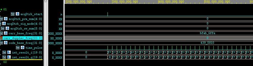
ICMSOA 2020                                                                                                     IOP Publishing
Journal of Physics: Conference Series                         1735 (2021) 012010          doi:10.1088/1742-6596/1735/1/012010

Software and hardware co-simulation verification platform
for navigation SoC

                     Dan Qi*, Mo Chen, Shaozhen Zhang, Dan Cheng and Jun Mu
                     Space Star Technology Co, Ltd, Beijing, China
                     *
                      Corresponding author’s e-mail: qid@spacestar.com.cn
                     Abstract. This paper proposes a software and hardware co-simulation verification platform
                     suitable for satellite navigation SoC chips. The specific implementation scheme is described,
                     and the final simulation results are given. Software simulation is written in c and assembly
                     language, using a complete software compilation and debugging tool chain, hardware
                     simulation is built based on verification methodology, SoC design code is written by verilog,
                     and the software and hardware are coordinated through the VCS compiler to achieve
                     information interaction, and then a universal simulation platform with fast speed, high
                     authenticity and convenient debugging is realized. The simulation results show that the
                     navigation SoC chip functions correctly.

1. Introduction
With the development of our country's Beidou satellite navigation system (BDS), independent design
of application-specific integrated circuits (ASIC) can effectively improve system integration, improve
performance, and reduce power consumption[1], which is more important for achieving national
production and independent control of the navigation industry. It is of great significance, and the
research and development of satellite navigation chips is an important part of the development of
satellite navigation in our country[2].
    In recent years, with the vigorous development of System on Chip (System on Chip) technology,
the development of receiver chips for global navigation satellite systems is of great significance for
improving system integration, improving receiver performance, and reducing receiver power
consumption[3,4]. In the process of chip R&D, in addition to chip design, extensive and
comprehensive verification work is also necessary. Industrial practice shows that verification work in
the SoC design process has accounted for 70% of the total design cycle time, even as high as 85%. The
workload and difficulty have exceeded chip design and become the bottleneck of SoC design and
development[5], and simulation verification is a crucial link in verification work[6].
    This paper proposes a software and hardware co-simulation verification platform suitable for
satellite navigation SoC chips. The software environment and hardware environment construction
methods are described respectively, and also the method of software and hardware information
interacting. Through the navigation signal GPS L1c/a acquisition and tracking function, the simulation
verifies the correctness of the platform and chip functions.

2. Architecture of Navigation SoC
The architecture of the navigation SoC chip is shown in Fig 1. The processor uses ARM926EJ-S and
integrates two 16KB caches as instruction cache and data cache. At the same time, ARM integrates the
VFP9-S coprocessor, which can accelerate the floating-point computing power of the processor, and
can greatly improve the running speed of the program for floating-point computing applications. The

              Content from this work may be used under the terms of the Creative Commons Attribution 3.0 licence. Any further distribution
              of this work must maintain attribution to the author(s) and the title of the work, journal citation and DOI.
Published under licence by IOP Publishing Ltd                          1
ICMSOA 2020                                                                                   IOP Publishing
Journal of Physics: Conference Series            1735 (2021) 012010     doi:10.1088/1742-6596/1735/1/012010

processor integrates a debugging interface and connects to the outside of the chip through the JTAG
interface to provide an online debugging mode. The bus adopts a multi-layer AHB bus, which can
effectively reduce the complexity of a single-layer bus while improving the bus throughput and
response speed, and improve the timing of the bus to support higher bus frequencies.

                                Figure 1. Architecture of navigation SoC.
     AHB bus peripherals include: bootloader ROM, instruction IRAM, data DRAM, VIC interrupt
controller, EBI external bus interface, AHB to APB bridge, AHB to localbus bridge.
    APB peripheral modules include: Timer, Uart, GPIO, SPI, SPF, I2C, WatchDog and CAN bus
interfaces.
    The baseband is the core part of the chip, which realizes the acquisition, tracking, synchronization,
and decoding of navigation signals.

3. Software and Hardware Co-simulation Verification Platform for Navigation SoC
The simulation platform is composed of three parts: simulator, software simulation environment and
hardware simulation environment. Its structural block diagram is shown in Fig 2. Among them, the
simulator refers to the vcs simulation software and its operating platform. The software simulation
environment mainly includes user programs, and the hardware environment mainly includes design
files, intermediate frequency simulation signals, and components such as driver and monitor. The chip
design file is the test target of the simulation platform, and the user program and the intermediate
frequency simulation signal are the test vectors of the simulation platform. The chip RTL code is used
for pre-simulation, and the chip netlist file is used for post-simulation.
    In order to reduce the simulation time as much as possible, the verification work of the chip boot
unit is verified by some special test cases, so the verification work of the platform no longer involves
the boot unit. In addition, the navigation SoC contains a variety of different types of interfaces, which
need to be simulated and verified. The simulation in this article does not involve interfaces, and
mainly takes baseband GPS L1c/a acquisition and tracking as an example.

                                                       2
ICMSOA 2020 IOP Publishing
Journal of Physics: Conference Series 1735 (2021) 012010 doi:10.1088/1742-6596/1735/1/012010
Figure 2. Software and hardware co-simulation verification platform.
3.1. Software environment
The user program of the software simulation environment is written by a mixture of c and assembly
language. Through software compiler, assembler, linker and other tools, the software program is
converted into an executable image file through the use of makefile scripts, and then the file
conversion tool fromelf. The image file is converted into a binary mif file and loaded into the SoC chip
memory. When the chip boot starts, the ARM core calls the software code and executes the program.
The structure of the software code is shown in Fig 3. After the system BOOT is up, it directly
jumps to the main() function for single-process tasks. If an interrupt exception occurs, the boot code
jumps to the interrupt handling function according to the interrupt vector table address. The interrupt
3ICMSOA 2020 IOP Publishing
Journal of Physics: Conference Series 1735 (2021) 012010 doi:10.1088/1742-6596/1735/1/012010
processing function includes the processing of each interrupt. The main() function calls the TC (Test
Case) function of each module, and TC calls the underlying driver code. The writing of the driver code
is based on the register definition files and global variables of each module. The software structure is
clear and controllable, which is convenient for the parallel submission and management of test cases.
Figure 3. The structure of the software code.
Since the simulation user program is the most core part of the test vector, it directly determines
the simulation duration, so its design should be as simple as possible on the basis of covering the
navigation SoC functions. The simulation user program flow is as follows:
①Set the baseband clock and reset in the main function.
②Put the acquisition parameters into the main function and start the signal acquisition program.
③Put the tracking parameters into the main function, and start the corresponding tracking channel
program.
④Timely detect the acquisition completion flag. If the acquisition completion flag is detected, it
indicates that the acquisition unit has completed the signal acquisition.
⑤Regularly detect the track channel status, bit synchronization status, switch tracking parameters,
etc.
⑥ In the main function, read the acquisition results, tracking status, related integration results and
channel observations.
3.2. Hardware environment
The intermediate frequency simulation signal of the hardware simulation environment is generated by
the Matlab program. Based on the UVM verification methodology, the driver component is used to
input the IF signal to the ad data interface, and the monitor component is used to observe the
acquisition successful signal, and output the tracking integral value to a text file. The result analysis of
the chip is divided into two ways, one is to use the waveform file to observe the simulation details, and
the other is to use the Matlab software to perform data analysis and chart drawing on the output text
file. Taking GPS L1c/a as an example, the information of the simulated input intermediate frequency
sampling signal is shown in Table 1.
4ICMSOA 2020 IOP Publishing
Journal of Physics: Conference Series 1735 (2021) 012010 doi:10.1088/1742-6596/1735/1/012010
Table 1. The information of the IF signal.
Satellite Signal Satellite IF Doppler Initial code Sample Carrier to noise
system number (MHz) frequency phase frequency ratio
(Hz) (chip) (MHz) (db﹒Hz)
GPS L1c/a 1 46.42 0 0 62 44
4. Simulation Results and Discussion
By executing the user program, the simulation platform can display the control flow and data flow of
the navigation SoC in the user program operation, AHB bus timing, satellite signal acquisition,
channel tracking and other key modules. Using the acquisition results, related integral values and
channel state observations output by the interface, it can be judged whether each functional module is
operating normally. Based on the above simulation platform architecture, the simulation of the satellite
navigation baseband SoC is completed by using vcs, integrated development environment, and Matlab
software. The simulation result is shown in Fig 4, where acq2trk_start represents the successful
acquisition flag, int_result_i, int_result_q are the tracking integral values, and the tracking integral
value is analyzed by Matlab as shown in Fig 5. The simulation results show that the baseband
acquisition and tracking function of the navigation SoC is normal.
Figure 4. The simulation result.
Figure 5. The analyzed result by matlab.
5ICMSOA 2020 IOP Publishing
Journal of Physics: Conference Series 1735 (2021) 012010 doi:10.1088/1742-6596/1735/1/012010
5. Conclusion
This article introduces a software and hardware co-simulation verification platform for satellite
navigation SoCs, elaborates the specific implementation scheme, and gives the final simulation results.
The pre-simulation and post-simulation are performed through the design simulation verification
platform. The chip design files and application software are organically combined during the
simulation process to display the control flow and data flow of the satellite navigation SoC during the
program operation, and verify the correctness of the key modules , which effectively improves the
success rate of chip design and ensures that the chip can be successfully taped out once.
Acknowledgments
I would like to express my gratitude to all those who helped me during the writing of this paper.
Thanks for the excellent development platform and financial support provided by the IC Design
Center in Space Star Technology Co. Ltd. Special thanks to all members of the navigation SOC project.
References
[1] Wang Bisheng, Lu Shanwei, Yang Dongkai, Zhang Qishan. A New Solution to GNSS Receiver
Baseband Signal Processing SoC Platform Based on Open RISC Processor[C], 7th International
Conference on Wireless Communications, Networking and Mobile Computing(WiCOM), 2011: 1-4.
[2] Zhang Rong, Huang Haiying, Li Chunzhi. Software and Hardware Design of the Embedded
Test System Based on NIOSII Soft-core Processor[J]. Computer Measurement & Control, 2012, 20(2):
303-306.
[3] Xie Gang. Principles of GPS and Receiver Design[M]. Beijing: Publishing House of Electronics
Industry, 2009: 5.
[4] Zhao Gang, Hou Ligang, Liu Yuan, Zhu Xiudian, Wu Wuchen. Methodology of SoC Design
Using Hardware/Software Co-simulation[J]. Microelectronic & Computer, 2006, 23(6): 247-249.
[5] Yan Chao. Research of GPS Baseband SoC Design and Key Technology[D]. Chongqing:
Chongqing University, 2014.
[6] Liao Mengxin. Research and Implementation of Design and Verification Platform for
Navigation Receiver SOC[D].Shanghai: Shanghai Jiao Tong University, 2011.
6You can also read