THE AUSTRALIAN NATIONAL FABRICATION FACILITY ENABLED BY ANFF 2020 - ANFF.ORG.AU
←
→
Page content transcription
If your browser does not render page correctly, please read the page content below

THE AUSTRALIAN
NATIONAL
FABRICATION
FACILITY

    ENABLED
    BY ANFF
      2020

                 ANFF.ORG.AU
ENABLED BY ANFF

The production of the 2020 Casebook comes amid the                 As I complete my first year as CEO of ANFF I reflect on how
turmoil of the COVID 19 pandemic, a time that has                  much has changed so quickly. In late 2019 the executive
seen the importance of research, development, and                  team started to review and refresh the organisation’s
commercialisation of technologies thrust to the fore.              strategy documents. The focus was around maintaining
                                                                   our research infrastructure excellence and starting to
The creation of new revenue streams and businesses                 consider how best to support the vast amount of industry
based on new technologies, novel manufacturing and                 engagement and commercialisation activity that is based
new employment have rightly become central pillars of              on the use of our tools.
the Commonwealth Government’s strategy for economic
recovery.                                                          When COVID 19 caused lockdowns and the Nation’s supply
                                                                   lines became stressed or inactive, ANFF pitched in and
These activities place ANFF, our NCRIS colleagues, and our         excelled to the best of our abilities. We manufactured, tested
clients at the heart of Australia’s innovative future, and we      and supplied personal protective equipment items for front
stand ready to enable the Nation to capture the benefits           line workers at no cost. We accelerated a number of projects
of its investments in research at all levels of technology         that have relevance to infectious diseases by significantly
readiness.                                                         reducing cost and lending all of our engineering talent and
However, it’s only through sustained support that                  tools to the cause. I would like to thank NCRIS and the
organisations such as ANFF can be ready to provide the             Department of Education, Skills and Employment (DESE) for
flexible capability required to secure Australia’s future. As      supporting ANFF and the new mode of operating. I would
such, the Board of ANFF thanks NCRIS for its continued             also like to thank all the ANFF staff members that went
support and funding, and expresses enormous appreciation           above and beyond to help when the Nation needed it most.
to the institutions that have housed ANFF facilities and           As supply lines reopen and lockdown restrictions ease, we
provided matching funds to enable the purchase of cutting-         have moved back to normal operations but in a new era
edge equipment.                                                    – this era has a new energy for sovereign capability and
Due to this support ANFF has been able to pivot to provide         rebooting the Australian Economy. A new focus for ANFF
for emerging needs, and our ability to do so has been              strategy became clear.
demonstrated throughout the COVID crisis. ANFF Nodes               We need to use our tools and talent to directly support
have continued to offer safe services with experienced             research and research translation in industry sectors
technologists providing clients with outcomes and training.        that we already have a good track record. These are
ANFF’s strong backing of COVID-related projects has seen us        additional efforts that will add to our core remit of providing
assist Australia’s immediate response, and the realisation of      Australian innovators with access to world-class research
new research.                                                      infrastructure, but we are going to be both proactive and
Despite COVID, the past year has seen the almost 3,000             aggressive in putting added focus into the areas that we
users of ANFF facilities produce a steady stream of high-          can do the most good – Healthcare and Biotech, Space and
quality science and engineering that has enabled Australia         Defence and Renewable Energy.
to claim world leadership in a number of areas. Some are           We will augment the ANFF team to facilitate this focus
described in this Casebook which I strongly commend to             and also to better integrate with other industry groups and
you, and I speak for the Board when I thank all of those           strategic partners. We will also be keeping a close eye on
associated with the Facility for their substantial contributions   promising home-grown technology that would benefit from
in recent years and the many users of ANFF for their               additional support. As such ANFF and its University partners
presentation of so many interesting fabrication challenges.        can together nurture these emerging technologies and
                                                                   companies through the valley of death. It’s a role that ANFF
While the future seems turbulent, the appointment of our
                                                                   is in a unique position to play.
new CEO, Dr Ian Griffiths positions us to provide calm and
efficient assistance to our clients as they travel the many        As you will see in the ANFF Casebook we’re doing some
paths towards commercialisation. We therefore look ahead           incredible things and as we move forward we will continue
with excitement and resolve as we continue to enable the           to add value to the Nation. Now is an exciting time to be
research that will allow Australia to thrive.                      in ANFF.
Emeritus Professor Chris Fell AM FTSE HonFIEA ust CPEng            Dr Ian Griffiths
ANFF Chairman                                                      ANFF CEO

2
CONTENTS
         This Casebook features stories split into three sections: Excellence in research;
       Capturing the Benefit; and Establishing industries. Flagship Focus pages take a look
          at some of the most unique capabilities available through the ANFF network.

                                                                      02 Welcome
    Snapshot of ANFF 04

                                                                      05 ANFF in numbers
Excellence in research 06
                                                                      10 ANFF-VIC
              ANFF-Q 15
                                                                      18 Optofab Node
 Capturing the benefit 20

                                                                      25 ANFF-NSW
           ANFF-ACT 29

                                                                      32 ANFF-SA
Establishing industries 34
                                                                      39 Materials Node
 Access/contact ANFF 46

                                                                         Australian National
                                                                         Fabrication Facility Ltd
                                                                         151 Wellington Road
                                                                         Clayton VIC 3168
                                                                         T: +61 3 9902 9619
                                                                         E: info@anff.org.au
                                                                         www.anff.org.au

                                                                                                    3
SNAPSHOT
                               OF ANFF
    ANFF was established under        ANFF’s mission is to provide         Over 500 tools are located across
    the Australian Government’s   micro and nano fabrication facilities     21 institutions around Australia
       National Collaborative      for Australia’s researchers, SMEs       in a national network of 8 Nodes.
      Research Infrastructure           and start-up companies.            Each Node offers complementary
         Strategy (NCRIS).                                                specialised manufacturing facilities
                                                                               supported by trained staff.

                                  THE 8 NODES OF ANFF
                                           NODE         HUB
                                                                                                       QLD
                                                                                                      NODE

       WA                                                                                                OPTOFAB
      NODE                                                                                                NODE
                                                                                                  NSW
                                                                                                  NODE
                                                           SA
                                                          NODE
                                                                                         MATERIALS
                                                                                     ACT  NODE
                                                                     VIC            NODE
                                                                    NODE

4
ANFF IN
                        NUMBERS
FY2020 was yet another strong year for ANFF, here’s a few of the stand out statistics.

        2,936                                       20+ years
   clients helped – average time                     ANFF tools were being used for
       on equipment per user                      a total of 178,162 hours, equivalent
         exceeded 60 hours                               to more than 20 years

      +$50m                                                   808
  Funding injected into ANFF by                   ANFF was acknowledged more than
Federal and State Governments as                   808 times in publications in 2019
 well as our Member Institutions

      2,500+                                                  130
 More than 2,500 on-tool training              There are now 130 ANFF experts to assist
    sessions were conducted                      the Australian research community

                                                                                          5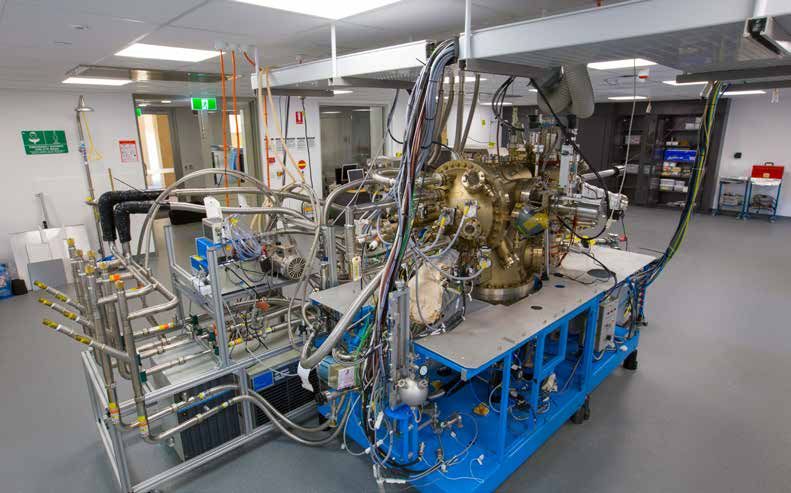
EXCELLENCE IN RESEARCH
ANFF’s equipment and expertise enables research excellence, we do this by making cutting-edge
capability suites, world-class engineers, and supporting infrastructure available to all.
Ensuring our capabilities are world-leading allows us to support early stage research projects that
provide the foundations of future products, jobs, and businesses, as well as providing immediate
benefits to Australia, economically or otherwise.
This section of the Casebook presents a small sample of the hundreds of projects that ANFF helps
on a yearly basis that exhibit excellence in research.
SUPERPOWERED
STITCHES
Medical sutures could provide a conduit to deliver
anti-inflammatory treatments directly into damaged
tissue. Recent research has demonstrated that drugs can
be drawn along the threads of the stitches themselves
before being widely dispersed into soft tissue models.

This enticing approach to targeted wound treatment has recently           The researchers use the electrophoresis phenomenon to drive
been trialled by researchers from the ARC Centre of Excellence            bioactive molecules rapidly along the thread towards the desired
for Electromaterials Science (ACES) utilising electricity, standard       distribution area by placing electrodes at either end of the
sutures, anti-inflammatory medicines and a hydrogel testbed.              suture and passing a small current through it. Once within the
                                                                          target tissue, the current is dropped, causing the flow to slow
The team, led by Professor Brett Paull and including scientists
                                                                          and allowing uptake of the drug into the biological model. Once
from ACES’ University of Tasmania (UTAS) and University of
                                                                          the required time has passed, the current is ramped up again to
Wollongong (UOW) sites, has shown that their electrofluidic
                                                                          sweep out the remaining bioactive and potentially any resultant
method allowed the drug to spread across the full 3D space
                                                                          cell metabolites of interest.
of the testbed, and after two hours of electrical stimulation,
over 80 per cent of the drug was retained within the target area.         “The fascinating aspect of this work lies within its simplicity,”
                                                                          Professor Paull said. “We can actually be highly quantitative in
To provide effective delivery of treatment in this way, medicine
                                                                          delivery of these bioactive species using some very simple materials,
needs to travel quickly along the suture, but then slow down once it
                                                                          and not only deliver from A to B, but anywhere in-between”
arrives in the target tissue to allow uptake of the drug into the body.
                                                                          “Our work, supported by ANFF Materials, showed that more than
Professor Paull and his colleagues have shown that their
                                                                          80 per cent of the anti-inflammatory stayed within the hydrogel,
electrofluidic approach enables them to vary the speed that
                                                                          and therefore indicates distinct promise for use in real tissue.
bioactive molecules are carried along a typical absorbable suture
                                                                          We look forward to taking this research further.”
by employing an electric field to manipulate the medicine.
Most water-soluble species carry some sort of charge and will
therefore migrate towards either positive or negative electrodes
when exposed to an electric current.
The principle of driving medicine along a fibre using a current in
this way has been demonstrated previously, but it’s never been
tested in a biological model. To see if the approach could work in
the wild, the ACES researchers turned to ANFF Materials experts
to create a testbed tissue using a hydrogel called GelMA.
GelMA is a fantastic replica of natural tissue – it’s made of
denatured collagen, a protein vital to building connective tissue
within the body, and can be cured to varying degrees by
exposing it to different amounts of UV light to produce different
mechanical properties.
Using this highly accurate model allowed the researchers to
investigate aspects of how the delivery approach could work
with live cell cultures.

                                                               ELECTROFLUIDICS CAN
                                                               ALLOW FOR STRATEGIC
                                                               DISTRIBUTION OF ANTI-
                                                               INFLAMMATORY DRUGS.
                                                               Credit: Brett Paull

                                                                                                                                          7
NOVEL DEVICE
DETECTS PRE-ECLAMPSIA
BIOMARKERS
Australian researchers are prototyping an affordable device
capable of diagnosing pre-eclampsia within half an hour.

Approximately 76,000 pregnant women and 500,000 babies             The sensor works by placing a droplet of the patient’s blood
die from pre-eclampsia across the world every year. Women in       onto a sensitive area of the device. This area contains receptors
developing countries are seven times more likely to suffer from    specific to pre-eclampsia biomarkers – if present, the biomarkers
the condition due to delayed diagnosis and a lack of access to     bind to the receptors and change the flow of electricity across
hospitals.                                                         the device. By monitoring these fluctuations in current, the
                                                                   presence and approximate quantity of pre-eclampsia biomarkers
Causes of pre-eclampsia are not entirely understood, but if left
                                                                   can be confirmed, allowing doctors to quickly react and mitigate
untreated it can lead to blood clots, organ failure, and death.
                                                                   the potentially life-threatening symptoms. Because the level of
Rapid, affordable, and accurate diagnostic tools are therefore
                                                                   biomarkers can be detected, the severity of the condition can
essential in aiding treatment.
                                                                   also be determined.
Now, a hand-held diagnostic device being developed by Professor
                                                                   With support from the ARC Centre for Bio-Nano Science (CBNS),
Benjamin Thierry, Dr Duy Tran and a team from the University
                                                                   Dr Tran has built on local expertise to integrate his sensing
of South Australia’s Future Industries Institute (UniSA FII) has
                                                                   technology within cost-effective and easy-to-operate diagnostic
shown it could pose a solution.
                                                                   devices that can be operated with minimal training by nurses
The affordable technology is already showing promising signs       and other primary healthcare providers in regional and remote
during early testing – a prototype developed by Dr Tran and PhD    communities, both here in Australia and worldwide.
student Ms Thuy Pham has been successfully validated on four
                                                                   The next generation of the device is currently being developed
women with confirmed pre-eclampsia, and there are plans for
                                                                   with the support of the Medical Device Partnership Program
further trials to be conducted in the Royal Womens Hospital
                                                                   (MDPP) as a handheld analyser unit with single-use disposable
(Melbourne) and Vietnam in the near future.
                                                                   sensing cartridges, anticipated to be manufactured for as little as
The team’s new tool utilises a sensor developed at ANFF-           two dollars.
SA, where Dr Tran has been harnessing the Node’s technical
expertise and its lithography and sputtering equipment to
fabricate and fine-tune the device.

                                                                                                    DR DUY TRAN HAS
                                                                                                    BEEN WORKING WITH
                                                                                                    ANFF-SA ON A LIFE
                                                                                                    SAVING DIAGNOSTIC TOOL.
                                                                                                    Credit: Brenton Edwards

  8
ARRAYS OF NANOFABRICATED
                                                                                                           STRUCTURES ENABLE RESEARCHERS TO
                                                                                                           HARNESS
                                                                                                           NOVEL OPTICAL PROPERTIES.
                                                                                                           Credit: TMOS

                                                                     TMOS researchers are developing the devices that are expected
                                                                     to unlock widespread use of holographic displays, artificial vision,
                                                                     wearable medical devices, and ultra-fast WiFi whilst also laying the
                                                                     foundations for many more applications that are yet to be imagined.
                                                                     The aim of TMOS is to develop ultrathin devices that create,
                                                                     manipulate, and detect light. These platforms are part of
                                                                     a movement towards meta-optical components that use
                                                                     nanofabricated structures to control light in ways that go beyond
                                                                     what is achievable by traditional approaches to photonics.
  HV      det   moe   dwell    curr     WD      mag         HFW
5.00 kV   TLD   SE    1 μs    6.3 pA   4.4 mm   25 000 x   8.29 μm
                                                                     The team’s latest ANFF-enabled research, led by the group of
                                                                     Professor Andrey Sukhorukov, drives the development of novel
                                                                     meta-optical devices for quantum applications.

       TMOS
                                                                     The specific design by PhD student Shaun Lang is tailored for
                                                                     manipulation of entangled photons. These paired particles can
                                                                     be used to deliver the potential of quantum computers and to

       LIGHTS
                                                                     transmit unbreakable messages across incredible distances.
                                                                     The entanglement principle is a quantum phenomenon that sees
                                                                     pairs of particles such as photons becoming twinned so that any

       THE WAY
                                                                     changes made to one partnered particle is exhibited by the other.
                                                                     Theoretically, this connection remains regardless of how far apart
                                                                     the particles are, even if they’re separated to opposite sides of
                                                                     the universe.

       Researchers at the ANU-led ARC                                The project shows a way to change the polarisation of two
                                                                     photons simultaneously, which can accordingly modify the
       Centre of Excellence for Transformative                       degree of quantum entanglement, an operation essential for a
                                                                     range of quantum protocols.
       Meta-Optical Systems (TMOS) are
                                                                     The research demonstrates a use of an array of structures called
       producing the light-based technologies                        nanoresonators, which are features that measure 100 times
       that are needed to meet the evolving                          smaller than a human hair. They resonate differently depending
                                                                     on the incoming light polarisation across a particular range of
       demands of Industry 4.0.                                      wavelengths.
                                                                     Importantly, the optimisation of the arrangement and dimensions
                                                                     of the individual nanoresonators, which in combination form
                                                                     an ultrathin metasurface, allows the implementation of multiple
                                                                     controllable transformations of photon polarisations with a
                                                                     single device.
                                                                     The metasurfaces were fabricated at ANFF-ACT using electron
                                                                     beam lithography and inductively coupled plasma etching,
                                                                     creating silicon nanostructure arrays with a thickness of 800
                                                                     nm, optimised for operation around the 1,550 nm wavelength
                                                                     range which is compatible with the telecommunications industry.
                                                                     “The advanced equipment and dedicated staff at ANFF enable
                                                                     the fabrication with remarkable quality down to nanoscale,”
                                                                     said Dr Jihua Zhang, a postdoctoral fellow working on quantum
                                                                     metasurfaces.
                                                                     “This topic is an important part of the research mission in TMOS.
                                                                     Through ANFF-ACT and other sister nodes, we aim to develop the
                                                                     science and technology of meta-optics into novel devices and
                                                                     translate them into practical applications such as holographic
                                                                     displays, wearable optical sensors, remote sensing and imaging,”
                                                                     said Prof. Dragomir Neshev, director of TMOS.
                                                                                                                                     9
FLAGSHIP
          FOCUS

Victoria's network of nanofab
ANFF-VIC ties the largest open-access cleanroom in the southern hemisphere
with six university-based hubs spread across Victoria providing a full complement
of nanofabrication capabilities and expertise.

The Node spans the University of Melbourne; Deakin University;       well-being and understanding disease. LIMS involves a broad
La Trobe University; Swinburne University of Technology; Victoria    collaboration of scientists that addresses key problems which
University; RMIT University; the CSIRO; and the unique Melbourne     will significantly benefit Australian society. Cross-disciplinary
Centre for Nanofabrication (MCN), which is hosted by Monash          collaborations, high-impact innovations, and commercialisation
University.                                                          will be strongly supported by this new MCN equipment.
MCN is home to ANFF’s national headquarters. The ISO9001-            The new tool will form part of the process chain for key
certified Centre is a world-class, purpose-built facility boasting   technologies being developed by LIMS allowing them to establish
state-of-the-art cleanrooms (class 10,000 and class 100), and        pilot production at the MCN.
reconfigurable biochemistry, microscopy and PC2 labs. These
specialised work environments house top-of-the-line micro            The next-level Nanofrazor
and nanofabrication equipment and precision measurement              The MCN is home to Australia’s first (and only) Nanofrazor, a
instrumentation.                                                     lithography tool which is the result of more than 20 years of
                                                                     intensive research and development that started at IBM Research
Imminent arrival of the fabled Phabler                               in Zurich and has been extended at the spin-out, SwissLitho.
The latest flagship tool to be added to the MCN’s suite of world-
                                                                     The Nanofrazor instrument performs t-SPL, a 3D direct-write
class capabilities is the Phabler 150, manufactured by Eulitha,
                                                                     lithography technique that provides sub-10 nm lateral resolution
which provides unprecedented ability to print high-resolution
                                                                     with sub-2 nm vertical accuracy, all under ambient temperature
periodic nanostructures in a low-cost photolithography system.
                                                                     and pressure conditions.
The Phabler is similar to a conventional mask-aligner where
                                                                     During patterning, a 1,000°C+ cantilevered tip made of doped
a photoresist coated wafer is put in proximity to a mask and
                                                                     silicon scans over the surface of a sample, and in so doing
exposed by a beam of UV light, but thanks to the manufacturer’s
                                                                     sublimates a polymer resist known as PPA leaving nanoscopic
breakthrough PHABLE exposure technology, the resolution is no
                                                                     topologies in its wake. As a secondary benefit to the AFM-based
longer limited by diffraction.
                                                                     technology the Nanofrazor is capable of acting as an AFM as
Through a collaboration with La Trobe University, MCN has            well, enabling real-time feedback control of the writing process.
secured this tool to address a substantial need for rapid high-
                                                                     The process isn’t reliant on an ion gun or electron beam, which
resolution, large area patterning techniques. This need is arising
                                                                     is helpful when dealing with sensitive electronic materials. It
due to advances in the field of 2D metamaterials with related
                                                                     operates at ambient temperature, pressure, low voltage, and
applications in diverse areas such as bio-sensing, nanophotonics,
                                                                     under nitrogen atmosphere sidestepping the need for a costly
plasmonics, nanomagnetism, and more.
                                                                     and cumbersome high-vacuum environment.
Acquisition of the Phabler has been driven by research being
                                                                     The ease of use and high resolution means it is ideal for rapid
conducted at the La Trobe Institute for Molecular Sciences
                                                                     fabrication of three-dimensional nanostructures needed to
(LIMS). The institute is focused on the development, translation,
                                                                     create novel proof of concept devices and components for
and commercialisation of technology with a focus on health and
                                                                     nanophotonics, nanooptics, nanoelectronics, and plasmonics
                                                                     applications.
  10
AROUND THE NODE +
Fab Fibres at Deakin’s IFM Gain a deeper understanding at La Trobe
At Deakin’s Institute of Frontier Materials (IFM), ANFF-VIC ANFF-VIC’s La Trobe hub housed within the Centre for Material
provides access to a fibre processing line that allows researchers Surface Science provides access to time-of-flight secondary-ion
and engineers to produce or enhance the functionality of novel mass spectrometry (ToF-SIMS) analysis.
fibres. The fibre production suite includes melt extrusion, wet
ToF-SIMS is a microprobe technique and can produce mass
spinning, and fibre coating capabilities that range in size from
spectra from points or areas on a sample surface, molecular
small-scale benchtop to pilot-scale experiments, and are able to
maps (2D) and depth profiles. The process provides detailed
spin or coat a diverse range of synthetic and natural polymers
information about the molecular composition of a surface,
with additives such as nanomaterials.
including isotope information and molecular weight.
Harnessing this equipment enables outcomes such as work
During a ToF-SIMS experiment, the sample is bombarded with
published by scientists from Drexel University and Deakin in
a focused beam of high-energy ions which fragments material
March 2020 that demonstrated a new knitted supercapacitor
from the outer nanoscopic layers of a sample’s surface. Some
architecture to enable wearable energy storage devices. The
of these ejected fragments are ionised, and these so-called
international team worked with ANFF experts to develop a
secondary ions are then analysed. The material emitted from
method to fabricate large quantities of conductive fibres that
the surface is passed through an electrostatic field, which
could be used to produce energy storing textiles to power devices
uniformly accelerates all ionised particles towards a detector.
such as flexible electronic components and smart garments.
Particles with different masses but the same energy will take
ANFF’s equipment at the IFM was used to perfect and automate different amounts of time to reach the detector, and it’s by
the fabrication process. Melt extrusion was used to produce studying this time of flight that the ion’s mass can be deduced,
a nylon fibre and the wet spinning line used to coat the nylon leading to the identification of what chemical it is.
in a promising 2D nanomaterial (MXene) adding capacitive
functionality, which were then knitted into supercapacitors. Interfacing at RMIT
Within RMIT’s Micro Nano Research Facility (MNRF) is a host
Surface coatings covered at Swinburne of fabrication equipment with a particular focus on interfacing
Swinburne University’s Biointerface Engineering Hub is home to micro and nanotechnologies to the macro world.
an array of polymer surface coating and surface analysis tools,
The MNRF team provide access to a multi-functional 3D printer
including plasma polymerisation, dip coating and more.
capability of printing polymers, ceramics and metals. This builds on
The Hub houses six custom made reactors for plasma and complements the Low-temperature co-fired ceramic (LTCC)
polymerisation (PECVD) and plasma treatment. PECVD produces facility at RMIT to enable rapid prototyping of sophisticated
thin films by fragmenting a selected molecule with a plasma integrated ceramic packages for electronics, photonics, MEMS
and coating everything inside the reactor with it including the for extreme conditions, and biomedical implantation.
desired surface. It’s possible to vary the chemistry of the film by
The suite of capabilities provides robust, compact, but
changing the conditions within the reactor, and the thickness of
highly flexible packaging so that ANFF users can ready their
the film can also be changed by controlling the deposition time.
technologies for real world contexts such as standardised
The process is substrate independent, and deposits pinhole-free electronic, photonic, and fluidic interfaces.
thin films in the range ofPERSONALISING
NUTRITION
A wearable smart patch could deliver precision data to help
people personalise their diets and reduce their risk of developing
lifestyle-related chronic diseases like Type 2 diabetes.
The world-first personalised nutrition wearable being developed Professor Sriram said RMIT researchers would integrate the
by Melbourne-based start-up Nutromics is designed to measure technologies in a prototype smart patch that could be cost-
dietary biomarkers and send the information to an app, enabling efficiently manufactured, and was designed with the end-user
users to precisely track how their bodies respond to different foods. at front of mind. “This smart patch is a significant evolution in
wearable health monitoring technology,” he said.
The pioneering technology will be designed and manufactured
in Australia. Professor Nam-Trung Nguyen, Director of the Queensland Micro-
and Nanotechnology Centre at Griffith University and Deputy
A collaborative team led by Nutromics, Griffith University, RMIT
Director of ANFF-Q, said the project was underpinned by the
and manufacturer Romar Engineering, with support from the
centre’s past and ongoing fundamental research in microfluidics
Innovative Manufacturing Cooperative Research Centre (IMCRC),
and wearable, implantable microsystems.
is now researching and developing the required manufacturing
capabilities to pilot manufacture the device. “One of the research pillars at the Queensland Micro- and
Nanotechnology Centre is that we move towards the
Pre-diabetes is estimated to affect more than 350 million people
commercialisation and translation of our discoveries for the
globally; in the US and China alone, 1 in 2 adults are pre-diabetic
benefit of end users,’’ he said.
or diabetic.
“The project will benefit significantly from the recent addition
Nutromics co-CEO Peter Vranes said the smart patch leveraged
of a femto second laser machining system funded by the ARC.”
emerging technologies to empower people to take greater
control of their health. Alan Lipman, CEO of Romar Engineering, an established
manufacturer of medical devices, said collaboration was the way
“Being able to easily monitor key dietary biomarkers will give you
forward for Australian manufacturing.
the knowledge to personalise your diet to suit your own body, to
get healthy and stay healthy,” Vranes said. “Working with entrepreneurs, academics and researchers to
develop new medical technologies is essential to maintain
Diabetes is one of the largest chronic health challenges globally.
Australia’s international competitiveness and to build a strong
Without taking any action, up to 70% of people with pre-diabetes
domestic manufacturing skills base.”
can go on to develop Type 2 diabetes within the next four years,
but with early interventions and lifestyle changes, the condition
THIS STORY WAS ORIGINALLY PUBLISHED BY GRIFFITH
is largely preventable.
UNIVERSITY, FIND OUT MORE AT: NEWS.GRIFFITH.EDU.AU
The fabrication of sample collection will be led by Griffith
University and Romar Engineering, with sensor integration and
stretchable electronics fabrication undertaken at RMIT’s Micro
Nano Research Facility, an intrinsic hub of ANFF’s Victorian Node.
Research Co-Director of RMIT’s Functional Materials and
Microsystems Research Group, Professor Sharath Sriram, said
the smart patch combined a complex sensing platform and
stretchable electronics for improved conformity to skin.
AN ARRAY OF NEEDLES THAT COULD
BE USED TO PROVIDE PERSONALISED
DIETARY GUIDANCE, PRINTED USING
ANFF-Q’S NANOSCRIBE.
Credit: Nam-Trung Nguyen
12DANCING HELIUM
University of Queensland researchers are using a fluid
that never settles to create quantum tornadoes on a chip.
The team, led by Professor Warwick Bowen has been working This result can be harnessed to create ultraprecise sensors,
to understand and harness interactions between waves in ultranarrow light filters, low power devices, precision silicon chips,
superfluid helium and light. Their research leads on to new and more. Due to the forces at play, they are less susceptible to
light-based technologies that require very little energy and are shock and vibration than their MEMS-based equivalents, and they
hypersensitive, while at the same time providing an insight into could also have performance benefits.
turbulent systems such as cyclones and interstellar objects.
Another bizarre behaviour of quantum liquids is that they can
Professor Bowen’s research is centred on a raised silicon disk only carry integer circulation, which means they can only flow
that was nanofabricated with help from ANFF-Q equipment and at fixed velocities. They can therefore be used to provide an
expertise. The structure’s shape traps light at its edges, creating absolute reference frame for acceleration measurement. This
a cavity that can keep photons circling for a limited time. would allow a system to track its position without the need for
satellites, making location pinpointing in submarines, in-door
This disk is then coated with superfluid helium – this is an
shopping centres, and underground far more accurate.
approach unique to Professor Bowen’s laboratory and the work
builds on the team’s previous endeavours that showed laser There’s yet more novel effects to unlock however – Professor
cooling can be used to sustain the temperatures required to keep Bowen’s devices can stir the superfluid helium to trigger
the helium film in this superfluid state. vortices that will go on forever, and this provides a significant
opportunities as a method to study turbulence. Professor
Superfluids are quantum liquids that are characterised by the
Bowen said it was postulated more than 50 years ago that the
fact that they have no viscosity, and flow without losing any
turbulence problem could be simplified using quantum liquids.
energy. This means if a wave or a vortex starts in the superfluid,
it won’t ever stop of its own accord. In Professor Bowen’s device, “Our new technique is exciting because it allows quantum
a superfluid acoustic wave is triggered to flow around the disks turbulence, which mirrors the sort of behaviour you see in
edge, travelling in the exact same space as the trapped light. cyclones, to be studied on a silicon chip for the first time,”
Professor Bowen said. The research also had implications in
This colocation leads to the light interacting with the acoustic
space, where quantum liquids are predicted to exist within dense
wave, which triggers a phenomenon called Brillouin scattering.
astrophysical objects.
The effect causes the light particles to be absorbed and re-
emitted with lower energy. The energy difference is taken up “Our finding allows us to observe this nanoscale quantum
by the acoustic wave, amplifying it. The result is in effect an turbulence in the lab, and this research could help to explain how
incredibly low power, and low threshold type of laser for sound, these objects behave,” he said.
rather than light.
13LIGHT, FANTASTIC:
THE PATH AHEAD FOR FASTER,
SMALLER COMPUTER PROCESSORS
Australian and German physicists have developed a hybrid
architecture to overcome some of the engineering hurdles
that are slowing the uptake of light-based computing.
Light is emerging as the leading vehicle for information “This sort of efficiency and miniaturisation will be essential in
processing and telecommunications as our need for energy transforming computer processing to be based on light. It will
efficiency and bandwidth increases – developing affordable and also be very useful in the development of quantum-optical
scalable photonic chips is therefore essential. information systems, a promising platform for future quantum
computers,” said Associate Professor Stefano Palomba, a co-
However, there remain substantial engineering barriers to
author from the University of Sydney and Nanophotonics Leader
complete this transformation. Industry-standard silicon circuits
at Sydney Nano.
that support light are more than an order of magnitude larger
than modern electronic transistors. One solution is to ‘compress’ “Eventually we expect photonic information will migrate to
light using metallic waveguides – however this would not the CPU, the heart of any modern computer. Such a vision has
only require a new manufacturing infrastructure, but also the already been mapped out by IBM.”
way light interacts with metals on chips means that photonic
On-chip nanometre-scale devices that use metals (known as
information is easily lost.
“plasmonic” devices) allow for functionality that no conventional
Now scientists in Australia and Germany have developed a photonic device allows. Most notably, they efficiently compress
modular method to design nanoscale devices to help overcome light down to a few billionths of a metre and thus achieve hugely
these problems, combining the best of traditional chip design enhanced, interference-free, light-to-matter interactions.
with photonic architecture in a hybrid structure. Their research
“As well as revolutionising general processing, this is very useful
was in Nature Communications in May 2020.
for specialised scientific processes such as nano-spectroscopy,
“We have built a bridge between industry-standard silicon atomic-scale sensing and nanoscale detectors,” said Dr Tuniz
photonic systems and the metal-based waveguides that can be also from the Sydney Institute of Photonics and Optical Science.
made 100 times smaller while retaining efficiency,” said lead
“We have shown that two separate designs can be joined
author Dr Alessandro Tuniz from the University of Sydney Nano
together to enhance a run-of-the-mill chip that previously did
Institute and School of Physics.
nothing special,” Dr Tuniz said.
This hybrid approach, developed with assistance from ANFF-NSW
This modular approach allows for rapid rotation of light
University of Sydney Hub, allows the manipulation of light at the
polarisation in the chip and, because of that rotation, quickly
nanoscale, measured in billionths of a metre. The scientists have
permits nano-focusing down to about 100 times less than the
shown that they can achieve data manipulation at 100 times
wavelength.
smaller than the wavelength of light carrying the information.
This story was written
by Marcus Strom for the
University of Sydney, originally
titled: Light, fantastic: the
path ahead for faster, smaller
computer processors.
Find out more at
https://bit.ly/3jzYqSj
(FROM LEFT) ASSOCIATE
PROFESSOR STEFANO PALOMBA,
DR ALESSANDRO TUNIZ,
PROFESSOR MARTIJN DE STERKE.
Credit: Louise Cooper, USYD
14FLAGSHIP
FOCUS
Affordable SiC
deposition at
production scale
Through an advanced suite of tools
and substantial expertise, ANFF-Q
specialises in microfluidics, organic
electronics and optoelectronics,
biomaterials, novel semiconductor
materials and characterisation.
The Node comprises four facilities, two at the University of Key parameters are:
Queensland and two at Griffith University.
+ Wafer size: 2” up to 12" diameter
Griffith’s Queensland Microtechnology Facility (QMF) is home to
novel epitaxial reactors that reduce barriers to adoption of Silicon + Uniformity: less than 1% thickness non-uniformity across
Carbide (SiC) on Silicon (Si) for microtechnology. the wafer
The superior properties of SiC have the potential to revolutionise,
enhance, and enable the performance of many devices. Physically, + Edge Exclusion: 1 mm edge exclusion for film thicknesses
it is stronger, tougher and more robust than other materials up to 1 µm
commonly used in silicon device fabrication. Chemically it is inert,
leading to excellent harsh environment and bio compatibility. + Standard Process deposition temperature: 1,000ºC
The reactor is capable of harnessing SiC at far lower costs and is
therefore potentially unlocking the incredible performance benefits + Double side deposition ensures wafers remain flat
from utilising the material. The team use their reactor to deposit
extremely high quality layers of SiC onto conventional Si wafers, + Device fabrication at the QMF is on 150 mm wafers
combining the performance and price point benefits of each.
The team’s production reactor was built by SPTS in Silicon Valley, Operating in a pressure regime between LPCVD and Molecular
a global production semiconductor equipment manufacturer, Beam Epitaxy the reactors enable exploitation of reactions that
based on Griffith University IP. The unique process regime and only occur at high vacuum. The special process gas handling
system attributes of the tool targets the highest quality thin produces high quality films with industry acceptable uniformity
film deposition of SiC on Si wafers for MEMS, optical or any other on large batches.
product that can exploit the superior properties of SiC. Applications:
+ Ultrathin (>40 nm) membranes used as supports for nano
and bio analysis in high resolution imaging systems such as
TEM or Synchrotrons
+ Harsh environments sensors
+ Optical devices
+ Biocompatible components such as wearable technologies
and implantables
CONTACT:
Anthony Christian: a.christian@uq.edu.au
15AFM ON A CHIP
New developments from UWA are providing
miniaturisation opportunities for one of the most widely
used techniques for analysing nanoscale structures.
The UWA team has demonstrated a new approach that provides In the UWA system, a laser beam is passed very close to the
an alternative way to perform Atomic Force Microscopy (AFM), cantilever in a light-carrying channel called a waveguide.
a characterisation technique used on a daily basis by those A portion of the light is redirected out of this path, and aimed
investigating the micro/nano world. directly at the back side of the end of the cantilever. The light is
reflected straight back into the original path of the laser beam
AFM relies on tracking the movements of an ultra-sharp tip that
where it’s now becomes out of sync, causing it to interfere with
is fixed to a cantilever as it encounters nanoscale obstacles when
the light that continued on directly – this causes vivid changes
scanned over a sample’s surface.
in the intensity of the waveguided light that can be easily
In conventional AFM, these miniscule movements are followed by monitored.
observing changes in direction of a laser beam that is reflected
When the cantilever is moving up and down, the time taken
off the backside of the cantilever-mounted tip. As the cantilever
for light to reach it and return to the typical path will change –
deflects due to tip interactions with the sample, the beam is
if the cantilever is far away, the light will take longer to return,
reflected in different directions – recording these changes allows
if it’s closer the light returns sooner – and this causes measurable
the system to map the nanoscale landscape of a sample’s surface,
differences in the interference patterns. By monitoring these
or to infer information about a sample’s intrinsic properties such
changes, the system can track the movements of the tip, and
as stiffness, conductance, or magnetic properties.
therefore infer the position of the cantilever-mounted tip and
This “free space optics” approach relies on optical leveraging and the scanned surface topology.
requires the laser beam to travel a significant distance before the
The result is an on-chip integrated system that needs far
tiny changes in path direction can be observed – the system has
less space to operate, and that is less susceptible to outside
to be large enough to accommodate this.
influences. What’s more, the componentry is made using well
The UWA team does away with footprint requirements of free established fabrication practices making it affordable to produce
space optics by harnessing the laser beam’s ability to interact at scale, and it can be easily retrofitted to existing systems.
with itself.
The technology is well positioned for commercialisation, and
Light is known to act both like a particle and like a wave. This the team’s next steps are to continue to work towards this goal.
latter behaviour means, much like waves in the sea, light waves
can interfere with each other to cause amplifications or to cancel
each other out.
UWA RESEARCHERS HAVE
MINIATURISED ONE OF
THE MOST WIDELY USED
ANALYSIS TECHNIQUES
THROUGH WORK WITH
ANFF-WA.
Credit: Michal Zawierta
16DIAMOND
ENCRUSTED SENSORS
An Adelaide artist has inspired a path towards rugged diamond-based
magnetic field sensors that could be used in underwater monitoring,
brain scanning, and mineral exploration applications.
A consortium of scientists had been trying to embed diamond sprinkling diamond across the surface of widely used silicate
into optical fibres when they realised that artist Karen glass before manipulating the glass further.
Cunningham had shown them the way through her creative
“For us, it was the lightbulb moment and we knew we had
use of nanoparticles in blown glass.
found a way make diamond sensors in more conventional
The diamonds the researchers were using feature deliberate glass fibres,” Heike said.
spaces and impurities in their crystal structure called nitrogen
It inspired Heike to invent an entirely new technique for
vacancy (NV) centres. These gaps have incredibly useful
introducing particles into optical fibres which she has named
light-emitting properties that pose significant opportunities to
interface doping. To develop the technique, the team began
sensing applications.
working with ANFF Optofab’s optical fibre specialists using
An NV centre emits red light at a particular wavelength if silicate glass as a proof-of-concept towards a more robust
shone with a green laser beam, but if the centres are within fibre. Initially, a rod of silicate glass is produced and dip-
a magnetic field the brightness of the emitted photons coated with diamond particles. The diamond-encrusted rod is
changes ever so slightly. Monitoring this variation can then inserted into a tube made of the same silicate glass and
therefore indicate the strength of a magnetic field, providing they are drawn out together to form the fibre. Once drawn
an incredibly precise sensor. However, monitoring these out, the team are left with a ring of diamond particles that
subtle signals usually requires complex optical microscopes runs the length of the glass fibre.
that are difficult to take into the field.
But the artistic influence took the researchers further –
Professor Heike Ebendorff-Heidepriem from the University Karen also utilised larger-than-typical diamond particles,
of Adelaide was working with a consortium led by Professor measuring microns across instead of nanometres. The team
Brant Gibson from RMIT University to find a way to take NV also began using similar sized particles and found that they
diamond sensors out into the real world. The team, which actually provided a higher level of sensitivity to magnetic field
also included researchers from the University of Melbourne, changes due to a higher concentration of NV centres in the
University of South Australia, and Defence Science and bigger particles which provided a larger signal.
Technology Group, started embedding the diamonds into
With this successful first step demonstrated, the consortium
optical fibres that would both create a protective casing for
is now furthering their work by integrating diamond into
the diamond and carry light towards a detector, providing a
conventional glass fibre types for future use within telecom
means to monitor magnetic fields found out of the lab.
networks.
However, there were obstacles to overcome. The fibre
fabrication process requires a stage where the material NANO-DIAMOND IN MICRO-DIAMOND AT
is molten – this liquid glass is highly corrosive and rapidly VOLUME OF TELLURITE INTERFACE OF SILICATE
degrades the diamond particles rendering them all but (ESTABLISHED PROCESS) (NEW PROCESS)
useless as sensors.
Nanodiamond Microdiamond
Because diamond burns at high temperatures, the team had doped Rod doped Cane
been restricted to using unconventional “soft glasses” such
as tellurite – these don’t perform as well as conventional
glass fibres and aren’t as widely used in industry, but they are
easier to process at lower temperatures. If the sensors were
ever to be usable, a more robust glass would be required.
Another problem was that the haphazard distribution of the
diamond particles – caused by mixing them into the molten
glass – would end up blocking a lot of the light signals before
they could be detected.
For more than ten years, the team had been trying to find a
Fibre Clad Fibre
way around these issues.
tube
But then, upon visiting Karen Cunningham ahead of an
exhibition in Adelaide in 2017, Heike saw that the artist had
managed to incorporate diamond particles into her art by
17FLAGSHIP
FOCUS Getting
sensitive with
ANFF Optofab
ANFF Optofab consists of Hubs at
Macquarie University (headquarters), the
University of Adelaide, the University of
Technology Sydney, and the University of
Sydney, but the Node comes together to
provide a distributed one-stop-shop for
fabricating optical and photonic devices.
The team offers specialist facilities to provide equipment and
technical support to users in microprocessing, microfabrication
and characterisation of fibre, planar or bulk materials that
typically include silica, metals, ceramics, silicon, and polymers.
The Node’s capabilities are regularly utilised to serve telecoms,
biotechnology, biomedicine, microelectronics, optical sensing,
industrial processing, and defence applications.
One of the most exciting applications of Optofab’s extensive
offering is to build fibre optic sensors. Here, light-carrying fibres
are altered and adjusted to provide highly sensitive, flexible,
efficient, and robust detecting devices that can be designed to
suit a variety of uses.
From magnetic field sensing in mining, to temperature checking
in furnaces, to monitoring the integrity of concrete in sewers,
fibre sensors are being harnessed in ever more ambitious ways
with an increasing amount of complexity and variation.
To investigate these new opportunities and to quickly capitalise
on them fully, Optofab provides Australian innovators with
access to expertise, unique infrastructure, and an established
development pipeline.
CONTACT:
GET IN TOUCH WITH THE OPTOFAB TEAM TO FIND OUT MORE
ABOUT THEIR PORTFOLIO AND WHAT THEY CAN DO TO HELP.
Macquarie University
Node Director: Professor Michael Withford
Email: optofab.anff@gmail.com
Facility Manager: Dr Benjamin Johnston
Email: benjamin.johnston@mq.edu.au
University of Adelaide
Hub Director: Professor Heike Ebendorff-Heidepriem
Email: heike.ebendorff@adelaide.edu.au
Hub Manager: Luis Lima-Marques
Email: Luis.lima-marques@adelaide.edu.au
18MAKING A FIBRE SENSOR +
STEP 1. PRODUCE A PREFORM
A preform is typically a cylindrical block of glass that will later be stretched out to form a fibre. Preforms for most fibre materials
are purchased as stock or manufactured with Optofab’s help, before being processed to add capability. This may be done by
drilling precise holes into the preform, or for more complex structures the preform is extruded through a die at high temperature
and pressure. Both of these techniques can produce structured preforms that can be drawn out into fibres.
For relatively simple preform structures, the Optofab team at The University of Adelaide commonly use their high-precision
ultrasound CNC for this purpose. Their DMG Ultrasonic 20 Linear provides 5-axis machining using diamond tooling that oscillates
longitudinally while it spins to reduce processing forces and enable drilling, grinding and milling of brittle materials.
STEP 2. DRAW OUT FIBRE
The preforms are then drawn out on Optofab’s Fibre Draw Tower, using furnaces to melt them at a specific temperature before
pulling them out into long thin strands. This process may include multiple steps, but it will result in a fibre that measures around
125 µm in diameter.
The University of Adelaide team provide access to two draw towers, measuring four and six metres tall.
The 4 m soft glass drawing tower is capable of drawing preforms of 8 – 30 mm diameter and up to 230 mm in length into fibres of
100 – 400 µm outer diameter, with a RF furnace that provides temperatures between 200 – 1,200 degrees Celsius. A range of soft
glasses and polymers can be drawn from this tower, and on-line coating of fibres with UV-curable polymers can also be performed.
The 6 m drawing tower enables the drawing of glass fibres in the temperature range of 1,800 – 2,200 degrees Celsius. This tower
is capable of drawing preforms of 8 – 28 mm diameter and up to 1,000 mm in length into fibres of 100 – 300 µm outer diameter,
and on-line coating of fibres with either UV or thermal curable polymers.
STEP 3. ADD FUNCTIONALITY
This is where the sensing fibre becomes tailored to its application – micro or nanostructures may be implemented, or coatings
may be added to make the device sensitive to particular compounds.
The periodic troughs or holes required to produce a fibre Bragg grating can be quickly and easily built into the fibre using ANFF’s
laser processing suite at Macquarie University. A collection of pico-, nano-, or femto-second laser writing systems are available as
well as a dedicated ultrafast laser system customised to suit exactly this purpose. This process may happen before or after
drawing of the fibre, depending on the desired outcome.
Alternatively, the team at Optofab in Adelaide offer the capability to create and lay down functionalised coatings to add fluorophores
that emit light when a specific analyte is present, or other desirable properties can be introduced to the fibre. Either the tip or the
length of the fibre may be coated using the surface functionalisation capabilities available at the University of Adelaide’s ANFF Hub.
STEP 4. PACKAGE THE SENSING FIBRE
If the optical fibre is sensitised for a target analyte, it is then packaged so that it can operate robustly in its intended environment
and be integrated with optical interrogation equipment. The University of Adelaide hosts the full suite of equipment required to
produce field deployable sensors.
The first step is to cleanly cut (“cleave”) the specialty optical fibre and splice it to industry standard optical fibre. Optofab has a
range of equipment suitable for cleaving and splicing even the most challenging and unique specialty optical fibre sensors.
The second step is to suitably package the optical fibre sensor for its environment. An example is to encapsulate the optical fibre
into high temperature metal, metal ceramic or silicon carbide sheaths for use at high temperature. The facilities at the University
of Adelaide include a HEPA filtered cleanroom for assembly.
In other applications, the package can also form part of the transducer required to generate a sensor response. At Macquarie
University, fit-for-purpose packages are firstly designed using CAD before the final product is produced in titanium on a SLM
metal printer.
19CAPTURING THE BENEFIT ANFF captures the benefits of research conducted in our laboratories and cleanroom spaces by assisting in the commercialisation of technologies that directly and indirectly benefit the people of Australia. The next section overviews some of the spinouts, start ups and products that are approaching commercialisation – these are the projects that are starting to enhance our economy.
SKIN-DEEP SENSING
A new sensor from QLD-based company, WearOptimo, could provide medical
professionals with a tool to forecast which COVID-19 patients are on the path
to severe respiratory distress allowing earlier, more appropriate treatment.

The company’s platform technology looks just below the skin for            on to become the most critically ill – it’s part of what is termed a
certain biomarkers or proteins that can provide invaluable clues           “cytokine storm”.
as to the health of a patient. The device is applied as a wearable
                                                                           The device provides real-time monitoring of a patient’s IL-6
sticker that can be worn for days while suppling constant
                                                                           levels, over hours or days if necessary. “Continuous monitoring
information to health professionals.
                                                                           of IL-6 will yield insights into the systemic proinflammatory
The device, classed as a microwearable, features a series of               response, and inform on the risk of imminent cytokine storm,
microstructures that reach a hair’s width into the skin. This              empowering clinicians to make improved management choices
approach isn’t invasive enough to require any kind of formal               earlier, streamlining decisions to treat with IL-6 inhibitors,”
procedure for it to be applied, but, by delving just below the             Dr Anthony Brewer, Head of Research and Development at
skin, the patch can gain access to the rich source of biomarkers           WearOptimo, explained. “This will have the beneficial effect
present inside of the body. Once the information is accumulated,           of conserving global stocks, as well as reducing off-target side
it is sent to a medical professional’s smartphone or computer.             effect profiles in those unnecessarily treated.”
The company is already developing two types of sensor based on             The team have been working with ANFF experts in ACT,
this platform – the first provides hydration information by looking        Queensland, and Victoria over a number of years to develop the
for clues in the conductive properties of the skin’s interstitial fluid,   sensor’s platform architecture, utilising a plethora of cleanroom-
while the second searches for key biological signals of disease.           based nanofabrication techniques.
This second application has recently generated a buzz due to               WearOptimo is continuing to develop this innovative sensor and
the fact that it could be used to help predict if a patient with           are preparing for human trials.
COVID-19 is likely to require intensive care.
The patch can monitor how a patient’s immune system is
reacting to the disease by measuring levels of a protein called
IL-6. This inflammatory cytokine is produced by the body to help
tackle infection but can cause damage to organs and tissue
when too much of it is produced.
Early research has linked IL-6 to a variety of poor outcomes
including inflammatory pneumonia, it’s been identified as a key
discriminator between those COVID-19 patients who progress to
critical illness or death and those who do not. The levels of IL-6
are typically very low in healthy people but the amount in the
body can rise by 10 to 100 times in COVID-19 patients who go

   WEAROPTIMO’S WEARABLE SENSORS ARE
   WORN AS PATCHES AND DELVE JUST BELOW
   THE SKIN TO ACCUMULATE INFORMATION.
   Credit: WearOptimo

                                                                                                                                          21
GOING NANO FOR
MAXIMUM IMPACT
A new way to solve a major problem in miniaturised sensors is
at hand.
A major stumbling block in the race to provide comfortable and This technology has an impressive potential to improve
effective health monitoring is the need for miniaturisation of efficiencies in a number of applications. Nanowires are promising
a large number of components, and to integrate them into a building blocks for the next generation nanoscale semiconductor
stand-alone sensing system. The finished device needs to still electronics, photonics and optoelectronic devices. Their
be sensitive enough to measure the small but significant changes nanoscale one-dimensional geometry leads to novel optical
that can indicate something important. and electrical properties desirable for applications such as LEDs,
lasers, photodetectors, solar cells, and biosensors.
For the huge number of systems that measure changes in light
to track health, this miniaturisation is particularly challenging “Not only do these nanowires act as important foundations for
given that the core components are typically some sort of light high-performance active devices, but they also have the great
source or lamp, and a sensor that can detect light returning from potential for development of the miniaturised photonic systems
the sample. Both are traditionally relatively large and require bulky such as the nanowire LED/Metasurface integrated biosensors,”
cooling systems to ensure the accuracy of the overall system. explained Professor Lan Fu.
A team at ANU, led by Professor Lan Fu has harnessed the unique The ability of groups like these to take theoretical simulations
properties of nanowires and coupled them with a metasurface to and transform them into testable devices is a core function of
create a system that can detect changes in refractive index in a the ANFF. The availability of the expertise and the equipment
device a fraction of the size currently available. required to bring this research towards a fruitful outcome
benefits all sectors of the Australian research and development
Her ANFF enabled technology uses controlled growth of nanowire
ecosystem.
arrays with uniform triangular shapes to create an LED capable of
producing infrared light. This LED nanowire array is then topped This work is supported by the ARC Centre of Excellence in
by a fabricated metasurface. The light emission from the nanowire Transformative Meta-optical Systems (TMOS) and aligns with
LEDs resonates with the metasurface resulting in a device that is the ANU Grand Challenge, Our Health in our Hands providing a
10,000 times smaller than similar current approaches and that holistic approach to understanding one’s own health through
can also tune the properties of the output light. new science and technology.
Biosensing occurs when specific markers or biomolecules bind
to the metasurface, which changes the refractive index of the
material at that point – this can be detected with ease resulting
in a measurement that can be used to monitor a variety of
health conditions.
ARRAYS OF TRIANGULAR
NANOWIRES CAN BE USED
TO CREATE LEDS.
Credit: Lan Fu.
1 μm
22You can also read