An Experimental Verification Of Meritorious Effect Of The Shared Resources In Design Of Arithmetic Circuits
←
→
Page content transcription
If your browser does not render page correctly, please read the page content below
IJIREEICE ISSN (O) 2321-2004, ISSN (P) 2321-5526
International Journal of Innovative Research in Electrical, Electronics, Instrumentation and Control Engineering
Impact Factor 7.047Vol. 10, Issue 4, April 2022
DOI: 10.17148/IJIREEICE.2022.10464
An Experimental Verification Of Meritorious
Effect Of The Shared Resources In Design Of
Arithmetic Circuits
S.Soorya1, E.Sriram2, S.Shameer Hussain3,S.Sivasankar4, Mr.C.Saravanakumar5
Student, ECE,SRM Valliammai Engineering College1-4
Asst. Professor,ECE,SRM Valliammai Engineering College 5
Abstract: This study gives us a conceptual description of Xilinx System Generator-based hardware and software
simulation for image processing (XSG). The Simulink model is used in many hardware processes in many different Xilinx
operations, and this could implement on a variety of FPGAs. This paper outlines an effective architecture for a variety of
applications. Image negative processing algorithms, Image Edge Detection, enhancement, contrast stretching. Range
Highlighting, Image Brightness Control, Parabola transformation for Grayscale photos and Color photos with few feasible
blocks used in System Generators. The performance of various architectures in Virtex5 prototyping FPGA board XUPV5-
LX110T is presented.
Key words: Image Processing, Xilinx System Generator, Field Programmable Gate Array (FPGA), Simulink and
transformation.
I. INTRODUCTION
From medical image processing to computer vision, digital photography, satellite imaging, and digital encryption and
decryption, image processing has a wide range of applications. Image processing methods significantly improve image
quality, which is useful in medical imaging, surveillance, and robotics applications for target recognition and tracking.
Because processing the image in real time is time expensive, the only option is to implement the algorithm at the hardware
level [1]. The logic required by an application is accomplished using FPGAs by creating distinct hardware for each
function. FPGAs are also intrinsically parallel, which enables real-time applications speed while keeping the customizable
flexibility of software at a low cost. This study tries to use image processing methods to implement image processing
algorithms[2].
We look at digital photographs and their processing approaches, specifically point processing algorithms, in this research.
The management of digital photographs is a popular topic of discussion. Image processing is used to improve images
(enhancement, restoration), extract data (analysis, recognition), and alter their structure (composition, image editing).
Modern imaging applications, such as image filtering, medical imaging, image compression, and wireless
communication, are increasingly using FPGAs. The requirement to process images in real time leads to their
implementation in hardware, which provides parallelism and thus reduces processing time dramatically. The disadvantage
of most approaches is that they code in a high-level language, which necessitates thousands of coding lines for image
processing programs, which is inefficient because it takes a long time. To overcome this difficulty, a tool called Xilinx
System Generator (XSG) is employed, which has a graphical interface and runs on MATLAB-Simulink[3-5], making it
relatively straightforward to use in comparison to other hardware description software. FPGAs are specialized types of
microprocessors, whereas DSPs are highly configurable hardware. System Generator is a modelling tool that captures
designs using a Xilinx-specific Block set in a DSP-friendly Simulink modelling environment [6-10]. The simplest and
most fundamental image processing techniques are point processes. The simplest operations are point operations, they
include some of the most powerful and extensively used image processing operations available [11-13]. They're
particularly handy in picture pre-processing, where an image must be adjusted before the man’s work can begin. A crucial
point Arithmetic operation, XOR operations, histograms with equalization, contrast stretching and intensity
transformations, and XSG implementations are among the processing procedures.
1. Xilinx System Generator
The Xilinx Generator is a Xilinx system-level modelling tool that makes FPGA hardware design easier.
It stretches Simulink provides a modelling environment in a variety of methods. suitable for hardware design
Automatically, the software The high-level System DSP block diagram is converted to RTL. The Using Xilinx's FPGA
technology, the result can be synthesised. All downstream FPGA implementation phases, ISE tools Synthesis location and
© IJIREEICE This work is licensed under a Creative Commons Attribution 4.0 International License 418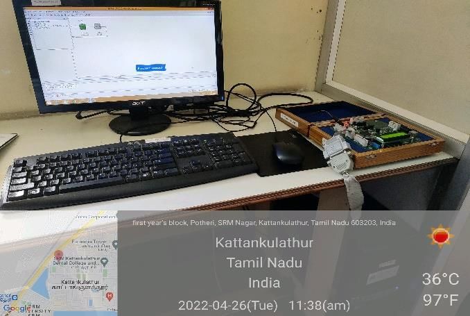
IJIREEICE ISSN (O) 2321-2004, ISSN (P) 2321-5526
International Journal of Innovative Research in Electrical, Electronics, Instrumentation and Control Engineering
Impact Factor 7.047Vol. 10, Issue 4, April 2022
DOI: 10.17148/IJIREEICE.2022.10464
route are automatically included.conducted in order to create an FPGA programming file System Generator automates,
debugs, and implements the design process. Xilinx-based FPGAs are verified. It has a quick response time.HDL co-
simulation interfaces with up to 1000x speedup Increased simulation performance Additionally, the System
Generator enables the use of a black box block to import RTL Simulink and co simulation
2. Interfacing with System Generator Design
A "double" is used in the Simulink environment to represent a number in a simulation. A double is a 64-bit floating-point
number with 2's complement. This number system is inefficient for FPGAs since it requires a lot of resources. When Xilinx
blocks communicate with Simulink blocks, a conversion is required since Xilinx block sets employ n-bit fixed point
numbers . This converter employs Gateway In, Gateway Out, and Sampling.
3. Methodology of implementation of image processing in hardware
As shown in Fig-1, all needed hardware algorithms are implemented between picture pre-processing and image post-
processing. The image source, image viewer, Image Pre Processing, and Image Post-Processing units are all
implemented in Simulink and are common to all image processing applications
Fig -1 Design flow of hardware implementation of image processing
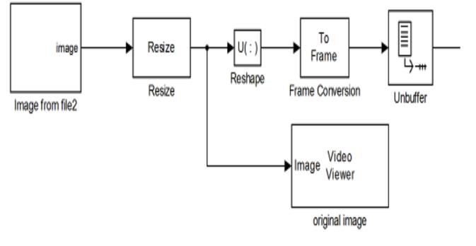
4. Image Pre-Processing Unit
MATLAB image pre-processing aids in supplying FPGA input as a specified test vector array suited for FPGA bit stream
compilation using System Generator.
Fig -2: Image Pre-Processing Unit
Figure 2 depicts the Image Pre-Processing unit block. This unit supports resizing, 2-D to 1-D conversion, frame conversion,
and unbuffering. Because FPGAs only work with one-dimensional data, the conversion from two-dimensional to one-
dimensional data is required.
5. Image Post-Processing Unit
Image post-processing aids in the reconstruction of an image from a one-dimensional array. Data Type Conversion, Buffer,
Convert 1-D to 2-D, and Video Viewer are the four blocks. The first block encodes the image signal as an unsigned integer.
In the second block, scalar samples are converted to frame output at a reduced sampling rate. The third block converts a
one-dimensional picture signal to a two-dimensional image matrix. The output image is displayed on the monitor in the
final block. The Image Post-processing processes are depicted in block diagram form in Figure 3
© IJIREEICE This work is licensed under a Creative Commons Attribution 4.0 International License 419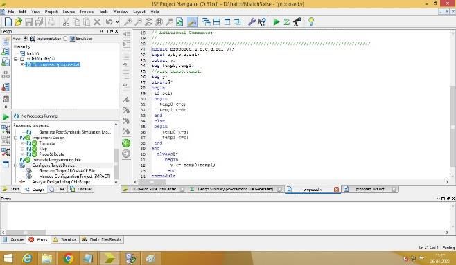
IJIREEICE ISSN (O) 2321-2004, ISSN (P) 2321-5526
International Journal of Innovative Research in Electrical, Electronics, Instrumentation and Control Engineering
Impact Factor 7.047Vol. 10, Issue 4, April 2022
DOI: 10.17148/IJIREEICE.2022.10464
Fig -3: Image Post-Processing Unit
6. Image processing technique using XSG
Between Gateway In and Gateway Out, all Xilinx blocks should be connected. Any technique can be created using those
two blocks. The actual world signal (picture, speech signal, etc.) is floating point, so the gateway in and gateway out blocks
operate as translators to translate the real world signal into the appropriate form.
IMAGE PROCESSING TECHNIQUES USING XILINX BLOCKS
The basic image processing techniques, such as image enhancement, colour to grayscale conversion, image negative, and
picture edge detection, are implemented in this part using Xilinx blocks and then on the VIRTEX5 FPGA
A. Image Enhancement
Image enhancement is the practise of enhancing the interpretability or perception of information in images for human
viewers while also giving better input for other automated image processing processes. The image can be improved by
setting the R, G, and B components to a constant value (90). If the input image is grayscale, there will only be one
component instead of three, namely R, G, and B. We demonstrate how an image can be improved by adding a constant to
each pixel value. Different filtering architectures and Xilinx blocks can be built and created using model-based design for
image filtering. Figures 6 and 7 exhibit the image enhancement algorithms for grey and colour images, respectively.
© IJIREEICE This work is licensed under a Creative Commons Attribution 4.0 International License 420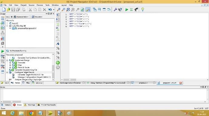
IJIREEICE ISSN (O) 2321-2004, ISSN (P) 2321-5526
International Journal of Innovative Research in Electrical, Electronics, Instrumentation and Control Engineering
Impact Factor 7.047Vol. 10, Issue 4, April 2022
DOI: 10.17148/IJIREEICE.2022.10464
HARDWARE IMPLEMENTATION
The designs described above are only concerned with software simulation. The complete module should be transformed to
an FPGA synthesizable one in order to implement this design in an FPGA board. With the help of the System generating
token, the primary module for any image processing is modified for JTAG hardware co-simulation. A new window will
popup when you click the system generator token, as seen in Fig.15. A bit stream (*.bit) file is generated after this block is
configured for the target platform. After generating the bit stream file, the hardware co-simulation target is chosen, and the
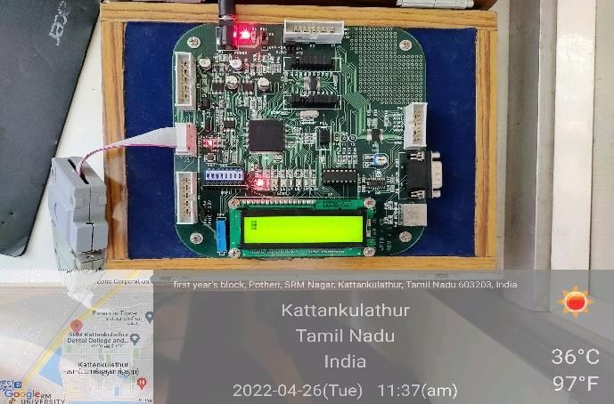
Spartan 3E starting kit (XC3S500E-FG320) is used for board level implementation in this project. A hardware co-
simulation is started after clicking the create button in the System generator block.
Figure depicts the whole architecture for edge detection, including the hardware and software co-simulation design.
The approach can be used in communication systems since it can be applied to arithmetic operations . Each HDL procedure
is designed with its own circuitry if resource sharing is not used. Every addition operation with non-computable operands,
for example, will result in the creation of a new adder.
This hardware repetition expands the design area. However, resource sharing allows many addition operations to be
accomplished with a single adder using time division multiplexing, resulting in hardware savings. As a result, hardware
© IJIREEICE This work is licensed under a Creative Commons Attribution 4.0 International License 421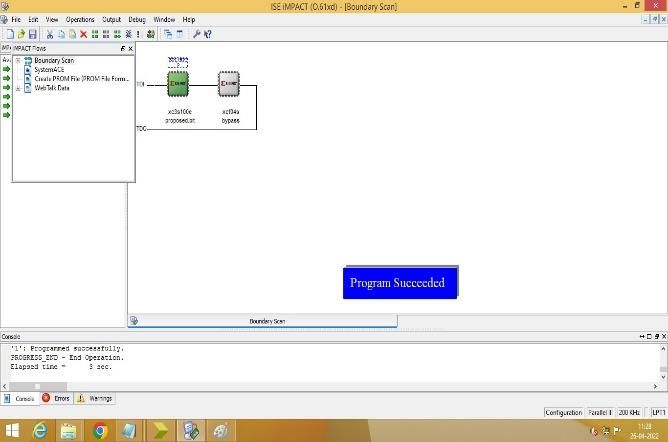
IJIREEICE ISSN (O) 2321-2004, ISSN (P) 2321-5526
International Journal of Innovative Research in Electrical, Electronics, Instrumentation and Control Engineering
Impact Factor 7.047Vol. 10, Issue 4, April 2022
DOI: 10.17148/IJIREEICE.2022.10464
sharing between distinct functionalities can reduce FPGA area . With adjusted inputs, an adder can do subtraction. This
method is referred to as functionality sharing. However, activities can only be shared within the same block or process,
limiting the scope of resource sharing to that process or block. The upper code in Fig employs two adders and a multiplexor,
whereas the lower code makes use of one adder for two separate addition operations.
EXISTING SYSTEM
PROPOSED SYSTEM
DESIGN FLOW FOR IMAGE PROCESSING WITH XILINX SYSTEM GENERATOR
The Simulink model-based design process is used by System Generator. The standard Simulink block sets are frequently
used to produce executable specifications. This specification can be created with floating-point numerical precision and no
hardware detail. System Generator can be used to declare the hardware implementation specifics for the Xilinx devices
once the functionality and basic dataflow concerns have been defined. System Generator will automatically invoke Xilinx
Core GeneratorTM to construct highly efficient netlists for the DSP building blocks when using the Xilinx DSP blockset
for Simulink. System Generator can run all of the downstream implementation tools to create a bit stream that can be used
to programme the FPGA. Test vectors derived from the Simulink environment can be used with ModelSim or the Xilinx
ISE®Simulator to construct an optional test bench.
© IJIREEICE This work is licensed under a Creative Commons Attribution 4.0 International License 422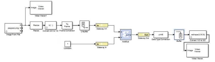
IJIREEICE ISSN (O) 2321-2004, ISSN (P) 2321-5526
International Journal of Innovative Research in Electrical, Electronics, Instrumentation and Control Engineering
Impact Factor 7.047Vol. 10, Issue 4, April 2022
DOI: 10.17148/IJIREEICE.2022.10464
Two software programmes are required to do Image processing tasks using Xilinx System Generator. One is MATLAB
R2011a or higher, while the other is Xilinx ISE 14.1. The MATLAB system generator token that comes with Xilinx must
be setup. This resulted in the inclusion of the Xilinx Block set to the Mat lab Simulink environment, which can be used to
develop algorithmic models directly. Using the Xilinx Blockset library, algorithms and models for picture negative,
improvement, and other purposes are constructed. Xilinx models receive image pixels in the form of a multidimensional
image signal or R|G|B distinct colour signals in the form of a vector in Xilinx fixed-point format. These models are tested
and simulated in the Matlab Simulink environment with appropriate simulation time and simulation mode. A video viewer
can display the reflected findings. System Generator is configured for the appropriate FPGA board after the expected results
are received. The Virtex5 FPGA board was utilised in this project. I/O and clock planning are completed, and the model
for JTAG hardware co-simulation is implemented. The parameters for the System generator are configured and generated.
The netlist is generated during compilation, as well as a model and programming file in Verilog that can be accessed via
Xilinx ISE. The module is tested for behavioural syntax, synthesised, and FPGA implemented. For testing architecture, the
Xilinx System Generator generates User constraints files (UCF), Test benches, and Test vectors. The Xilinx System
Generator (XSG) was built with the intention of dealing with difficult Digital signal processing (DSP) applications, but it
also works with other applications in this field, such as image processing. Bit stream compilation is completed, which is
required in order to generate an FPGA bit file suitable for FPGA input. Figure 2 depicts the Xilinx System Generator design
flow.
© IJIREEICE This work is licensed under a Creative Commons Attribution 4.0 International License 423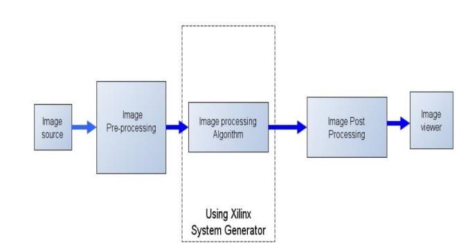
IJIREEICE ISSN (O) 2321-2004, ISSN (P) 2321-5526
International Journal of Innovative Research in Electrical, Electronics, Instrumentation and Control Engineering
Impact Factor 7.047Vol. 10, Issue 4, April 2022
DOI: 10.17148/IJIREEICE.2022.10464
Code implementation Pin configuration
Program uploading to FPGA kit
CONCLUSION
This research concludes that the Xilinx System Generator is a good platform for performing Image Processing in both
software and hardware. It is a versatile tool for image processing, and it provides a quick way to execute complicated image
processing techniques in hardware with minimal resources and latency. It makes Hardware implementation simple and
straightforward. Real-time image processing techniques are developed on FPGA in this paper. The use of huge memory
and inbuilt multipliers allows these algorithms to be implemented on an FPGA. This paper used FPGA to build high-speed
picture enhancing applications. In medical imaging, image enhancing techniques such as brightness and contrast alteration
are critical. Image Enhancement, Image Negative, Image Edge Detection, Image Brightness Control, Image Contrast
Stretching, Range Highlighting Transformation, and Parabola Transformation are all covered in this work.
© IJIREEICE This work is licensed under a Creative Commons Attribution 4.0 International License 424
IJIREEICE ISSN (O) 2321-2004, ISSN (P) 2321-5526
International Journal of Innovative Research in Electrical, Electronics, Instrumentation and Control Engineering
Impact Factor 7.047Vol. 10, Issue 4, April 2022
DOI: 10.17148/IJIREEICE.2022.10464
REFERENCES
[1]. M.Ownby and W.H.Mahmoud, "A design methodology for implementing DSP with Xilinx System Generator for
Matlab," IEEE InternationalcSymposium on System Theory, pp.404-408, March 2003.
[2]. Chandrasekaran, S., Nageswaran, U.B. A mutated addition–subtraction unit to reduce the complexity of FFT. Appl
Nanosci (2022). https://doi.org/ 10.1007 /s13204-021-02278-5.
[3]. Xilinx Inc., " System Generator for Digital Signal Processing" http://www.xilinx.com / tools / dsp.htm.
[4]. Kalyani A. Dakre and Prof. P. N. Pusdekar" "Image Enhancement using Hardware co- simulation for Biomedical",
International Journal on Recent and Innovation Trends in Computing and Communication Volume: 3 Issue: 2.
[5]. R.Srinivasa Rao and R. Nakkeeran , "High level abstraction method for implementing Image Processing Techniques
on FPGA", International Conference on Knowledge Collaboration in Engineering March 27- 28, 2015
[6]. Alareqi Mohammed, Elgouri Rachid and Hlou Laamari, " High Level FPGA Modeling for Image Processing
Algorithms Using Xilinx System Generator ". International Journal of Computer Science and Telecommunications
[Volume 5, Issue 6, June 2014] .
[7]. T. Saidani, D. Dia, W. Elhamzi, M. Atri and R.Tourki, “Hardware Co-simulation for Video Processing Using Xilinx
System Generator,” Proceedings of the World Congress on Engineering, vol.1, Jun 2009. London, U.K
[8]. A. T. Moreo, P. N. Lorente, F. S. Valles, J. S. Muro and C. F. Andres, Experiences on developing computer vision
hardware algorithms using Xilinx system generator” Microprocessors and Microsystems, Vol. 29, pp.411-419 November
2005.
[9]. C.John Moses, D. Selvathi, S.Sajitha Rani, “FPGA Implementation of an Efficient Partial Volume Interpolation for
Medical Image Registration” IEEE International Conference on Communication Control and Computing
Technologies(ICCCCT-10), pp.132– 137,Oct.2010.
[10].Dipikas.Warkar,.Kshirsagar,"FPGA iimplementation of Point Processing Operation using Hardware Simulation",
International Journal of Advanced Research in Computer and Communication Engineering Vol. 4, Issue 4, April 2015.
[11]. R. Gonzalez, R. Woods, “Digital Image Processing” Third edition: Prentice-Hall 2008.
[12]. Ravi.s, Abdul Rahim.B, Fahimuddin shaik," FPGA Based Design and Implementation of Image Edge Detection
Using Xilinx System Generator", International Journal of Engineering Trends and Technology (IJETT – Volume 4 Issue
10 - Oct 2013.
[13]. Abirami AP, DUrga M, Asritha K, Saravanakumar C, " A Time varying capacitance as Load to study area efficient
arithmetic circuits", IEEE International Conference on Advances in Electrical, Computing, Communications and
Sustainable Technologies (ICAECT 2022 ), April 2022
© IJIREEICE This work is licensed under a Creative Commons Attribution 4.0 International License 425
You can also read