BEYOND-NANO: a research infrastructure focused on high performance microelectronics
←
→
Page content transcription
If your browser does not render page correctly, please read the page content below
BEYOND–NANO: a research infrastructure
focused on high performance microelectronics

Corrado Spinella
Director of the Department of Physical Sciences and Technologies of Matter (DSFTM)
corrado.spinella@cnr.it

                                           Accademia Nazionale dei Lincei, Fondazione Edison, 2019, October 30th
Lab_Mat                         Lab_Power                                     Lab_PV

Investigation of materials for   Nanotechnological processes for         Innovative processes for advanced
microelectronics applications    power electronics                       photovoltaics

                                                                         40 Millions of Euros
                                                                         Regione Siciliana: 20 M€
                                                                         Miur:              15 M€
                                                                         Cnr:                5 M€

                                                  Accademia Nazionale dei Lincei, Fondazione Edison, 2019, October 30th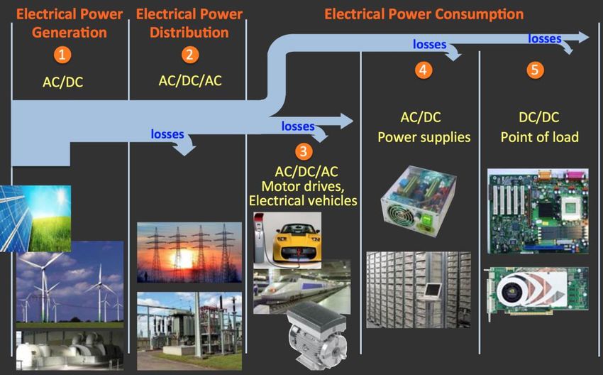
The approach

                From fundamental science to device prototyping

Fundamental science on   Nanofabrication processes            Materials and process
materials properties                                          integration in complex devices

                                       Accademia Nazionale dei Lincei, Fondazione Edison, 2019, October 30th
The Moore Law                                                                                     Improving resolution of microscoy techniques
1000000                                                                                           0.1
                                              price per million
                                              transistors
                                                                                                                                            Aberration–
           10000                                                                                                                           corrected EM

                       100                                                                          1
price $

                                 price per million
                                 instructions per
                         1       second                            35% per
                                                                   year
                                                                   reduction                      10                    Electron
                       0.01
                                                                                                                    Microscope (EM)

                                                                                 resolution (Å)
        0.0001
                 10000                                                                            100
                    1960         1970    1980        1990   2000   2010   2020
                                                     Year
                       1000
 channel length (nm)

                                                                                           1000
                                             gate
                                    source          drain
                        100

                                         channel                                                  104
                         10                                                                                             Light Microscope

                          1                                                                       105
                          1960   1970    1980        1990   2000   2010   2020                     1800      1840       1880      1920       1960      2000       2040
                                                     Year                                                                           Year
                                                                                                    Accademia Nazionale dei Lincei, Fondazione Edison, 2019, October 30th
Atomic resolution Scanning Transmission Electron Microscopy

                                     Beam           STEM
                                     Energy       resolution
                                      (KeV)          (Å)

                                      200            0.68

                                      100            0.83

                                       60             1.1

                                       40            1.36

                                                                                              Ti
                                                                                              Sr
                                                                   (110) Si

       Conventional TEM                       Accademia Nazionale dei Lincei, Fondazione Edison, 2019, October 30th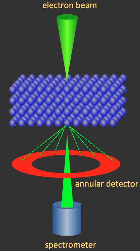
Sub–Ångstrom spatial resolution

                                                             100
                                                                                                                    1 Cq3
                                                                                                                    2 s
                                                                 10

                                                         d (Å)
                       q

                                with a
                                spherical                         1
                                spherical
                                aberration                         0,001              0,01                 0,1                  1
                                    1
                                                                                                                 0.61 l
                                d ≈ Cs q 3
                                aberration
                                    2
                                corrector
Rayleigh limit                                                                                                       q
            l                                                    0.1
 d ≈ 0.61                                                                            0.01                 0.1                   1
            q
                                                                                             q (rad)
Inherent nature of bending of      Inherent nature of the lens
light/electron waves when          used in the imaging system
passes through an aperture
lens of finite size
                                                                              l = 0.025 Å @ 200 kV

                                                            Accademia Nazionale dei Lincei, Fondazione Edison, 2019, October 30th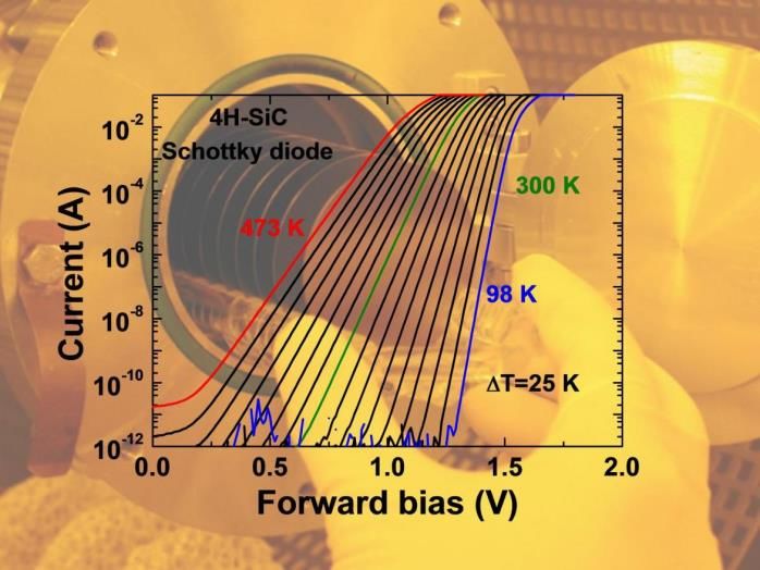
HEXAGONAL                            HEXAGONAL
              ROCK–SALT
                                                               LOW–ORDER                            HIGH–ORDER
              T = 150 °C on SiO2                              T = 350 °C on SiO2                   Epitaxial–Hexagonal
                                                                                        gaps

                                                                                       9
                                                                                             11
                                       Van der Waals forces

                                                                                       9
                                                                                             11
                                                                                       11
                                                                                             11
                                                                                        9
                                                                                             11
                                                                                       11
                                                                                               9

A.M. Mio et al., Nanotechnology 28(6), 065706 (2017)
                                                       Accademia Nazionale dei Lincei, Fondazione Edison, 2019, October 30th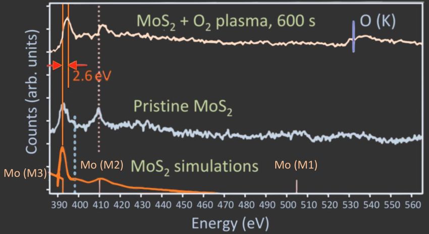
More Moore: memory devices based on novel materials
reset
Phase Change Memories based on chalcogenides
applied pulse
set
0.0 1.0
read read
0.2 0.8
0.4 0.6 regime of fast
temperature
Tm
crystallization
0.6 0.4
0.8 0.2
amorphization
1.0 0.0
conductivity
0.0 0.2 0.4 0.6 0.8 1.0 “1”
Ge at % crystallization “0”
threshold switching
top electrode
time
crystalline GST
Write/Erase velocity
thermal insulator
α/crystalline Scalability
GST
resistor (heater)
High RESET/SET Contrast
Ciclability/Endurance
bottom electrode
20 nm Data Retention
Accademia Nazionale dei Lincei, Fondazione Edison, 2019, October 30th
Nanoscale tailoring of Schottky metal/MoS2 barrier by oxygen plasma
               functionalization
                                                             MoS2 promising material for next generation post–Si
                                                             CMOS technology

                                                             The high effective mass and large bandgap of MoS2 minimize
                                                             direct source–drain tunneling, while its atomically thin body
                                                             maximizes the gate modulation efficiency in ultrashort–
                                                             channel transistors.

                0.4                                                                        0.4
                                                                                                  O2 plasma for
                       pristine MoS2
                0.2                                                                        0.2    10 minutes

                                                                           current (μA)
current (μA)

                0.0                                                                        0.0

               –0.2                                                                       –0.2

               –0.4                                                                       –0.4

                  –4           –2           0            2            4                      –4         –2           0       2         4
                                         Vtip (V)                                                                 Vtip (V)

                 F. Giannazzo et al., ACS Applied Materials 9, 23164 (2017)
                                                                        Accademia Nazionale dei Lincei, Fondazione Edison, 2019, October 30th
After O2 plasma exposure

                                               magnetic prism

             Accademia Nazionale dei Lincei, Fondazione Edison, 2019, October 30th
Ambipolar MoS2 Transistor a
O2 plasma O2 plasma
functionalization functionalization
1.0 10–5
VG = 0 to 28 V 10–6
I/W (A/mm)
L = 10 mm 10–7
0.5 10–8 VDS (V)
10–9 1
I/W (A/mm)
10–10 2
0 5
10–11
1.0
VG = –60 to 0 V
me = 11.5 cm2 V–1 s–1
1.0
I/W (A/mm)
0.5 mh = 7.2 cm2 V–1 s–1
0.5
0 0
0 1 2 3 4 5 –60 –40 –20 0 20
VG (V)
VDS (V)
Accademia Nazionale dei Lincei, Fondazione Edison, 2019, October 30thGlobal energy consumption
900
800
history predictions
700
quadrillion Btu
600
500
400
300
200
100
0
1980 1990 2000 2010 2020 2030 2040
Source: IEA, World Energy Outlook report for 2016
Reducing the CO2 emissions
Electric power distribution chain
CO2 emissions (Gt)
2020 2035
40 current trend
Efficiency 71% 48%
35 Renewables 18% 21%
Biofuels 1% 3%
Nuclear 7% 8%
30
CCS * 2% 19%
25
20 *Carbon capture
2008 2020 2035 and storage
Source: IEA, World Energy Outlook report for 2010
Accademia Nazionale dei Lincei, Fondazione Edison, 2019, October 30thWide band–gap semiconductors Vbd2
Ron ≈
e mn Ecr3
103
specific on–resistance (Ω cm2)
Si 4H–SiC GaN
102
Egap (eV) 1.1 3.2 3.4 101
Ecr (MV/cm) 0.3 3.0 3.3 s 100 Si
10–1
mn (cm2/Vs) 1350 800 1300*
10–2 4H–SiC
k (W/m°C) 150 490 130 10–3
*2DEG 10–4 GaN
Power MOSFET
10–5
10–6 2
RS 10 103 104
breakdown voltage (V)
n+ +
p+ Ra Rch n p+
RJFET Lower Ron reduced device size
Rn n– • Reduction of the static and dynamic losses
• High power conversion efficiency
n+
RD
Accademia Nazionale dei Lincei, Fondazione Edison, 2019, October 30thGrowht of
3C–SiC on 3C–SiC
Si
Si 3C–SiC
Si
6H cluster
0.1 mm
10 Å 10 Å
10 Å 10 Å 10 Å 10 Å
La Via et al., Mat. Sci. Semicon. Processing 78, 57 (2018) Accademia Nazionale dei Lincei, Fondazione Edison, 2019, October 30th4H–SiC Power MOSFET
Issues:
High density of traps at SiO2/SiC interface, low channel
mobility
1150 °C in N2O
SiO2
n+ n+
p+ p+
n– 4H–SiC
n+
Accademia Nazionale dei Lincei, Fondazione Edison, 2019, October 30thSTEM–EELS reveals the presence of a
non–abrupt SiO2/4H–SiC interface
A mixed sp2/sp3 carbon hybridization
in the non–abrupt interface suggests
that the interfacial carbon atoms have
lost their tetrahedral SiC coordination
120
dark field
110
silicon
2400 100
2200
oxygen
90
2000
SiOx nitrogen
counts (arb. units)
s*
counts (arb. units)
80
1800
70 carbon
1600
60
1400
50
SiO2
1200
1000 p* 40
800 30
600 20
285 290 295 300
10
Energy (eV)
0
–20 –10 0 10 20
distance (Å)
P. Fiorenza et al., Nanotech. 29, Art. No. 395702 (2018) Accademia Nazionale dei Lincei, Fondazione Edison, 2019, October 30thTechnology transfer: the silicon carbide example
Energy efficiency – power electronics – silicon carbide
Data center
conversion smart grid IT intelligent building
loss loss
wind loss railway EV/HEV motor drive
transmission
conversion conversion
Thermal distribution conversion conversion conversion
Nuclear generation
Hydro switching
N Innovative Power storage
large scale
power supply
Electronics based on business machine
server
5Å SiC Photovoltaics silicon carbide UPS
Accademia Nazionale dei Lincei, Fondazione Edison, 2019, October 30tha selection of Patents
Manufacture of wafers of wide energy gap semiconductor material for
the integration of electronic and/or optical and/or optoelectronic
devices, US 20140264385 A1, 2014, September the 18th
Semiconductor substrate suitable for the realization of electronic and/or
optoelectronic devices and relative manufacturing process, US 20150031193 A1,
2015, January the 29th
Solar panel having monolithic multicell photovoltaic modules of
different types, US 9006558 B2, 2015, April the 14th
Integrated electronic device for detecting ultraviolet radiation, US
20160349108 A1, 2016, December the 1st
Thin film solar cell module including series-connected cells formed on a flexible
substrate by using lithography, US 9276149 B2, 2016, March the 1st
Thin refractory metal layer used as contact barrier to improve the performance of
thin-film solar cells, US 20160079453 A1, 2017, March the 17th
Avalanche photodiode for detecting ultraviolet radiation and
manufacturing method thereof, US 20170098730 A1, April the 6th
Wide bandgap high-density semiconductor switching device and manufacturing
process thereof, US 9711599 B2, 2017, July the 18th
Multiband double junction photodiode and
related manufacturing process, US 20170207360 Accademia Nazionale dei Lincei, Fondazione Edison, 2019, October 30th
A1, 2017, July the 20thGraphene growth on _ [0001]
_
mis–oriented Si–face [1100]
[1120]
graphene
of the SiC wafer
interface
4H–SiC
Epitaxial graphene: solution for
Si terminated 4H–SiC (0001)
_ substrates 8° off–axis integration of high power and high
miscut angle in the [1120] direction frequency functions on a SiC substrate
(c) 30
30
(nm)
Height (nm)
Height (nm)
100
Height
f
[1-100]
0
400 400 500 400 500 400 500 400 500
L (nm)
[11-20]
00 G. Nicotra et al., Phys. Rev. B 91(15), 155411 (2015)
200 nm
200 nm
Accademia Nazionale dei Lincei, Fondazione Edison, 2019, October 30th(0001) q
Atomic resolution HAADF–STEM
@ 60 keV primary electron beam
_
SiC
5th
4th
3rd
2nd
1st
Cross section perpendicular to
[0001] direction
3.35 Å The buffer layer on the planar
2.64 Å (0001) _surface gets detached from
the (112n) surface
Ab initio simulations showing the equilibrium average atomic distances
Accademia Nazionale dei Lincei, Fondazione Edison, 2019, October 30thπ* σ*
Intensity (a.u.)
_
1st step layer (112n)
2nd layer (0001)
buffer layer (0001)
5Å
28 29 30 31 32 33 34 35 36 37
0 0 0 0 Energy
0 Loss0 (eV) 0 0 0 0
_
The buffer layer present on the planar (0001) face gets detached from the substrate on the (112n)
facets of the steps, turning into a quasi–freestanding graphene film
Accademia Nazionale dei Lincei, Fondazione Edison, 2019, October 30thConductive Atomic Force Microscopy
30
1
20
15
Height (nm)
10
Current (mA)
Height (nm)
5
0
1.0
Current (mA)
0.8
0.6
0.4
0
0
100 nm 100 nm 100 200 300
Length (nm)
When synthesized on a silicon carbide (0001) surface, epitaxial
graphene is subjected to a high electron–doping originating right
from the interface carbon buffer layer that is covalently bonded
to the substrate.
Accademia Nazionale dei Lincei, Fondazione Edison, 2019, October 30thDistributed European Research infrastructure of advanced electron microscopy
ESTEEM3 NTNU
Oxford Univ.
Cambridge Univ.
FZ–Jüelich Krakowie Univ.
Antwerp Univ.
Paris Sud Univ.
Max Planck
FELMI–ZFE
JSI–K7
CEMES
Zaragoza Univ.
Cadiz Univ.
Beyond–Nano
Accademia Nazionale dei Lincei, Fondazione Edison, 2019, October 30thYou can also read