Highly efficient blue organic light-emitting diodes using dual emissive layers with host-dopant system
←
→
Page content transcription
If your browser does not render page correctly, please read the page content below
Highly efficient blue organic light-
                                 emitting diodes using dual emissive
                                 layers with host-dopant system

                                 Bo Mi Lee
                                 Hyeong Hwa Yu
                                 You Hyun Kim
                                 Nam Ho Kim
                                 Ju An Yoon
                                 Woo Young Kim
                                 Peter Mascher

Downloaded From: https://www.spiedigitallibrary.org/journals/Journal-of-Photonics-for-Energy on 20 May 2021
Terms of Use: https://www.spiedigitallibrary.org/terms-of-use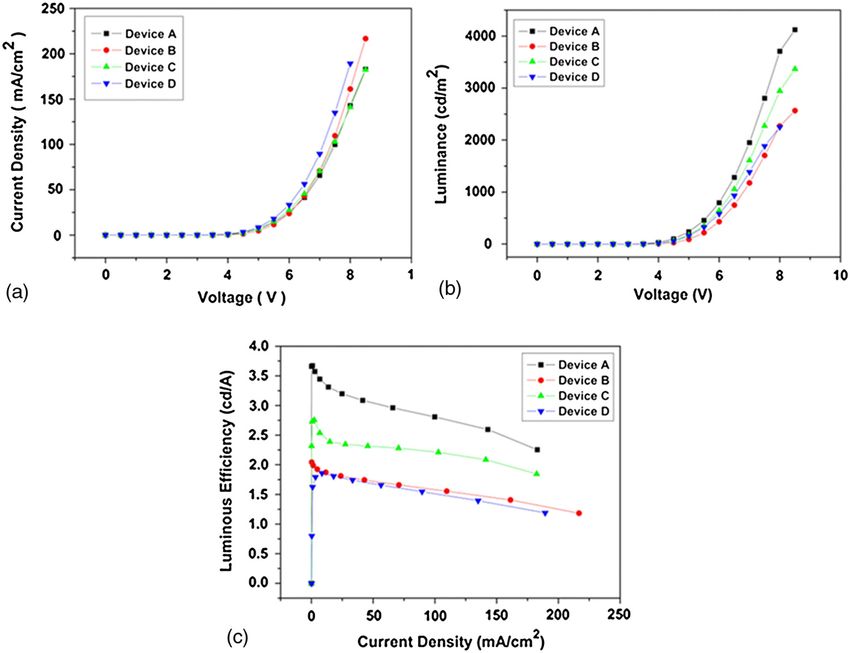
Highly efficient blue organic light-emitting diodes using
                                     dual emissive layers with host-dopant system

                                         Bo Mi Lee,a Hyeong Hwa Yu,a You Hyun Kim,b Nam Ho Kim,b
                                             Ju An Yoon,b Woo Young Kim,a,b and Peter Maschera
                                  a
                                      McMaster University, Department of Engineering Physics and Centre for Emerging Device
                                                        Technologies, Hamilton, Ontario L8S 4L7, Canada
                                                                      mascher@mcmaster.ca
                                         b
                                           Hoseo University, Department of Green Energy and Semiconductor Engineering,
                                                                Asan, 336-795, Republic of Korea

                                 Abstract. We fabricated highly efficient blue organic light-emitting diodes (OLEDs) by design-
                                 ing differing emitting layer structures with fluorescent host and dopant materials of 4,4-bis
                                 (2,2-diphenylyinyl)-1,10-biphenyl and 9,10-bis (2-naphthyl) anthracene as host materials and
                                 4,4’-bis (9-ethyl-3-carbazovinylene)-1,1’biphenyl (BCzVBi) as a dopant material to demon-
                                 strate electrical and optical improvements. Best enhancement in luminance and luminous
                                 efficiency were achieved by a quantum well structure in device F with 8668 cd∕m2 at 8 V
                                 and 5.16 cd∕A at 103.20 mA∕cm2 , respectively. Among the blue OLED devices doped by
                                 BCzVBi, device B emits the deepest blue emission with Commission Internationale de l’É
                                 clairage coordinates of (0.157, 0.117) at 8 V. © The Authors. Published by SPIE under a
                                 Creative Commons Attribution 3.0 Unported License. Distribution or reproduction of this work in
                                 whole or in part requires full attribution of the original publication, including its DOI. [DOI: 10
                                 .1117/1.JPE.3.033598]
                                 Keywords: dual emissive layer; luminous efficiency; blue OLED; quantum well; host–dopant;
                                 4,4-bis (2,2-diphenylyinyl)-1,10-biphenyl; 4,4’-bis (9-ethyl-3-carbazovinylene)-1,1’biphenyl;
                                 9,10-bis (2-naphthyl) anthracene.
                                 Paper 12066P received Dec. 13, 2012; revised manuscript received Feb. 20, 2013; accepted for
                                 publication Mar. 8, 2013; published online Apr. 9, 2013.

                                 1 Introduction
                                 Organic light-emitting diodes (OLEDs) have attracted considerable interests due to their poten-
                                 tial uses, such as full-color displays and solid-state lighting,1–3 when Tang and Van Slyke4
                                 reported the first multilayered OLEDs. Since then, much research has been conducted to improve
                                 OLED performance in terms of efficiency, color stability, and lifetime.5 Specifically to be com-
                                 mercialized, high-quality RGB primary colors are required and blue emission is necessary to
                                 achieve reliable white emission and full-color realization. A lot of effort has been exerted toward
                                 researching blue-emitting materials and improving color purity, as well as the efficiency, of blue
                                 OLEDs, because their performances still lag behind red- and green-emitting materials and devi-
                                 ces.6–8 Major challenges for blue emission correspond to the wide energy band gap of dopants
                                 and matching host materials to achieve blue color, appropriate alignment between blocking
                                 layers and wide gap layers, and high energy exciton confinement.9 In recent years, it has
                                 been accepted that developing deep blue electroluminescence (EL) color with a Commission
                                 Internationale de l’É clairage (CIExy) ‘y’ value of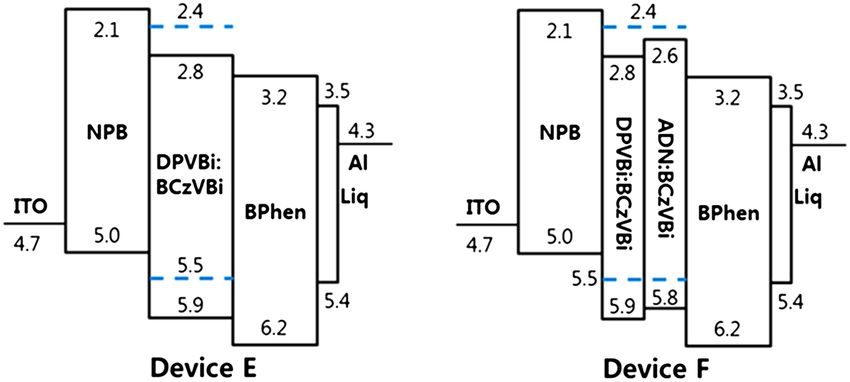
Lee et al.: Highly efficient blue organic light-emitting diodes using dual emissive layers. . .

                                 by the carrier injection and recombination in the emitting layer (EML); therefore, the balance
                                 between electrons and holes in the EML is the most important factor to obtain higher quantum
                                 efficiency.
                                     This study contributes to the understanding of significant effects of double EMLs and
                                 host–dopant systems of blue OLEDs with 4,4’-bis (9-ethyl-3-carbazovinylene)-1,1’biphenyl
                                 (BCzVBi) doped to two different host materials of 4,4-bis (2,2-diphenylyinyl)-1,10-biphenyl
                                 (DPVBi) and 9,10-bis (2-naphthyl) anthracene (ADN). Variable combinations of host and
                                 dopant in single and dual EMLs were observed in blue OLED devices and their electrical and
                                 optical characteristics were compared to each other to achieve best luminous efficiency and blue
                                 color coordinates.

                                 2 Experiment
                                 Indium tin oxide (ITO) coated glass was cleaned in an ultrasonic bath in the order of acetone,
                                 methanol, diluted water, and isopropyl alcohol. Then the cleaned ITO was treated by O2 plasma
                                 under the conditions of 2 × 10⁻² Torr, 125 W for 2 min,21 and organic and metal layers of blue
                                 OLEDs were fabricated using a high vacuum (1.0 × 10⁻⁷ Torr) thermal evaporation.
                                     The standard device structure used in this study is as follows: ITO/N,N’-diphenyl-N,N’-bis
                                 (1-napthyl)-1,1’-biphenyl-4,4’-diamine (NPB) as a hole-transport layer (HTL) (700 Å)/EML
                                 (300 Å)/4,7-diphenyl-1,10-phenanthroline (BPhen) as an electron transport layer (ETL)
                                 (300 Å)/lithium quinolate (Liq) as an electron injection layer (20 Å)/aluminum (1000 Å).
                                 Figure 1(a) shows the molecular structures of the organic materials used in the blue OLED devi-
                                 ces in which the EMLs are composed of DPVBi, and, and BCzVBi, and Fig. 1(b) shows the
                                 schematic diagram of the blue OLED configuration. Six devices with different EML structures
                                 are shown in Table 1 and are classified by different host materials, the sequence of host materials,
                                 and doped or nondoped EMLs. The EML thickness is fixed at 300 Å regardless of the EML
                                 structures.

                                 Fig. 1 (a) Fluorescent host and dopant materials for blue emission, and (b) the standard structure
                                 of blue OLED devices.

                                                        Table 1 EML composition of blue OLED devices A to F.

                                                                                                              EML structure

                                 Device A                                              DPVBi (300 Å)

                                 Device B                                              ADN (300 Å)

                                 Device C                                              DPVBi (150 Å)/ADN (150 Å)

                                 Device D                                              ADN (150 Å)/DPVBi (150 Å)

                                 Device E                                              DPVBi:BCzVBi (15%) (300 Å)

                                 Device F                                              DPVBi:BCzVBi (15%) (150 Å)/ADN:BCzVBi (15%) (150 Å)

                                 Journal of Photonics for Energy                       033598-2                                      Vol. 3, 2013

Downloaded From: https://www.spiedigitallibrary.org/journals/Journal-of-Photonics-for-Energy on 20 May 2021
Terms of Use: https://www.spiedigitallibrary.org/terms-of-use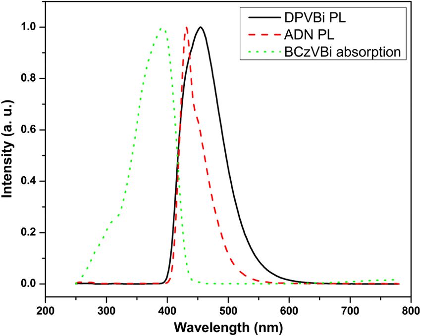
Lee et al.: Highly efficient blue organic light-emitting diodes using dual emissive layers. . .

                                     With various DC voltage biases, the optical and electrical properties of blue OLEDs, such as
                                 the current density, luminance, luminous efficiency, CIExy coordinates, and EL characteristics,
                                 were measured with a Keithley 236, CHROMA METER CS100A and IVL-200 (JBS
                                 International, Korea) OLED analysis system.

                                 3 Results and Discussion
                                 ADN and DPVBi are used as the fluorescent blue emitter in the devices in this paper. As shown
                                 in Fig. 2(a), the current densities of devices A to D are 142.8, 161.2, 141.2, and 189.3 mA∕cm2
                                 at a bias of 8 V, respectively. Typically, the current density is determined by the charge carrier
                                 injection from carrier transport layers22 and the injection is affected by the highest occupied
                                 molecular orbital (HOMO) to the lowest unoccupied molecular orbital (LUMO) energy level
                                 configuration of organic materials in the devices.
                                     In spite of the 0.2 eV higher LUMO energy levels between ADN and BPhen, the higher
                                 current density is achieved in device B with a highly applied voltage because the electron mobil-
                                 ity of ADN is one order of magnitude higher than its hole mobility.23 Devices A and C show
                                 similar curves with variable applied voltage and relatively lower current density, while device D
                                 has the highest current density due to the structural advantage in the energy band diagram, as
                                 shown in Fig. 3. The LUMO of DPVBi is 0.2 eV lower than the LUMO of ADN. These HOMO-
                                 LUMO energy levels in organic layers can explain that device D has a stepped structure with a
                                 lower energy offset between adjacent layers as compared to other devices. This well-arranged
                                 structure leads to more effective electron transport and higher current density than other devices.
                                 In devices A and C, the large energy offset of 0.7 eV between DPVBi and NPB plays a role in
                                 blocking electrons and it consequently leads to the lowest current density.
                                     The plots of luminance versus voltage and luminous efficiency versus current density of
                                 devices A to D are shown in Fig. 2(b) and 2(c). Device A has the highest luminance and
                                 luminous efficiency of 3708 cd∕m2 at 8 V and 2.81 cd∕A at 99.86 mA∕cm2 , and device C
                                 shows second highest luminance of 2946 cd∕m2 at 8 V and 2.21 cd∕A at 102.88 mA∕cm2 ,

                                 Fig. 2 The electrical and optical properties of devices A, B, C, and D; (a) current density–voltage,
                                 (b) luminance–voltage, and (c) luminous efficiency–current density.

                                 Journal of Photonics for Energy                       033598-3                                       Vol. 3, 2013

Downloaded From: https://www.spiedigitallibrary.org/journals/Journal-of-Photonics-for-Energy on 20 May 2021
Terms of Use: https://www.spiedigitallibrary.org/terms-of-use
Lee et al.: Highly efficient blue organic light-emitting diodes using dual emissive layers. . .
Fig. 3 Energy band diagrams of devices A to D.
respectively. Despite device D’s structural advantage; an imbalance of electrons and holes is
caused due to the fact that the ADN with ETL-like material is located next to the HTL. It results
in lower luminance and luminous efficiency. In addition, DPVBi is a bipolar host material so that
better carrier balancing is expected in the DPVBi. Devices A and C, in which DPVBi is placed
next to the HTL, have higher luminance and luminous efficiency than the other two devices,
although they have lower current density.
As can be seen from the device structures of devices A and C in Fig. 3 the large energy offset
with adjacent layers acts as an effective barrier to block carrier flow through the electrodes. Both
NPB and BPhen are used for electron and hole-blocking because of their higher HOMO and
LUMO energy barriers against DPVBi of 0.7 and 0.5 eV, respectively. Therefore, electrons and
holes are confined at the interface between the EML and the blocking layers, causing carrier
balancing, as well as higher recombination probability, in the EML of DPVBi. Moreover, quan-
tum wells are formed in device C to accumulate electrons and holes due to DPVBi’s LUMO and
ADN’s HOMO energy levels. Since most of the recombination zone is generated at the interface
of the EML and the HTL, holes and electrons are likely to be piled up and stocked at the quantum
well, which results in higher luminance and luminous efficiency in device A.
Table 2 summarizes the CIExy coordinates of fabricated blue OLEDs with various voltages.
All measured color coordinates of the devices indicate that they emit deep blue light and the
color coordinates improve with increasing voltage. Device B generates the closest to a deep blue
emission with CIExy coordinates of (0.157, 0.117) at 8 V.
As mentioned above, devices A and C show higher luminance and luminous efficiency com-
pared to the other two devices. Then, we fabricated devices E and F having the same device
Table 2 CIExy color coordinates of devices A to D at voltages of 4, 6, and 8 V.
Device A Device B Device C Device D
4V (0.152, 0.204) (0.161, 0.139) (0.153, 0.160) (0.162, 0.167)
6V (0.152, 0.201) (0.159, 0.126) (0.153, 0.155) (0.158, 0.152)
8V (0.152, 0.198) (0.157, 0.117) (0.153, 0.151) (0.157, 0.141)
Journal of Photonics for Energy 033598-4 Vol. 3, 2013
Downloaded From: https://www.spiedigitallibrary.org/journals/Journal-of-Photonics-for-Energy on 20 May 2021
Terms of Use: https://www.spiedigitallibrary.org/terms-of-useLee et al.: Highly efficient blue organic light-emitting diodes using dual emissive layers. . .
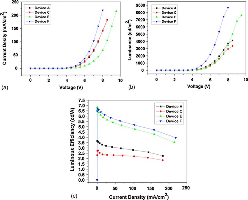
Fig. 4 The electrical and optical properties of devices A, C, E, and F; (a) current density–voltage,
(b) luminance–voltage, and (c) luminous efficiency–current density.
structures as devices A and C, but using BCzVBi dopant in the EML to investigate the effect of
the host–dopant system. The current density versus voltage curve of devices E and F are shown
in Fig. 4. Even though devices A and C have similar current density to each other in the range of
the applied voltage, it is found that device F has significantly higher current density than device E
and the current density of device E is even lower than that of device A. Examining the energy
band diagram of device E in Fig. 5, hole transport readily occurs from NPB to BCzVBi rather
than DPVBi because the HOMO energy level of BCzVBi is 0.4 eV higher than that of DPVBi.
On the other hand, electron transport is blocked by BCzVBi and is more likely to happen to
DPVBi considering the LUMO energy level of DPVBi.
Plots of luminance versus bias voltages and the luminous efficiency versus current densities
of devices E and F are shown in Fig. 4(b) and 4(c). The luminance and luminous efficiency of
device E are 3472 cd∕m2 at 8 V and 4.77 cd∕A at 104.82 mA∕cm2 and that of device F are
8668 cd∕m2 at 8 V and 5.16 cd∕A at 103.20 mA∕cm2 , respectively. Luminous efficiency of
device F is similar to device E at low current density; however, when increasing current density,
Fig. 5 Energy band diagrams of devices E and F using BCzVBi blue dopant.
Journal of Photonics for Energy 033598-5 Vol. 3, 2013
Downloaded From: https://www.spiedigitallibrary.org/journals/Journal-of-Photonics-for-Energy on 20 May 2021
Terms of Use: https://www.spiedigitallibrary.org/terms-of-useLee et al.: Highly efficient blue organic light-emitting diodes using dual emissive layers. . .
Fig. 6 The absorption of BCzVBi dopant and photoluminescence of ADN and DPVBi.
device F shows lower luminous efficiency roll-off compared to device E, because electrons are
trapped at the surface of DPVBi and BPhen in device E due to the LUMO energy gap of 0.8 eV
between BCzVBi and BPhen.
By doping fluorescent BCzVBi into the EML we achieved enhanced luminance in blue
OLEDs compared to nondoped devices due to Förster energy transfer between host and dopant
materials. Förster energy transfer is heavily dependent on the overlap of emission from host and
absorption from dopant. Efficient Förster energy transfer will occur when the exciton energy
from DPVBi host is transferred to BCzVBi dopant, as shown in Fig. 6.
Although device C has dual EMLs, it still has lower luminous efficiency than the single-layer
device A. This is because holes and electrons are confined mainly in the DPVBi layer to lead to
more effective exciton generation in device A. However, the doped dual-EMLs device F shows
higher luminous efficiency than the doped single-layer device E. This result can be explained
with an endothermic energy transfer between the host and dopant material. The endothermic
energy transfer occurs in BCzVBi-doped devices because of the higher LUMO energy level
of BCzVBi than that of DPVBi. The endothermic energy transfer between BCzVBi’s
LUMO and DPVBi’s LUMO is facilitated due to thermal excitation of accumulated electrons
in the LUMO of DPVBi and migration of holes in BCzVBi’s HOMO from DPVBi’s HOMO
energy level. Furthermore, electrons in ADN not only move to the quantum well but also transfer
energy to BCzVBi by endothermic energy transfer and this enhances luminous efficiency of
device F.
The CIExy coordinates of devices E and F are (0.153, 0.252) and (0.153, 0.207) at 8 V, respec-
tively. The color coordinates from devices E and F are far off from those of nondoped devices.
The excitons from BCzVBi-doped EMLs are possibly emitted without enough energy for blue
emission due to the energy level of the host and dopant material; that is, the excitons are trapped
at the HOMO energy level of BCzVBi. In addition, the color coordinates of device F are rel-
atively closer to deep blue emission than that of device E, because ADN has better color purity
when inserted in the EML.
4 Conclusions
Blue OLED devices using single and dual EMLs were fabricated and their electrical and optical
characteristics were compared. A host–dopant system was applied to improve luminous effi-
ciency and color purity based on CIExy coordinates to optimize blue OLED performances.
Among the blue OLEDs, device F with dual EMLs using BCzVBi as a fluorescent dopant
in the host of ADN and DPVBi shows the highest current density, luminance, and luminous
efficiency of 189.3 mA∕cm2 , 8668 cd∕m2 at 8 V, and 5.16 cd∕A at 103.20 mA∕cm2 , respec-
tively, whereas device B emits deep blue emission with CIExy coordinates at (0.157, 0.117) at
8 V. Förster and endothermic energy transfer between host and dopant materials enhanced the
Journal of Photonics for Energy 033598-6 Vol. 3, 2013
Downloaded From: https://www.spiedigitallibrary.org/journals/Journal-of-Photonics-for-Energy on 20 May 2021
Terms of Use: https://www.spiedigitallibrary.org/terms-of-useLee et al.: Highly efficient blue organic light-emitting diodes using dual emissive layers. . .
device’s efficiency. The quantum well structure between the EML, HTL, and ETL plays a role
in improving exciton formation via effective carrier confinement to achieve better device
properties.
Acknowledgments
These works have been financially supported by the Natural Sciences and Engineering Research
Council of Canada under the Discovery Grants program and the Ministry of Knowledge
Economy through the fostering project of the Industrial-Academic Cooperation Centered
University in Korea.
References
1. A. R. Duggal et al., “Organic light-emitting devices for illumination-quality white light,”
Appl. Phys. Lett. 80(19), 3470–3472 (2002), http://dx.doi.org/10.1063/1.1478786.
2. H. Kanno, Y. Hamada, and H. Takahashi, “Development of OLED with high stability and
luminance efficiency by co-doping methods for full color displays,” IEEE J. Sel. Topics
Quantum Electron. 10(1), 30–36 (2004), http://dx.doi.org/10.1109/JSTQE.2004.824076.
3. J. Kido, M. Kimura, and K. Nagai, “Multilayer white light-emitting organic electrolumi-
nescent device,” Science 267(5202), 1332–1334 (1995), http://dx.doi.org/10.1126/science
.267.5202.1332.
4. C. W. Tang and S. A. VanSlkye, “Organic electroluminescent diodes,” Appl. Phys. Lett.
51(12), 913–915 (1987), http://dx.doi.org/10.1063/1.98799.
5. Y. Kijima, N. Asai, and S. Tamura, “A blue organic light emitting diode,” Jpn. J. Appl. Phys.
Part 1 38(9A), 5274–5277 (1999), http://dx.doi.org/10.1143/JJAP.38.5274.
6. Y. Kan et al., “Highly-efficient blue electroluminescence based on two emitter isomers,”
Appl. Phys. Lett. 84(9), 1513–1515 (2004), http://dx.doi.org/10.1063/1.1651653.
7. T. C. Chao et al., “Highly efficient UV organic light-emitting devices based on bi(9,9-diary-
lfluorene)s,” Adv. Mater. 17(8), 992–996 (2005), http://dx.doi.org/10.1002/(ISSN)1521-
4095.
8. S. Tao et al., “Highly efficient non-doped blue organic light-emitting diodes based on fluo-
rene derivatives with high thermal stability,” Adv. Funct. Mater. 15(10), 1716–1721 (2005),
http://dx.doi.org/10.1002/(ISSN)1616-3028.
9. Y. Divayana et al., “Efficient blue organic light-emitting device based on N, N’-di(naphth-2-
yl)-N, N’-diphenyl-benzidine with an exciton-confining structure,” Appl. Phys. Lett. 89(17),
173511 (2006), http://dx.doi.org/10.1063/1.2364161.
10. M. T. Lee et al., “Stable styrylamine-doped blue organic electroluminescent device based on
2-methyl-9,10-di(2-naphthyl) anthracene,” Chen. Appl. Phys. Lett. 85(15), 3301–3303
(2004), http://dx.doi.org/10.1063/1.1804232.
11. M. H. Ho et al., “Highly efficient deep blue organic electroluminescent device based
on 1-methyl-9,10-di(1-naphthyl) anthracene,” Appl. Phys. Lett. 89(25), 252903 (2006),
http://dx.doi.org/10.1063/1.2409367.
12. R. Baer and E. Rabani, “Theory of resonance energy transfer involving nanocrystals: the
role of high multipoles,” J. Chem. Phys. 128(18), 184710 (2008), http://dx.doi.org/10.1063/
1.2913247.
13. J. R. Lakowicz, Principles of Fluorescence Spectroscopy, Springer, New York (2006).
14. Y. Hamada et al., “Red organic light-emitting diodes using an emitting assist dopant,” Appl.
Phys. Lett. 75(12), 1682–1684 (1999), http://dx.doi.org/10.1063/1.124790.
15. C. W. Tang, S. A. Van Slyke, and C. H. Chen, “Electroluminescence of doped organic thin
films,” J. Appl. Phys. 65(9), 3610–3616 (1989), http://dx.doi.org/10.1063/1.343409.
16. A. A. Shoustikov, Y. Yujian, and M. E. Thompson, “Electroluminescence color tuning by
dye doping in organic light-emitting diodes,” IEEE J. Sel. Topics Quantum Electron. 4(1),
3–13 (1998), http://dx.doi.org/10.1109/2944.669454.
17. S. E. Shaheen et al., “Energy and charge transfer in organic light-emitting diodes: a soluble
quinacridone study,” J. Appl. Phys. 85(11), 7939–7945 (1999), http://dx.doi.org/10.1063/1
.370612.
Journal of Photonics for Energy 033598-7 Vol. 3, 2013
Downloaded From: https://www.spiedigitallibrary.org/journals/Journal-of-Photonics-for-Energy on 20 May 2021
Terms of Use: https://www.spiedigitallibrary.org/terms-of-useLee et al.: Highly efficient blue organic light-emitting diodes using dual emissive layers. . .
18. K. M. Vaeth and C. W. Tang, “Light-emitting diodes based on phosphorescent guest/
polymeric host systems,” J. Appl. Phys. 92(7) 3447–3453 (2002), http://dx.doi.org/10
.1063/1.1501748.
19. Y. Kawamura, S. Yanagida, and S. R. Forrest, “Energy transfer in polymer electrophosphor-
escent light emitting devices with single and multiple doped luminescent layers,” J. Appl.
Phys. 92(1), 87–93 (2002), http://dx.doi.org/10.1063/1.1479751.
20. F. C. Chen et al., “Energy transfer and triplet exciton confinement in polymeric electrophos-
phorescent devices,” J. Polymer Sci. Part B. 41(21), 2681–2690 (2003), http://dx.doi.org/10
.1002/(ISSN)1099-0488.
21. C. C. Wu, J. C. Sturm, and A. Khan, “Surface modification of indium tin oxide by plasma
treatment: an effective method to improve the efficiency, brightness, and reliability of
organic light emitting devices,” Appl. Phys. Lett. 70(11), 1348–1350 (1997), http://dx
.doi.org/10.1063/1.118575.
22. S. Y. Oh et al., “Characteristics and fabrication of polymer light emitting diode using
copolymer having perylene and triazine moieties in the polymer side chain,” J. Ind.
Eng. Chem. 12(1), 69–75 (2006).
23. Y. H. Ho et al., “High-efficiency and long-lifetime fluorescent blue organic-emitting
device,” Proc. SPIE 6333, 633303 (2006), http://dx.doi.org/10.1117/12.678220.
Biographies and photographs of the authors not available.
Journal of Photonics for Energy 033598-8 Vol. 3, 2013
Downloaded From: https://www.spiedigitallibrary.org/journals/Journal-of-Photonics-for-Energy on 20 May 2021
Terms of Use: https://www.spiedigitallibrary.org/terms-of-useYou can also read