In-situ Liquid Electrochemical TEM Investigation of Semi Solid-State LMNO Micro-Battery
←
→
Page content transcription
If your browser does not render page correctly, please read the page content below
1044                                                                                                                        Microsc. Microanal. 27 (Suppl 1), 2021
                doi:10.1017/S1431927621003949                                                                                               © Microscopy Society of America 2021

                In-situ Liquid Electrochemical TEM Investigation of Semi Solid-State LMNO Micro-
                Battery
                Ankush Bhatia1, Maxime Hallot2, Sorina Cretu3, Nicolas Folastre4, Maxime Berthe5, David Troadec5,
                Pascal Roussel6, Jean-Pierre Pereira-Ramos7, Rita Baddour-Hadjean7, Christophe Lethien5 and Arnaud
                Demortière4
                1
                  Laboratoire de Réactivité et de Chimie des solides (LRCS), Université de Picardie Jules Verne, CNRS
                UMR 7314, 33 rue Saint Leu, 80039 Amiens Cedex, France, Thiais, France, 2Institut d’Electronique, de
                Microélectronique et de Nanotechnologies, Université de Lille,Centrale Lille,ISEN, Université de
                Valenciennes, CNRS UMR 8520- IEMN, F-59000 Lille, France, Languedoc-Roussillon, France,
                3
                  Laboratoire de Réactivité et de Chimie des solides (LRCS), Université de Picardie Jules Verne, CNRS
                UMR 7314, 33 rue Saint Leu, 80039 Amiens Cedex, France, France, 4Laboratoire de Réactivité et de
                Chimie des solides (LRCS), Université de Picardie Jules Verne, CNRS UMR 7314, 33 rue Saint Leu,
                80039 Amiens Cedex, France, United States, 5Institut d’Electronique, de Microélectronique et de
                Nanotechnologies, Université de Lille,Centrale Lille,ISEN, Université de Valenciennes, CNRS UMR
                8520- IEMN, F-59000 Lille, France, United States, 6Unité de Catalyse et de Chimie du Solide (UCCS),
                Université de Lille, CNRS, Centrale Lille, ENSCL, Université d’Artois, UMR 8181 – UCCS, F-59000
                Lille, France, United States, 7Institut de Chimie et des Matériaux Paris Est (ICMPE), CNRS UMR 7182
                –Université Paris Est Créteil, 2-8 rue Henri Dunant, 94320 Thiais, France, United States
                All-solid-state Li-ion micro-battery is a promising candidate to power miniaturized sensors for the Internet
                of things (IoT) and other electronic devices. In recent times, the spinel LiMn 1.5Ni0.5O4 (LMNO) has
                demonstrated as a potential positive electrode material for Li-ion thin-film batteries offering a theoretical
                capacity of 147 mAh/g (65 µAh/cm2/µm for a bulk density of 4.47 g/cm3) and operates up to now at the
                highest potential (around 4.7 V vs. Li+/Li) [1]. In this work, we report our first successful in situ TEM
                attempts to observe the morphological, structural, and interfacial changes in the positive electrode layer
                of FIB prepared sample which undergo after cycling using liquid electrolyte [2-3]. More precisely we
                compared the morphological and structural evolution between a pristine and cycled micro battery by 4D
                STEM-ASTAR technique to highlight the key information to improve the deposition conditions that will
                enhance the reliability and production quality of such micropower devices.
                Here, our approach is based on cycling a FIB lamella sample inside the TEM using a liquid-
                electrochemical TEM holder with conventional liquid electrolyte (1M LiClO4, EC: DMC 1:1). The cross-
                section image of as-prepared FIB sample with homogeneous deposition of distinctive layers of different
                thickness [from bottom to top-Si (0.385mm)/ Al2O3 (100nm)/ Pt (630nm) / LNMO (400nm)] is shown in
                figure 1a. The Pt current collector of the FIB lamella sample is connected to the Pt working electrode on
                the e-chips used for the TEM study (figure 1b). First, using the FIB preparation technique, we sliced a full
                2-D “thin-film micro-battery” making it as thin to observe/analyze under TEM. Then, we modified the
                FIB lamellar design using the FIB-SEM tool to get good electrical contact and reduced polarisation.
                Several technological problems have to be overcome in the process. For the instance, it is mandatory to
                obtain good electrical contact between the Pt working electrode of the e-chip and Pt current collector of
                FIB lamellar, which is later achieved by depositing extra Pt between the two contacts forming a platinum
                bridge. A 4-Probe electrical conductivity performed locally confirms the good electrical contact between

Downloaded from https://www.cambridge.org/core. IP address: 46.4.80.155, on 24 Oct 2021 at 13:06:38, subject to the Cambridge Core terms of use, available at
https://www.cambridge.org/core/terms. https://doi.org/10.1017/S1431927621003949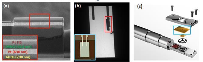
Microsc. Microanal. 27 (Suppl 1), 2021 1045
the as prepared FIB lamella sample and Pt working electrode of e-chip. The cross-section bright-field
TEM image of a final modified version of the FIB lamella sample used in the study is shown in figure 2a.
The FIB lamella sample is then later cycled inside the liquid electrochemical TEM holder (fig 1c) in a
potential window of 4.1 V-4.8 V vs. Li+/Li. The flow of the electrolyte (LiClO4 EC: DMC 1:1) inside the
TEM holder was further controlled by the microfluidic controller with a flow rate of 2 µL/min. CV was
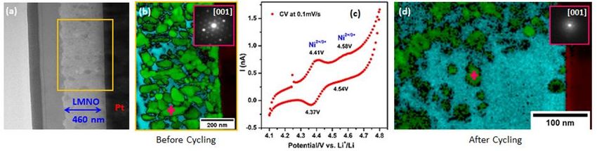
recorded at a sweep rate of 0.1mV/s and two plateaus at 4.4 V and 4.6 V were observed corresponding to
Ni2+/3+ and Ni3+/4+ oxidation respectively (Fig 2c). The basic redox steps observed during the charge are
same as observed in the case of cycling bulk 2D thin film in a homemade flat cell.
The comparison between the cycled and pristine micro battery sliced by FIB and observed by TEM
allowed us to clearly demonstrate the formation of cracks inside the LMNO layer, loss of contact between
the LMNO layer and the platinum current collector, as well as the agglomeration of the organic
compounds produced due to the electrolyte decomposition. Moreover, the 4D STEM-ASTAR technique
[4] provided us with crucial information regarding the grain size reduction from 20 nm in pristine to 12
nm in the cycled sample, confirming the continuous electrode-electrolyte reaction happening over the
cycling. Also, the decrease in crystallinity and increase in the amorphization of the LMNO grains by 38
% in the cycled sample compared to pristine as shown in figure 2b and 2d clearly prove the fast capacity
fading phenomenon observed in the bulk micro battery. Furthermore, a thickness of ~20nm along the
platinum layer, a (111) preferred orientation is observed exhibiting the epitaxial effect of LMNO on the
platinum layer which has been further supported by the precision electron diffraction (PED) recorded on
both LMNO and platinum grains.
Acknowledgments
Ankush Bhatia and Arnaud Demortière acknowledges the French ANR project “CASSIOPES”
N°17-CE09-0016-03 for a Ph.D. grant. We would like to thank Dr. Muriel Veron and Dr. Edgar Rauch
for the fruitful discussions on the ASTAR experiments.
Figure 1. (a) Cross-section image of as-prepared FIB sample with homogeneous deposition of distinctive
layers of different thickness, insert in the red box shows the zoom of the different layers; (b) TEM image
exhibiting the connection between the platinum current collector of FIB sample with the platinum working
electrode of e-chip; insert figure shows the reference and the working electrode on the silicon nitride
window; (c) schematic description of the Poseidon 510 TEM holder ( Protochips) for electrochemical
measurements used in this study.
Downloaded from https://www.cambridge.org/core. IP address: 46.4.80.155, on 24 Oct 2021 at 13:06:38, subject to the Cambridge Core terms of use, available at https://www.cambridge.org/core/terms.
https://doi.org/10.1017/S1431927621003949
1046                                                                                                                        Microsc. Microanal. 27 (Suppl 1), 2021

               Figure 2. (a) Bright-field transmission electron microscopy of the LMNO FIB lamella sample before
               cycling; (b) phase map before cycling where dark red represents the platinum, in green the LMNO phase,
               and in blue the amorphous phase; insert bright red shows the electron diffraction pattern of spinel LMNO
               in [001] orientation; (c) Cyclic voltammogram measured in a holder with a voltage sweep rate of 0.1 mV/s
               in the voltage window of 4.1 V- 4.8 V vs. lithium using 1M lithium perchlorate in EC:DMC electrolyte;
               (d) phase map after cycling where dark red represents the platinum, in green the LMNO phase and in blue
               the amorphous phase; insert bright red shows the electron diffraction pattern of spinel LMNO in [001]
               orientation.

               References
               [1] M. Hallot, A. Demortière, P. Roussel, C. Lethien, Energy Storage Materials, (18)30779-7
               [2] O.M. Karakulina, A. Demortière, W. Dachraoui, A.M. Abakumov, J. Hadermann, Nano lett. 18(2018)
               6286-6291.
               [3] L. Lutz, W. Dachraoui, A. Demortière, L. R. Johnson, P. G. Bruce, A. Grimaud, J.M. Tarascon, Nano
               Lett. 18(2018), 1280-1289
               [4] E. F. Rauch, M. Véron, Mater. Charact. 98 (2014), 1–9.

Downloaded from https://www.cambridge.org/core. IP address: 46.4.80.155, on 24 Oct 2021 at 13:06:38, subject to the Cambridge Core terms of use, available at https://www.cambridge.org/core/terms.
https://doi.org/10.1017/S1431927621003949
You can also read