Mapping China's semiconductor ecosystem in global context - Strategic Dimensions and Conclusions
←
→
Page content transcription
If your browser does not render page correctly, please read the page content below
June 2021 ∙ John Lee & Jan-Peter Kleinhans

Mapping China’s
semiconductor
ecosystem in
global context
Strategic Dimensions
and Conclusions

Policy Brief
June 2021
China’s semiconductor ecosystem

Executive Summary
Historically, the semiconductor value chain has flourished thanks to transnational
divisions of labor that supported high levels of economic efficiency and innovation.
As a result, interdependencies throughout this value chain exist between different
regions around the globe. The US-China technology rivalry, the COVID19 pandemic
and global shortages in semiconductors have led many governments to scrutinize
these interdependencies in the transnational semiconductor value chain. The US
government for example has completed a review of the semiconductor supply chain.
Europe’s new industrial strategy focuses on assessing and managing strategic de-
pendencies in different technology ecosystems, including semiconductors.

China’s capabilities in the semiconductor value chain play a key role in these con-
siderations. China’s government is making great efforts to raise the competitiveness
of Chinese industry in the semiconductor sector, building on and supporting China’s
role in global electronics manufacturing and emerging technological ecosystems.
With growing strategic concerns in the US and Europe about China, a better un-
derstanding and systematic assessment of China’s capabilities in producing semi-
conductors is needed. What is the position within the semiconductor value chain
of Chinese companies? In which areas is China highly reliant on foreign technology
providers? How likely is China to catch up within this decade in a particular produc-
tion step?

This report provides a framework for assessing the national interest vis-à-vis Chi-
na’s role in the semiconductor value chain. We draw conclusions across three stra-
tegic dimensions – industry competitiveness, national security and resilience of the
global supply chain – that impact the interests of all nations, given the importance
of semiconductors in the modern world. Understanding China’s role throughout the
value chain in terms of these strategic dimensions helps policy makers to identify
current and future interdependencies with China, and to balance or prioritize be-
tween competing interests. With this picture, European decisionmakers are better
equipped to best position EU countries for a world in which technological interde-
pendence is increasingly contested, weaponized and fraught with national risk.

2
Policy Brief
June 2021
China’s semiconductor ecosystem

Table of Contents

Executive Summary	                                                        2

Introduction	                                                             5

1. Analytical approach 	                                                  7
    Focus on the value chain                                              7
    Assessment of strategic dimensions for each production step           8

2. China’s semiconductor ecosystem	                                      12
    Larger national policy context                                       12
    China’s policy for the semiconductor industry over the past decade   12
    The future of China’s policy for the semiconductor sector            17
    Situation and prospects for China’s semiconductor sector             18

3. Analysis of the production steps	                                     21
    Chip Design ( process step )                                         21
    Electronic Design Automation ( input )                               25
    Intellectual Property ( input )                                      30
    Wafer Fabrication: The Front-End ( process step )                    34
    Equipment ( SME ) ( input )                                          40
    Chemicals and Materials ( input )                                    45
    Wafers ( input )                                                     48
    Assembly, Test and Packaging: The Back-End ( process step )          51

4. Conclusion and implications for Europe	                               57

Annex 1: Technical Terms Glossary	                                       60

Annex 2: Chinese Terms and Acronyms Glossary	                            62

Annex 3: Chinese official policy documents and
selected other sources 	                                                 64

References	                                                              73

3
Policy Brief
June 2021
China’s semiconductor ecosystem
This joint project between Stiftung Neue Verantwortung ( SNV ) and the Mer-
cator Institute for China Studies ( MERICS ) was made possible by the gener-
ous support of the German Federal Foreign Office. The views expressed in this
paper do not necessarily represent the official positions of the ministry.
The authors would like to thank ( in alphabetical order ) Douglas Fuller, Stew-
art Randall and John VerWey for substantial feedback and helpful discus-
sions about earlier drafts of this report. Furthermore, the authors would like
to thank ( in alphabetical order ) Juliana Bouchaud ( MERICS ), Tashi Götzmann
( MERICS ) and Julia Hess ( SNV ) for their help preparing this report.
4Policy Brief June 2021 China’s semiconductor ecosystem Introduction Semiconductors are the foundation of almost every application of electronics. Often combined in an “integrated circuit” ( IC ) and commonly called “chips,” semiconduc- tors are a strategic technology on which national power is increasingly dependent. Yet their value chain is among the most globalized of any industry. This value chain is extensive, complex and built on a transnational division of la- bor, due to economic pressure to innovate and thus, to specialize. This division of labor has created a host of cross-border interdependencies, with different global regions specializing in different production steps. A particular semiconductor of- ten is designed in the United States ( US ), manufactured in Taiwan using chemicals from Japan and Germany and equipment from the Netherlands, and assembled and packaged in China. Within this complex value chain, many process steps and inputs are indispensable but are often under the control of only a few companies. In some cases, a particular input can be effectively monopolized by a single company. The transnational nature of the value chain conflicts with the national interest per- spective now increasingly brought to the semiconductor sector by governments, politicians and policy commentators. What exactly “strategic importance” means in the context of the semiconductor value chain is often not well articulated. However, these policy debates recognize the critical role of the value chain’s end products in a range of applications, and the potential for the value chain’s interdependencies to be ‘weaponized’ by one nation against another.1 These national interest factors are driving efforts to reduce dependency on foreign providers by strengthening the domestic semiconductor ecosystem—the complex of enterprises, research institu- tions, skilled labor, investment capital and other factors that underpin research and development ( R&D ) and production. Given growing political concerns in Western countries about China, China’s position in the semiconductor value chain and in the applications built on top of chips is seen as a potential threat that must be mitigated. But the cost of mitigation meas- ures based on cutting China out of the global value chain is potentially large, and the success of such efforts uncertain.2 It is also unclear whether European nations would benefit from such decoupling to the same degree as the US and other players in the semiconductor value chain. The starting point for such discussions should be a comprehensive understanding of China’s semiconductor ecosystem, its role in the global value chain and the implications from a national interest perspective, with as much specificity as possible. 5
Policy Brief
June 2021
China’s semiconductor ecosystem

This report provides an overview of China’s position in the semiconductor value chain
by analyzing its position in the different production steps and providing an analyti-
cal framework for drawing conclusions about the strategic implications. In section
1, we explain our general approach focusing on the value chain’s distinct production
steps, and for each step, on China’s domestic ecosystem in the global context. For
each step, we offer conclusions from a national interest perspective, organized by
three strategic dimensions that capture the differing implications of these interests.

In section 2, we provide an overview of China’s semiconductor ecosystem in general,
focusing on the most recent phase of state-led policy for the semiconductor sector.
In section 3, we analyze the eight distinct production steps in the value chain sepa-
rately, following the template described in section 1. Glossaries for technical terms
and for Chinese institutions and documents ( including acronyms ) are provided in
annexes 1 and 2, respectively, at the end of the report. A list of selected Chinese
documents concerning the semiconductor sector is provided in Annex 3.

In section 4, we draw summary conclusions about China’s role in the global value
chain as a whole, focusing on important takeaways for European policymakers. A
second report published in late 2021 will look further into these conclusions in the in-
ternational context and offer policy recommendations from a European perspective.

6
Policy Brief
                       June 2021
                       China’s semiconductor ecosystem

                       1. Analytical approach

                       Focus on the value chain

                       Because the global semiconductor value chain is fragmented functionally and geo-
                       graphically, it should be understood within the context of distinct production steps.
                       We identify eight production steps: They consist of three process steps ( design,
                       fabrication, and assembly, test and packaging ) and five inputs in the process steps
                       ( software, intellectual property ( IP ), equipment, chemicals and wafers; see Fig. 1 ).

             Fig. 1:
Production steps
  ( process steps
and inputs ) in the
  semiconductor
      value chain

                       Focusing on these generic production steps allows us to analyze the competitive-
                       ness of China’s domestic semiconductor value chain, its dependence on foreign
                       technology providers and the likelihood of China’s increased self-reliance and inter-
                       national competitiveness in the future. In section 3, we look at all eight production
                       steps separately, China’s position within them and the implications from a national
                       interest perspective, according to the following template:
                       • Overview: What is the general function of the production step, and how does it
                          relate to the rest of the value chain?
                       • Market structure: What is the current market situation? Who are the dominant
                          players? Are there monopolies or oligopolies?
                       • Barriers to entry: How hard would it be for a new company to enter this market
                          profitably?
                       • The Chinese government’s effort to increase self-reliance: To what extent has
                          the production step received policy attention from the Chinese government? How
                          effective has this been?

                       7
Policy Brief
June 2021
China’s semiconductor ecosystem
• Competitive position of the Chinese industry: What is the competitive position of
Chinese companies in this production step?
• Likelihood of China catching up within 5 to 10 years: How likely is it that China’s
industry will catch up with the global market leaders in the coming decade?
• Strategic dimensions: How do these elements affect national interests, in gener-
al terms and in relation to China’s position in this specific production step?
Assessment of strategic dimensions for each production step
After mapping each production step based on the template above, we offer a short
assessment of the strategic importance of the step. We structure this assessment in
terms of three strategic dimensions. Each dimension corresponds to three criteria
for assessing strategic importance, which distill insights from the mapping. These
dimensions and criteria represent different aspects of national interest. Together,
they explain why in the context of a particular production step governments are mo-
tivated to take measures that promote their own industry and that of allies or con-
strain the capabilities available to adversaries.
Strategic dimensions and criteria
The competitiveness dimension captures commercial and technical implications of
the production step’s market landscape, which affect the economic and technolog-
ical bases of national power, in the context of a competitive international environ-
ment. Criteria include the following:
• Revenue capture: The financial returns that accrue with dominant market share.
Financial returns vary between production steps, with some significantly more
lucrative than others.
• Barriers to entry: The difficulty of a new player establishing itself in this produc-
tion step. High barriers to entry are significant when dominant market share is
held by a few actors, because they make efforts to replicate these capabilities
costly and uncertain of success.
• Spillover benefits: The potential for capabilities in this production step to stimu-
late activity elsewhere in the value chain, or in other industry sectors.
The national security dimension involves a production step’s significance for ze-
ro-sum competition between nation-states. These implications reflect the potential
for ‘weaponization’ by national governments to actively damage the interests of oth-
er nations. Criteria include the following:
• Espionage risk: The potential for manipulation of a given production step to facil-
itate intelligence gathering against or sabotage of the interests of rival nations.
8Policy Brief
June 2021
China’s semiconductor ecosystem
For example, assembly, test and packaging ( ATP ) present relatively significant
opportunities for espionage activity.
• Military utility: The significance to national military capabilities. For example,
chip design capabilities are more important than those in ATP for the capacity of
a national economy ( or an alliance of economies ) to build sophisticated military
platforms, such as fighter aircraft.
• Chokepoint: The potential for dominant market share in a production step to be
weaponized against nations lacking these capabilities, for example, through na-
tional and multilateral export controls that target specific nations.
The resilience dimension addresses the semiconductor value chain as a whole, that
is, on a global scale. As the value chain is globally integrated, disruptions have nega-
tive impacts on national interests generically, regardless of adversarial relations be-
tween particular nations. Every nation suffers from a resilience failure that disrupts
the international value chain as a whole. Criteria include the following:
• Concentrated point of failure: These failure points represent business continuity
risks to the global value chain as a whole from natural disasters, pandemics or
political interventions. Such points are a product of decades of technical spe-
cialization and transnational division of labor.
• Spillover damage: This represents the potential for the disruption of a given pro-
duction step to flow to other segments of the global value chain, and to other
industrial sectors. An example can be seen in the current problems facing the au-
tomobile manufacturing industry worldwide, stemming from constraints in wafer
fabrication.
• Replicability: The implications of attempting to replicate a given production step,
through government intervention, in nations where it is not currently concentrat-
ed. Replicating production in this way can increase the global value chain’s resil-
ience through national and geographic diversification. However, such efforts also
risk wasting resources and hampering innovation, by changing the economies of
scale and transnational division of labor that have given the semiconductor value
chain its current form.
Distinguishing between these strategic dimensions allows us to understand why a
national government would try to strengthen its own semiconductor ecosystem, in-
cluding in cooperation with allies, or to undermine that of its adversaries. For exam-
ple, even if there are few economic reasons ( such as low revenue capture, high bar-
riers to entry ) to invest in domestic capabilities for a particular production step, if it
constitutes a chokepoint for domestic industry due to reliance on foreign technology
providers, a nation might try to strengthen its own industry in that production step.
9Policy Brief June 2021 China’s semiconductor ecosystem These strategic dimensions in each production step are not specific to China: Bar- riers to entry, espionage risk, spillover damage and the other criteria all have the same implications from the perspectives of all nations. Thus, our matrix ( see Fig. 2 ) provides a generic overview or heat map of the semiconductor value chain across the strategic dimensions we describe in the mapping. The color codes show to what extent one of the criteria applies to a specific production step. For example, the bar- riers to entry ( for any company, in any nation ) for a given production step can be low, moderate, substantial or high. The matrix provides the basis for assessments in the strategic dimensions section in each production step chapter. In these sections, we explain the strategic impor- tance of each production step, listed by the criteria we described above. We also provide conclusions specifically about China’s current position in each production step and the country’s likely progress over the next decade. We evaluate China’s be- havior and include evaluations of responses by other nations. For example, the military utility of end products based on chip design capabilities is a substantial reason for the Chinese government to promote chip design capabili- ties domestically, but from a U.S. viewpoint, this is a substantial reason to restrict such development in China. These imperatives are compounded by the progress Chi- na has made in this production step, as well as China’s potential to support further progress with demand for semiconductors generated by other sectors of the Chi- nese economy. This approach helps the reader to compare national interests and risks that differ in type and operate in different contexts, which potentially implies conflicting choices in response. What to prioritize, and how to resolve trade-offs, are for the reader to decide. In the conclusion in section 4, we highlight what we consider the most im- portant issues from a European viewpoint. The following examples illustrate how to read this matrix, in conjunction with the strategic dimensions analysis for each production step: • Design: Given high revenue capture, high spillover benefits and low barriers to entry, China will likely continue to substantially support its domestic chip design ecosystem. China also has substantial incentives in terms of potential benefits for supporting the development of chips that have military utility, representing a source of risk for nations that view China as a potential adversary. • SME: Despite a relatively low revenue capture and substantial barriers to entry, China will try to decrease its reliance on foreign semiconductor manufacturing equipment ( SME ) vendors because SME provides the US and its allies with a substantial chokepoint to exploit against China. If China succeeds in establish- ing competitive domestic SME vendors, there will be substantial spillover bene- fits, because SME is a critical input for wafer fabrication. 10
Policy Brief
                     June 2021
                     China’s semiconductor ecosystem

                     •    ATP: Assembly, test and packaging ( ATP ) has relatively low revenue capture and
                          currently, only moderate spillover benefits. As the importance of advanced pack-
                          aging is increasing, these aspects will certainly change in the future. The high
                          espionage risk associated with this production step is of little concern to China,
                          as it holds a substantial share of the packaging market. Thus, it is highly likely
                          that China will try to upgrade its packaging ecosystem to ensure a strong market
                          position in the future.

Fig. 2: Strategic
dimensions per
production step
      ( overview )

                     11
Policy Brief
June 2021
China’s semiconductor ecosystem
2. China’s semiconductor ecosystem
Larger national policy context
China’s policy for the semiconductor sector sits within a larger framework for sci-
ence and technology development, which is articulated in various directive policy
statements issued by China’s central government authorities. Key principles under-
lying this framework include the following:
• The assessment that information technology ( IT ) and digitalization have become
foundational to national economies and therefore, to national power, in a com-
petitive international environment;
• The continued centrality of the physical ( “real” ) economy and manufacturing,
and the need to deeply integrate the real economy with IT to achieve broad-based
technological leadership;
• Recognition that China is still lagging global leaders in core technologies, a
source of national vulnerability that must be mitigated by increasing China’s rel-
ative capabilities;
• Recognition that closing the gap in technological capabilities requires maintain-
ing a degree of international openness in China’s economy and connections to
foreign technological leaders.
China’s policy for the semiconductor industry over the past decade
Semiconductors have been targeted by official Chinese policies for several decades,
although progress in closing the gap with foreign industry leaders across the value
chain remains limited.3 In the following paragraphs, we describe the important as-
pects of the most recent phase of Chinese official policy for the semiconductor sec-
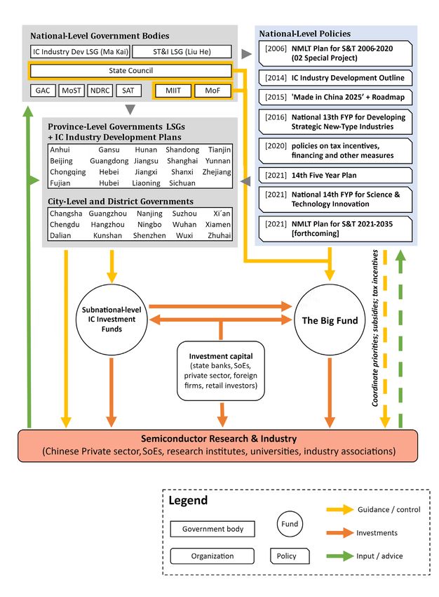
tor. These aspects are captured by a schematic representing how Chinese state-led
policy operates across the entire sector ( Fig. 3 ).
China’s senior leaders seem to have understood Chinese industry’s critical foreign
dependencies since at least 2009, when national agencies instituted the 02 Special
Project. This aimed to “break China’s dependence on imports” across various seg-
ments of the semiconductor value chain, by assigning R&D projects to enterprises
and research institutions.4 A 2017 progress report identified some successes5: For
example, it claimed that Chinese suppliers had commercialized 16 types of front-
end wafer fabrication equipment; one product was approved by global foundry lead-
er TSMC for an advanced ( 7 nanometer, ‘nm’ ) process node.6
12Policy Brief June 2021 China’s semiconductor ecosystem The 2014 National IC Industry Development Outline In 2014, the State Council, China’s highest executive government agency, issued the National Integrated Circuit Industry Development Outline ( the 2014 Outline ). This is often identified as starting the current phase of China’s semiconductor policy, marked by less direct state intervention than in the past and by extensive state-led funding across the board rather than favoring of a few selected firms.7 The 2014 Outline sought to improve centralized policy coordination by creating a national steering committee ( Leading Small Group, LSG ), supported by an adviso- ry expert committee. The IC Industry LSG’s director is a Vice-Premier of the State Council and member of the Chinese Communist Party’s ( CCP ) Politburo, Ma Kai, and its deputy director ( often the key executive role in such bodies ) is the head of the Ministry of Industry and Information Technology ( MIIT ), Miao Wei. Both men hold corresponding positions in a separate LSG for “building China into a manufactur- ing superpower,” reflecting the connections between semiconductors and the wider electronics and manufacturing sectors.8 It is unclear to what extent the national IC LSG remains active or involved in pol- icymaking. In June 2021, media reporting suggested that the impetus behind na- tional-level policymaking for the semiconductor industry was shifting to the LSG for ‘reform of the national science and technology system and building an innova- tion system’ ( ST&I LSG ).9 This body is headed by Liu He, chief economic adviser to Chinese President Xi Jinping, and China’s lead negotiator for trade talks with the U.S. government during the Trump administration. The precise relationship between these two LSGs is unclear. The same is true for the extent of coordination with ‘lead- ing small groups’ for semiconductor policy created by several subnational govern- ments in the last few years ( Annex 2 ). The 2014 Outline listed development targets for chip design, fabrication, packaging and test, manufacturing equipment and materials.10 It aimed to promote upgrades in all these segments of the value chain through direct financing and tax relief meas- ures, and through state-linked equity investment funds at the national and regional levels.11 Accordingly, the 2014 Outline established the National Integrated Circuit In- dustry Investment Fund ( Big Fund ), incorporated in late 2014 with registered capital of RMB 98.72 billion ( more than USD 15 billion ). State-linked investment funds The Big Fund represents a type of state-led industrial policy instrument now com- mon in China across foundational and emerging technology sectors: the so-called 13
Policy Brief
June 2021
China’s semiconductor ecosystem

‘government guidance fund.’ Such funds use the limited partnership structure typ-
ical of equity finance worldwide, but they are set up by state agencies that provide
anchor capital and influence investment decisions. State involvement aims to at-
tract investment from other sources such as China’s private sector and foreign in-
vestors, although in practice a dominant role is often played by state-owned en-
terprises and other state-linked actors.12 These state-linked investment funds may
also be a means of avoiding World Trade Organization ( WTO ) restrictions on direct
subsidies: the Big Fund was named in a U.S. complaint at the WTO in 2018.13

The Big Fund is overseen by the MIIT and the Ministry of Finance.14 Most sharehold-
ers are state-owned enterprises and other government guidance funds; the bulk of
the capital raised during Phase I came from the Ministry of Finance and the state-
owned China Development Bank ( CDB ).15 The Big Fund’s managing entity ( Sino-IC
Capital ) has been run in succession by two executives from CDB, which also owns
45% of Sino-IC.16

Subnational IC investment guidance funds were also established during 2014 in ex-
isting centers of China’s semiconductor industry.17 The Shanghai government-linked
fund was established in partnership with a private investment fund, a common mod-
el for government guidance funds that seeks to leverage private sector expertise.18
As of mid-2020, 14 province-level governments had set up their own investment
funds for the IC sector, totaling around RMB 300 billion ( USD 45 billion ).19

Phase I of the Big Fund closed in 2019, having raised RMB 138.7 billion ( more than
USD 20 billion ).20 Around two thirds of the fund’s investments went to fabrication
and the other manufacturing-related categories of SME and materials, while ap-
proximately 20% were made in the chip design sector and around 10% in assembly,
test and packaging.21 At the close of Phase I, Sino-IC Capital declared that the total
capital expenditure in China’s semiconductor sector had doubled over 2014–2017,
compared to the preceding four years.22 Chinese state media reported that Phase I
attracted five times the sum of capital it raised ( that is, around RMB 500 billion ) to
China’s semiconductor sector from other financing sources.23

Phase II of the Big Fund was incorporated in October 2019 with registered capital
of RMB 204.15 billion ( more than USD 32 billion ). The shareholder mix expanded to
include entities representing a wider geographical spread of China’s semiconductor
sector, which may improve the overall quality of the investments.24 The state hopes
that Phase II achieves the same 1:5 investment multiplier ratio that was claimed for
Phase I.25 This would result in an additional RMB 1 trillion ( more than USD 150 bil-
lion ) of investment in China’s semiconductor sector. However, this amount of funding
does not appear to be guaranteed by Chinese authorities, although it is sometimes
portrayed this way in international media reporting.

14
Policy Brief
June 2021
China’s semiconductor ecosystem

The Big Fund’s Phase I prioritized investments in fabrication, as directed in the 2014
Outline. Chinese state media reporting when Phase II was incorporated indicated
that future investments would focus more on SME and on applications downstream
in the value chain, thus dragging along development of upstream sectors. Cited as
precedent for such an outcome is the previous upgrading of China’s mobile device
supply chain that was driven by Apple’s manufacturing operations in China.26

Other supporting policies for the semiconductor sector

In 2015, the State Council issued the Made in China 2025 ( MiC 2025 ) industrial up-
grading plan, which set widely reported targets of attaining 40% self-sufficiency in
China’s total IC consumption by 2020, and 70% by 2025. An accompanying roadmap
prepared by the Chinese Academy of Engineering listed more specific targets for
technology development, including for the semiconductor sector.27 In 2017, a na-
tional ‘IC Industry Technical Innovation Strategic Alliance’ was established to coor-
dinate among research and industry actors with the aim of “making China’s IC indus-
try technology innovation capabilities reach internationally leading levels in 5-10
years”.28

In response to U.S. export controls that have targeted multiple Chinese firms by
exploiting the Chinese industry’s foreign dependencies in electronic design auto-
mation ( EDA ) and SME ( including indirectly, through dependence on non-mainland
firms such as TSMC ), since mid-2020 Chinese national agencies have introduced
three sets of measures providing targeted support that include tax relief, direct fi-
nancing and subsidies, regulatory guidance and skills development.29 These meas-
ures build on similar policy packages issued by national authorities over the last
decade, notably in 2011.30

Subnational governments are also taking measures to provide sustained support to
Chinese firms operating in the semiconductor sector. For example, in March 2021,
the Lingang Special Area in Shanghai’s designated free trade zone released a five-
year plan to develop the IC industry, including a bonded R&D and manufacturing
zone where materials and inputs can be imported duty-free.31

15
Policy Brief
                   June 2021
                   China’s semiconductor ecosystem

 Fig. 3: China’s
semiconductor
    ecosystem

                   16
Policy Brief June 2021 China’s semiconductor ecosystem The future of China’s policy for the semiconductor sector China’s evolving approach to building its semiconductor sector since 2014 has been characterized as a fast-follower strategy, which recognizes the structural barriers to reaching the global technological frontier and the advantages of focusing at least initially on lower value-added positions in the global value chain.32 The state aims to let the market “play a guiding role,” while keeping its hands on key policy and financ- ing levers. Policies seek to leverage the international value chain and thus, emulate the success of Japan, Taiwan and South Korea. In the 1960s, these countries had been comparable to or even lagging behind China in the IC sector but now occupy much higher value-added positions in the value chain.33 The key question now is whether China’s leaders, facing growing decoupling pres- sures from the US and its allies, persist with the fast-follower approach or decide to bet on less proven pathways for accelerated technological catchup and leap- frogging. There are signs of movement toward the latter approach, although in ways consistent with “proactive integration” into global technological innovation systems, rather than a return to older models of autarkic development. China’s 14th Five-Year Plan ( FYP ), released in March 2021, treated semiconductors ( unlike the 13th FYP ) as an independent category, one of seven frontier technologies prioritized for national breakthroughs. In May 2021, the MIIT presented to the ST&I LSG about the forthcoming 14th Five- Year Plan for Science & Technology Innovation ( 14th FYP S&TI ), which will address priorities set in the 14th FYP. The meeting also discussed the post-Moore era of semiconductors.34 This refers to alternative materials and techniques that will po- tentially allow IC design to transcend the growing physical challenges to increasing computing power that are expressed in Moore’s Law. Success in such alternative pathways might open up opportunities to leapfrog China’s lag in existing processes ( to “change lanes and overtake others”35 ) or at least to capture a leading position in emerging markets.36 In this context, the 14th FYP prioritizes “development of silicon carbide, gallium nitride and other wide-bandgap semiconductors.” Such third-generation semiconductors are also targeted in IC industry development plans issued by multiple subnational governments. In addition to the 14th FYP S&TI, China is likely to issue a new National Medium & Long-Term Plan for Science & Technology Development ( NMLTP ) during 2021 for the period 2021–2035.37 Since the 02 Special Project was instituted under the previous NMLTP, evaluation of its success and the introduction in 2021 of a new national special project for semiconductors will likely be key elements shaping pol- icy for this sector.38 17
Policy Brief
June 2021
China’s semiconductor ecosystem

Situation and prospects for China’s semiconductor sector

As of 2020, China’s self-sufficiency in ICs ( including China-based operations by
non-mainland Chinese firms ) was estimated at just 16%.39 China’s IC imports for the
first five months of 2021 rose 30% compared to the same period in 2020.40 Unsur-
prisingly, Chinese authorities now rarely cite the MiC 2025 targets. Greater emphasis
is now given to developing China’s IC sector as an integrated ecosystem, and under-
lying resources in which China remains deficient: R&D capacity and human talent.
This aligns with the general emphasis in the 14th FYP on ongoing improvement of
China’s innovation resources and systems, including through exchanges with lead-
ing foreign firms and experts.

By one 2019 estimate, the entire Chinese semiconductor sector’s R&D spending
was less than that of a single U.S. company, Intel.41 However, some innovation in-
dices indicate that Chinese actors are increasing their contribution to the global IP
pool for semiconductor technologies. For example, semiconductor-related filings
with the U.S. Patent and Trademark Office by applicants based in China rose 30%
compared to 2020, although they still accounted for less than 10% of total applica-
tions.42 As Chinese firms spend a share of revenue on R&D comparable to their for-
eign counterparts, national R&D spending should expand in tandem with the growth
of the whole semiconductor industry.

However, low market share in many subsectors limits the progress that many firms
can expect to make in R&D spending without assistance.43 This may be partially
offset by the reported growing involvement in the sector of well-resourced state-
owned entities such as China Electronics Technology Corporation ( CETC ) and China
Railway Construction Group, in addition to the Big Fund’s investments.44

The China Semiconductor Industry Association ( CSIA ) assessed that as of 2019,
around 512,000 people were directly engaged in China’s IC sector.45 For compari-
son, the sector would, according to one estimate, have needed 700,000 personnel by
2020 to realize sales of RMB 1 trillion, the approximate target implied by the 2014
Outline.46 However, given that actual sales in 2020 of ICs produced in China were
barely one seventh of that figure ( USD 22.8 billion ),47 it is questionable whether the
sector really faces drastic labor shortages. The CSIA assessed in 2019 that overall
labor supply was keeping pace with demand.48

The key constraints are likely to be access to the cream of the global talent pool
and to personnel with sufficient practical experience to perform higher-level func-
tions: those who have “sat ten years on the cold bench” working in the industry, as
one Chinese insider put it.49 First-hand accounts suggest that mid- and senior-level
engineers at semiconductor fabrication plants ( fabs ) in China are still typically Tai-

18
Policy Brief
June 2021
China’s semiconductor ecosystem

wanese, Japanese and Korean expatriates.50 Continuing reports of talent-poaching
activities targeting Taiwanese and South Korean firms reinforce this picture of a per-
sistent dearth of expertise in mainland China’s labor pool when it comes to commer-
cial applications.51

Domestically trained expertise is also unlikely to substitute soon for top-level tal-
ent nurtured at leading firms outside mainland China, particularly PRC citizens who
have returned to work in China and Taiwanese; both groups have played a critical
role in developing China’s semiconductor sector.52 Nonetheless, measures are being
taken to build up deeper expertise at home. In April 2021, one of China’s leading
microelectronics schools at Tsinghua University set up a new IC Institute to pro-
mote “cross-fertilization of basic research and cutting-edge engineering technology
across many fields”.53

Despite the government’s aspiration to “let the market play a guiding role,” state in-
volvement remains at a level that may significantly distort China’s semiconductor
sector.54 According to one estimate, state-backed firms collected 60% of the RMB
213.6 billion ( USD 33 billion ) China spent in 2020 on semiconductor industry sub-
sidies.55 In Shanghai’s recently established Star Market exchange, where a growing
number of China’s promising IC firms are listing, an estimated 70–80% of investors
are state-linked entities.56 Even managers of state-linked IC investment funds ex-
press doubts about whether these huge sums will be used effectively or wasted, and
whether state-led funding will crowd out private investment.57

But given that lack of money has been a long-term development constraint for Chi-
nese semiconductor firms, copious funding is probably a net benefit for the sector,
especially as Chinese firms can rely on ongoing massive growth in demand for semi-
conductors. Official statistics show that China’s total IC output in May 2021 rose
37.6% compared to May 2020, and that the sector’s value-added industrial output
grew by 60% in Q1 2021, compared to Q1 2020. In 2020, there were 413 private eq-
uity deals in China’s semiconductor sector worth a total of RMB 140 billion ( USD 21
billion ).58

In addition to access to foreign technologies and expertise, the key factors for the
future success of China’s IC sector are likely to be ( a ) how much cooperation and
synergies are realized among Chinese firms at different positions in the domestic
semiconductor value chain; and ( b ) how much the sector as a whole can leverage
China’s world-leading growth in emerging digital technology ecosystems that rely
heavily on semiconductors, such as intelligent manufacturing, the Internet of Things
( IoT ) and self-driving vehicles.

19
Policy Brief
June 2021
China’s semiconductor ecosystem

This whole-ecosystem, demand-led approach seems to have general support
among industry experts and government planners.59 China’s domestic markets are
now large and mature enough to support commercial expansion and technical de-
velopment. Moreover, the presence of Chinese digital products and firms in foreign
markets is unlikely to be completely curtailed by U.S. political pressure.60 However,
that pressure can only be expected to grow. In addition to general U.S. alarm about
China’s growing competitiveness in this key field, particular concerns about China’s
‘civil-military fusion’ approach to technology development and military capabilities
are gaining ground, as reflected in the stated reasons for existing and proposed U.S.
export controls targeting Chinese semiconductor firms.61

To some extent, this will likely force semiconductor firms worldwide to at least make
an appearance of picking national sides.62 Even if broad-based decoupling from Chi-
nese industry does not occur, this pressure will have distorting effects on the glob-
al value chain. Shanghai’s new IC sector development plan describes the situation
as follows: “the global supply chain … is no longer based solely on market mecha-
nisms ... but more on supply chain security and other factors.”63

20
Policy Brief
June 2021
China’s semiconductor ecosystem

3. Analysis of the production steps

Chip Design ( process step )

Chip design is the first step of the production process and results in a design file
that is given to a fab for wafer fabrication. Designing different types of chips re-
quires different skills and process flows. One can roughly distinguish among digital,
analog, radio frequency ( RF ) and mixed-signal chips. Designing an analog chip on a
180nm process node is very different from designing a microcontroller on a 40nm
process node or a mobile system on a chip ( SoC ) on a 5nm process node. The design
process is very skill-intensive ( highly educated talent ), relies on high R&D costs and
has the highest value-add ( around 50% ) of all production steps.64

A chip design is always based on a process node from a particular company. Found-
ries release process design kits ( PDKs ) for their process nodes that are used by chip
designers to develop a chip on this process node.65 Chips designed on, for example,
TSMC’s 5nm node cannot be produced on Samsung’s 5nm node: Most of the chip
would need to be redesigned first. Thus, choosing a foundry and deciding on a pro-
cess node are often long-term, strategic decisions for chip designers—especially
for cutting-edge chips.

Chip designers rely not only on close collaboration with their fabs but also on elec-
tronic design automation ( EDA ) tools and IP providers. EDA tools provide the de-
velopment environment, and IP vendors supply crucial design blocks, from simple
USB interfaces to fully fledged processing cores, to chip designers. IC design service
companies also play a crucial role in helping chip designers navigate this increas-
ingly complex ecosystem.66

The Market

Worldwide, the number of companies designing their own chips is increasing. The
chip design market is becoming more diverse because of the need for applica-
tion-specific chips, such as artificial intelligence ( AI ) accelerators. Today, consumer
electronics companies, hyperscalers and car makers all develop special-purpose
chips to gain a competitive advantage. The US has, by far, the largest chip design in-
dustry: U.S. chip design ( “fabless” ) and system IC companies67 have a market share
( sales ) of 64%. Second are Taiwanese chip design firms, such as MediaTek and Re-
altek, with a total market share of 18% and then, Chinese firms, such as HiSilicon
and Unigroup, with a total market share of 15%.68 European, South Korean and Jap-
anese chip design companies have only a miniscule share ( around 1% each ).

21
Policy Brief
June 2021
China’s semiconductor ecosystem

Barriers to Entry

Compared to other segments of the semiconductor value chain, chip design has rel-
atively low market-entry barriers. For smaller startups, the steep licensing fees for
EDA tools and IP can be a challenge, and several initiatives try to lower this barrier to
entry.69 Furthermore, in the past, venture capital tended to focus on software start-
ups more than on chip design companies.70

The Chinese government’s efforts to increase self-reliance

Using rapid growth in China’s chip design sector to drive development of the Chi-
nese semiconductor manufacturing industry was an explicit goal in the 2014 Out-
line. Growth in global demand for smartphones, with manufacturing concentrated
in China, created some comparative advantage for Chinese firms to pursue chip de-
sign. With relatively low barriers to entry, Chinese firms rapidly gained market share,
although only a few companies, such as HiSilicon, Goodix ( fingerprint sensors ) and
OmniVision ( image sensors ), have approached the global technological frontier.

Policymakers aim to harness this market-driven success in chip design to pull up
firms in other IC sectors with relatively higher entry barriers and lower customer de-
mand, and where previous state-led supply-side efforts have clearly failed, as with
EDA tools.71 Demand-led growth also helps to attract overseas industry leaders to
partner with local firms. For example, in 2014 the Taiwanese chip design leader Me-
diaTek invested USD 48.9 million in one Shanghai IC fund, with the express goal of le-
veraging China’s semiconductor sector to boost MediaTek’s global market position.72

The 2014 Outline emphasized driving China’s chip design sector to the global front
rank in key areas such as network communications and using the sector to accel-
erate development of emerging fields like cloud computing and the IoT, while “im-
proving support for deep integration of information technology and industrialization.”
This two-track approach of targeting mature markets and emerging technologies
was reflected in the MiC 2025 roadmap, which specified that chip design should fo-
cus on applications with high-volume demand ( server and desktop computer CPUs,
embedded CPUs, memory, FPGAs ) and leading-edge activities ( SoC, ESL and 3D-IC
design ).

Subnational governments have also focused on chip design, which is emphasized
in multiple policy documents issued within the last two years by province- and
city-level governments. Shanghai’s Lingang Special Area showcases China’s efforts
to promote and exploit chip design by co-locating work in this sector with other IC

22
Policy Brief
June 2021
China’s semiconductor ecosystem

production steps and R&D activities. The zone incorporates an innovation hub that
hosts leading Chinese chip design firms, such as Cambricon and Horizon Robotics.73

Competitive position of the Chinese industry

The number of IC design firms in China almost doubled from 2015 to 2020, but may
suffer from excessive fragmentation. According to one estimate, in 2019 the com-
bined revenue of some 500 Chinese design firms was less than 70% that of U.S.
industry leader Qualcomm.74 Most of the Chinese design sector’s products remain,
in performance terms, in the middle to lower end of the global market. In 2017, the
chief executive officer ( CEO ) of one Chinese EDA tools vendor expressed the view
that many Chinese IC design firms were too immature to use the available invest-
ment money effectively.75 The reliance of the firms with the highest revenue on the
mobile communications market is a potential source of vulnerability as smartphone
demand slows with market saturation.76

However, Chinese design firms will benefit from Beijing’s commitment to promoting
multiple fields that support chip design activity, including intelligent manufacturing,
the IoT, future telecom networks and artificial intelligence.77 These trends have led
China’s cash- and data-rich internet platform and consumer device giants, such as
Baidu, Alibaba and Xiaomi, to invest heavily in chip design.78 Zhaoxin, a joint venture
between the Shanghai government and Taiwan’s VIA Technologies ( the only non-U.S.
firm licensed to use Intel’s x86 instruction set architecture for CPU design ) has de-
veloped a CPU series that seems good enough for state agencies trying to reduce
exposure to U.S. technology.79

This expanding demand is reflected in design firms’ success in raising capital. Hori-
zon Robotics, for example, recently raised USD 150 million from domestic and inter-
national investors, less than two years after the firm’s previous funding round raised
USD 600 million.80 Horizon illustrates how Chinese design firms are relatively favored
domestically and globally. Investors include Intel and South Korea’s SK, the firm has
benefited from Chinese government contacts, and its services are in demand from
firms in China’s fast-developing self-driving car sector.81 Chinese analysts also ex-
pect the design sector to “share the dividends of IC foundry advancement,” as foreign
and domestic companies invest in massive foundry expansion across China.82

Likelihood of China catching up within 5 to 10 years

The potential negative impact of U.S. export controls on Chinese IC design firms are
reflected in the fate of HiSilicon, which since 2019 has suffered plunging revenues

23
Policy Brief
June 2021
China’s semiconductor ecosystem

and loss of skilled staff as a result of U.S. export controls. However, as the main ben-
eficiaries of HiSilicon’s decline appear to be other Chinese firms, the efficacy of such
measures to stunt the overall progress of China’s chip design sector is questionable.
More serious may be the reduced access to top-level human talent nurtured in for-
eign firms. China’s long-running effort to develop secure and controllable infrastruc-
ture that depends less on foreign technology may help to drive developments in chip
design, as shown by Zhaoxin’s CPUs.

The scale of expansion in digital applications within China buoys prospects for Chi-
nese chip design firms. For example, China is projected to lead the world in number
of 5G connections by 2023.83 Xiaomi, Huawei and Alibaba have developed consumer
IoT ecosystems that are driving chip design advances, with Alibaba releasing what is
reportedly the world’s most powerful RISC-V-based processor in 2020.84 In electric
vehicles ( EVs ), China accounts for more than 40% of the global market, with China’s
domestic EV market projected to grow 50% during 2021.85 Self-driving technology is
linked to EV development, and many industry leaders are investing in this ecosys-
tem’s expansion within China.

The key question in this value chain segment is whether Chinese firms can raise
their share of the rapidly growing proportion of worldwide semiconductor revenues
that is accruing to chip design companies, or whether this growth will be largely
captured by foreign fabless leaders like Nvidia and Qualcomm.86 Overall, chip design
is probably the value chain segment in which Chinese firms have the best chance of
competing at the global technological frontier during the coming decade.

Strategic dimensions

Competitiveness dimension
Rapid growth in fabless design firms’ share of global semiconductor revenues means
that Chinese success in this area could significantly affect the global industry’s bal-
ance, as more profits are captured in China and flow to firms elsewhere along the
value chain. These spillover benefits would extend to multiple economic sectors,
given the concentration of electronics manufacturing in China and growth in its do-
mestic markets for ICT applications. Relatively low barriers to entry mean Chinese
success would not by itself imply atrophy of chip design capabilities in other coun-
tries. However, the link between design and applications means foreign firms might
be pushed out of emerging sectors such as self-driving cars in which the technolog-
ical ecosystem is advancing relatively faster in China, thus favoring Chinese fabless
design firms.

24
Policy Brief
June 2021
China’s semiconductor ecosystem

National security dimension
Chip design capabilities are not a key chokepoint in the global value chain, as they
are distributed internationally and are based on range of factors that are difficult
to restrict completely across borders. However, Chinese fabless companies, such
as HiSilicon, Tianjin Phytium Technology, Sunway Microelectronics and others, have
been targeted with export restrictions by the U.S. government. The reason given for
these restrictions was that the entities concerned “are involved in activities that
support China’s military actors ( and ) military modernization efforts.”87

These U.S. measures reflect concern about the military utility of advanced proces-
sor chips, given the expected rise in importance of artificial intelligence and other
functions based on computing power in military applications. In this context, the
accumulation of design capabilities that support development of such chips has im-
plications for the international military balance. The issue here is not the production
step itself but the end products that it supports, in a national adversarial context.

The design process itself is not efficient in enabling espionage, given the complexity
and resources required to successfully compromise a chip. Thus, the espionage risk
inherent in this production step is very limited, especially compared to back-end
processes like assembly, test and packaging ( ATP ).

Resilience dimension
Chip design capabilities represent a relatively small risk in this context, as they do
not constitute points of failure that could compromise the wider value chain or re-
sult in significant negative spillovers if disrupted. These capabilities are relative-
ly easily replicated, because they require comparatively small capital investments
and economies of scale. However, developing a large labor pool in design skills takes
years, and most nations would likely struggle to achieve this in isolation.

Electronic Design Automation ( input )

Electronic design automation ( EDA ) tool vendors provide the development envi-
ronment for chip designers to design, verify, test, validate and simulate their chips.
Without access to these highly specialized and increasingly complex software tools,
it is nearly impossible to develop modern chips. EDA vendors work closely with
foundries to support a fab’s process nodes as much as possible, so that chip design-
ers can utilize the nodes’ technology features in their chip designs.88 Together with
research organizations such as imec, EDA vendors also help fabs to research, devel-
op and improve their process nodes.89 Furthermore, EDA vendors closely collaborate
with equipment vendors in developing future manufacturing equipment.90 Last, EDA
tools facilitate access to third-party IP suppliers, such as ARM, thus allowing chip

25
Policy Brief
June 2021
China’s semiconductor ecosystem

designers to include external IP in their designs.91 In essence, EDA tools facilitate
the close collaboration among all actors across the three production steps: design,
fabrication and ATP.92

The market

The EDA market is highly concentrated, with three U.S. companies—Synopsys, Ca-
dence and Mentor ( acquired in 2017 by the German electronics giant Siemens )—
capturing around 70% of global revenues for many years.93 Especially for advanced
logic chip design, such as processors or mobile system on a chip ( SoC ), access to
these three vendors is paramount. Large chip design companies might use software
from all three vendors as each EDA tool might be particularly good in a certain ar-
ea.94 There are many smaller EDA companies, but they do not provide tools for the
entire design flow; instead, they focus on one niche.95 Additionally, the “Big Three”
have very aggressive M&A strategies to stay at the cutting edge.96 Synopsys alone
has acquired more than 50 technologies and companies since 2010.97

Barriers to entry

The market-entry barriers are moderate for EDA startups, but challenging the Big
Three is extremely hard and highly unlikely within the next five years. Successful-
ly establishing an alternative to Synopsys, Cadence or Mentor faces several chal-
lenges. First, EDA vendors spend more than 30% of their revenue on R&D to stay
at the cutting edge in a highly innovative and fast-paced value chain.98 Second, as
the Big Three have been the quasi-standard for more than a decade, chip designers
are familiar with these tools and reluctant to change. Third, EDA vendors need very
close business relationships with foundries and IP suppliers that take many years
to establish.

There are some efforts to “democratize” chip design and lower the barriers to entry
and the learning curve for chip designers, such as DARPA’s OpenROAD initiative.99
But it is highly likely that cutting-edge chip design will continue to rely on access to
the Big Three.

The Chinese government’s efforts to increase self-reliance

The Chinese state began trying to promote domestic EDA tools development during
the 1980s.100 As a result of limited progress, in 2000–2001 IC Design Bases ( centers )
were set up in seven cities with seed funding from the central government, with the

26
You can also read