NanoRamanTM Platform AFM-Raman/PL, TERS/TEPL, SNOM, Chemical and Physical Imaging at the Nanoscale - HORIBA

Page created by Carolyn Oconnor
 
CONTINUE READING
NanoRamanTM Platform AFM-Raman/PL, TERS/TEPL, SNOM, Chemical and Physical Imaging at the Nanoscale - HORIBA
NanoRamanTM
Platform

           AFM-Raman/PL, TERS/TEPL,
           SNOM, Chemical and Physical
           Imaging at the Nanoscale
NanoRamanTM Platform AFM-Raman/PL, TERS/TEPL, SNOM, Chemical and Physical Imaging at the Nanoscale - HORIBA
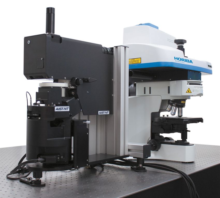
Since its introduction in the early 80’s,
        Scanning Probe Microscopy (SPM) has                   Nano                                               The ultimate versatile platform for
        made nanoscale imaging an affordable
                                                                                                                 physical and chemical characterization
        reality. The technique provides a continuously
        growing variety of surface analysis methods
        for the physical characterization of materials,
        yet label-free chemical sensitivity is still
                                                              RamanTM
        challenging....                                                                                          Powerful
        Raman spectroscopy has long provided
        a versatile way to determine the structure
                                                              Key Features                                         imultaneous SPM and spectroscopic measurements.
                                                                                                                  S
        and chemical composition of molecules and,                                                                High numerical aperture objectives from both top and side for best co-localized spatial resolution
                                                               ULTI-SAMPLE ANALYSIS PLATFORM
                                                              M
        despite its diffraction-limited spatial resolution,                                                        and best TERS collection efficiency.
        has become a standard method in fields                Macro, micro and nano scale measurements can
                                                                                                                   High-throughput and high speed measurements.
        ranging from materials science to the life            be performed on the same platform.
        sciences.                                                                                                   Broad range of detection wavelengths, from deep UV to Infrared.
                                                               ASE OF USE
                                                              E                                                      High spectral resolution with the LabRAM HR Evolution spectrometer.
        In combination, the two techniques                    Fully automated operation, start measuring
        yield an attractive and unique tool                   within minutes, not hours!
        for entering the nano-world.
        With over a decade of experience in this
        exciting new field, we have refined the
                                                               RUE CONFOCALITY
                                                              T                                                                    1                                          2                                          3
                                                              High spatial resolution, automated mapping
        technique to its utmost with uncompromised
        performance to bring you a tool that is not           stages, full microscope visualization options.
        only extremely powerful and versatile,
                                                              HIGH COLLECTION EFFICIENCY
        but is also so easy to use, fast and reliable
        that generating outstanding data is                    Top-down, oblique and bottom Raman detection
        virtually effortless.                                  for optimum resolution and throughput in both
                                                               co-localized and tip-enhanced measurements.
                                                               IGH SPECTRAL RESOLUTION
                                                              H
                                                              Ultimate spectral resolution performance,
                                                              multiple gratings with automated switching,        Enabling feature: IR laser diode           High collection: Wide optical access       Ease of use: Tip replacement
                                                                                                                 for AFM feedback Avoiding Optical          High numerical aperture objectives for     Tip replacement without removing the
                                                              wide spectral range analysis for Raman and
                                                                                                                 Interferences for TERS application         both top and side illuminations            sample or disturbing the optics
                                                              Photoluminescence.
                                                              HIGH SPATIAL RESOLUTION                                             4                                          5                                          6
                                                               Nanoscale spectroscopic resolution (down
                                                               to 10 nm) through Tip-Enhanced Optical
                                                               Spectroscopies (TERS: Tip-Enhanced Raman
                                                               Spectroscopy and TEPL: Tip-Enhanced
                                                               Photoluminescence).
                                                              MULTI-TECHNIQUE / MULTI-ENVIRONMENT
                                                               Numerous SPM modes including AFM,
                                                               conductive and electrical modes (cAFM,
                                                               KPFM), STM, liquid cell and electrochemical       Ease of use: Auto tip-alignment and        Ease of use: XYZ Objective Scanner         Stability: High resonance frequency
            2
                                                               environment, together with chemical mapping       tuning Operator independent, great         Easy Raman laser to tip alignment for      AFM scanners High performance without
                     5                                                                                           reproducibility in tip exchange            long-term stability                        active vibration isolation
3       1                                                      through TERS/TEPL.
                                                               Full control of the two instruments through one
                4                                              workstation and a powerful software control,
                                                               SPM and spectrometer can be operated
                                                               simultaneously or independently.
                                                                                                                 Simple and Fast
                                                               OBUSTNESS / STABILITY
                                                              R                                                     ne-click cantilever alignment, frequency tuning and optimization, requiring no manual adjustments.
                                                                                                                   O
    6
                                                              High resonance frequency AFM scanners,               Easy cantilever exchange without affecting the sample and breaking the alignment.
                                                              operation far away from noises! High                  Fast and intuitive Raman laser to AFM tip alignment with Objective Scanner.
                                                              performance is obtained without active vibration       Full control through one workstation.
                XploRA Nano: OmegaScope AFM combined          isolation.
                     with XploRA Raman microscope
NanoRamanTM Platform AFM-Raman/PL, TERS/TEPL, SNOM, Chemical and Physical Imaging at the Nanoscale - HORIBA
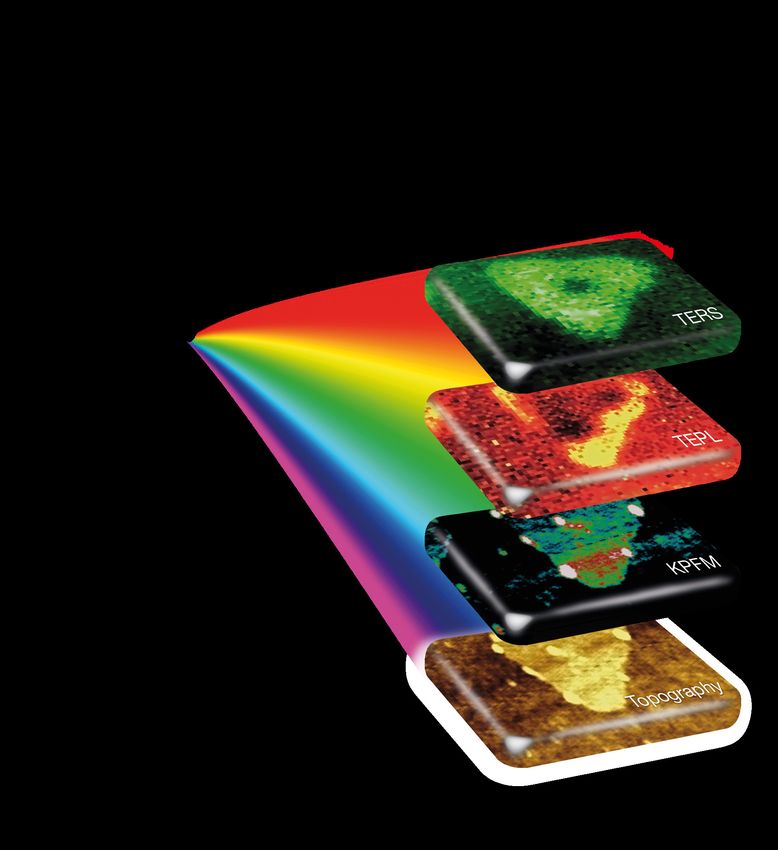
AFM-Raman and TERS made easy

                                                          TERS Tip
                                                                                                                             Reliable AFM-TERS tips
     Reflection
     Configuration       Excitation                                                                                          OmniTM Tip-Enhanced Raman Spectroscopy TERS
                          p
                                                                                                                             probes* are designed to acquire topography and Raman
              Raman                                        Field                                                             spectral information of a sample simultaneously.
            scattering
                                                          Enhancement
                     s                                                                    Tip in contact
                                                                                          Tip retracted
                                                                                                                             The combination of HORIBA's NanoRaman system
        Sample                                                                                                               with OmniTM TERS probes provides the ideal high-
                                                                                                                             enhancement TERS solution. The OmniTM TERS probes
                                                                                                                             are compatible with XploRA Nano, LabRAM HR
                                                                                                                             Nano, LabRAM Soleil Nano, OmegaScope and TRIOS
                                                                                                                                                                                          *Manufactured for HORIBA by APP NANO
                                 Raman       Excitation                                                                      systems. They are nanofabricated using highly doped
                               scattering     p
                                                                                                                            single crystal silicon with unparalleled reproducibility,
                                                                         What is co-localized
                                         s

                                      Transmission                                                                           robustness and sharpness for consistent high resolution
                                      Configuration
                                                                         AFM-Raman?                                          imaging capabilities.

                                                                         Raman and SPM (Scanning Probe Microscope)             i-based AFM tips coated with gold or silver (with
                                                                                                                              S                                                           Multilayer structure: tip optimized to minimize
How TERS works?                                                          analysis can be combined on a single microscope      protective layer)                                            interference from silicon substrate in the spectra
                                                                         system. Co-localized AFM-Raman measurement           Allow all modes of TERS operation: top, side,               Innovative packaging to extend tip shelf life
                                                                         is the sequential or simultaneous acquisition         and bottom optical accesses                                  TERS active layer: silver with protective layer, or
In TERS, the Raman excitation laser       is focused
                                                                         of correlated SPM and Raman maps.                     Suitable for TERS and TEPL measurements with the             gold
at the tip of an SPM probe coated with either gold
or silver . Matching the wavelength of the                               AFM and other SPM techniques like STM                  following lasers: 532, 594, 633, 638, 671, 785, and 830
Raman laser to the natural surface plasmonic                             or tuning-fork Shear-Force or Normal-Force             nm
frequency of the noble metal generates an intense                        microscopy, provide topographic, mechanical,
localized evanescent electromagnetic fied or                             thermal, electrical, and magnetic properties down
«hot spot» at the probe tip . The field extends                          to molecular resolution (on the order of nm, over
only for a few nanometers from the tip surface.                          μm2 area). On the other hand, confocal Raman
Since the intensity of the Raman spectra from                            spectroscopy and imaging provides specific
the sample is proportional to the local electric                         chemical information about the material, with a
field, bringing the hot spot close to the sample
significantly enhances the Raman signal, often by
                                                                         diffraction limited spatial resolution.
                                                                                                                                 TERS proven samples
a power of 105 or 106 .
                                                                                                                                  HORIBA offers a set of test samples: one
                                                                                                                                  is single-wall carbon nanotubes (CNTs)
                                                                                                                                  together with graphene oxide flakes (GO)
                                                                                                                                  suitably dispersed to allow easy imaging.
                                                                                                                                  This sample is used to demonstrate a
                                                                                                                                  routine 20 nm resolution in TERS imaging.

                                                                                                                                  Another sample is dedicated to
                                                                                                                                  demonstration of AFM molecular resolution.

           LabRAM Soleil Nano: OmegaScope AFM, equipped
             with its environmental chamber, combined with
                    LabRAM Soleil Raman microscope
NanoRamanTM Platform AFM-Raman/PL, TERS/TEPL, SNOM, Chemical and Physical Imaging at the Nanoscale - HORIBA
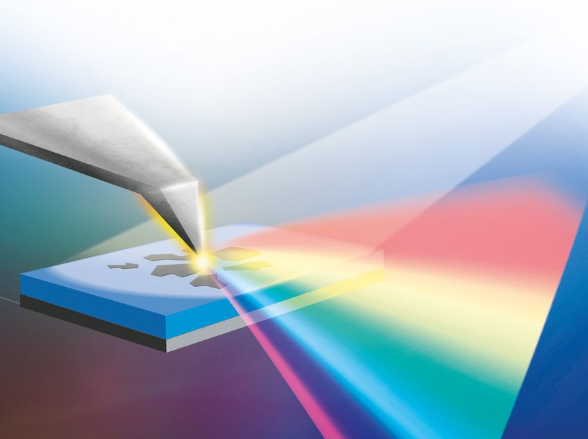
Large area - difficult samples
       Forsterite 1 Forsterite 2 Enstatite
       Whitlockite Anorthite Rhodonite                  Aspirin   Paracetamol   Caffeine   Coating
       Silicon Carbide

1 mm                                                 1 mm                                                                          500 µm                         20 µm                1 µm           6 µm                                         1µm                             1µm

Raman image - Mineral - Macro map                    Raman image - Sectioned pharmaceutical tablet                                 Automatic panoramic AFM       AFM (topography) – 3D Top Mode       AFM (topography) - MFM –                    AFM (topography) – Zinc oxide   AFM (topography) – 150 nm
across a sectioned meteorite                                                                                                       (contact mode) –              imaging - Optical Fiber              Ferrite garnet film                         nanorods - Z range is 3.6 µm    gold nanoparticules
                                                                                                                                   120 scans – CoCr features
                                                                                                                                   on Si surface Sample
                                                                                                                                   courtesy of Dr A.N. Shokin,
                                                                                                                                   NIIFP; Image courtesy of Dr
                                                                                                                                   A. Temiryazev, IRE RAS.

 True confocality - 3D maps                                                                                                                                        High spectral resolution - High selectivity
                                               Quartz CO2 (gas)
  Bead   Matrix                                Water + CO2 (aqueous)                           Emulsion matrix   TiO2 particles                                                                         5L      4L     3L      2L   1L MoS2          cSi   polySi   ncSi              Compressive strain   Tensile strain

10 µm                                        10 µm                                           10 µm                                                                40 µm                               10 µm                                        2 µm                            1 µm

Raman image - XYZ volume map                 Raman image - Fluid inclusion-                  Raman image - Emulsion - Titanium dioxide                           Combined Photoluminescence           Raman image - Layered MoS2                  Raman image - Silicon chip      Raman image - Nano-indented
of expanded polymer bead in                  XYZ volume map through fluid                    particles in emulsion                                               and Raman image - 2D crystal         structure - Map image was                   - crystalline, poly and nano-   silicon – mapping of mechanical
matrix                                       inclusion in a quartz matrix                                                                                        of WS2                               created from low frequency                  crystalline silicon regions     stress
                                                                                                                                                                                                      (
NanoRamanTM Platform AFM-Raman/PL, TERS/TEPL, SNOM, Chemical and Physical Imaging at the Nanoscale - HORIBA
Multi SPM techniques

 9 µm                             3 µm                               2 µm                                1 µm                                1 µm                                  1 µm                                   350 nm                            250 nm

AFM – Bacillus Cereus            MFM - Yttrium Iron Garnet (YIG)    Lateral Force Modulation –          KPFM – DTP (pentacene               Nano Lithography – Vector force       AFM in liquid – Virus like particles   AFM in liquid – plasmid DNA       AFM (height) – DNA origami on
vegetative cells                 film Sample courtesy of Dr A.V.    Polymer-fullerene blend             derivative) on gold                 scratching on polycarbonate           (VLP) Sample courtesy of Prof. O. V.   on mica                           mica –Sample courtesy of Prof.
                                 Maryakhin                          (P3HT:PCBM)                                                                                                   Karpova (Lomonosov Moscow State                                          Michael Norton, Marshall University
                                                                                                                                                                                  University)

  Tip-Enhanced Raman Spectroscopy
                                                                         CH stretching (Polymer)
                                                                                                              CH stretching (Polymer)
                                                                         G band (Graphene)
                                                                                                              G band (Graphene Oxide)
                                                                         2D band (Graphene)

 5 µm                             400 nm                             500 nm                              500 nm                              400 nm                                200 nm

TEPL image – WSe2 flake          AFM and TERS images - Patterned    AFM and TERS images - Circular      TERS image – Graphene oxide on      TERS/TEPL image – MoS2 flake on       TERS/TEPL image – CVD
on Si substrate                  graphene oxide flake by “pulsed-   pattern imprinted in CVD grown      gold                                Si substrate Sample courtesy of Dr    grown WS2 on Si substrate
                                 force lithography”                 graphene transferred to gold                                            Filippo Fabbri (IMEM)                 Sample courtesy of Dr Adam
                                                                                                                                                                                  Schwartzberg (Berkeley Lab)

                                                                                                                                                                                                                           D band (defects)
                                                                                                                                                                                                                           2D band (Graphitic structure)

 600 nm                           800 nm                                                                                                     200 nm
 600 nm                                                              500 nm                              600 nm                                                                    10 nm                                  25 nm

KPFM and TERS images             TERS and AFM images – SAMs of      TERS images - Array of gold         TERS and AFM images – Carbon        TERS image – Gold nanodisks           TERS images – Engineered               TERS image – Single wall carbon
– Graphene Oxide (COOH           azobenzene thiols on gold          disks on Si functionalized with     nanotubes on glass                  (SERS substrate) Sample courtesy of   DNA – (left) A/T and (right) G/C       nanotube on gold – spatial
functionalized) flakes on gold                                      1,4 Aminothiophenol. Sample                                             Dr Jean-François Bryche (Sherbrooke   homopolymeric blocks Data              resolution 8 nm
                                                                    courtesy of Dr Evgeniya Sheremet,                                       University)                           courtesy of Dr Noah Kolodjieski,
                                                                    Technische Universität Chemnitz                                                                               RMD
                                                                                                                                                                                                                                                             Atomic
                                                                                                          True molecular resolution                                                                                                                          resolution

                                                                                                         80 nm                               16 nm                                 22 nm                                  2 nm                              1 nm

                                                                                                        AFM (topography) - Molecular        AFM (topography)- Cholesteryl         AFM (topography) - Palmityl            AFM (topography) - SAMs of        STM (constant current mode) -
                                                                                                        Resolution in Air - Melissic Acid   Stearate on HOPG                      Palmitate on HOPG                      Palmityl Palmitate - the pitch    HOPG
                                                                                                                                                                                                                         between adjacent alkane chains
                                                                                                                                                                                                                         is about 4 Å
     10-6m                                                                     10-7m                                                                        10-8m                                                                             10-9m
                ...Micro...                                                                                                                                                                                      			                      ... To Nanoscopy!
NanoRamanTM Platform AFM-Raman/PL, TERS/TEPL, SNOM, Chemical and Physical Imaging at the Nanoscale - HORIBA
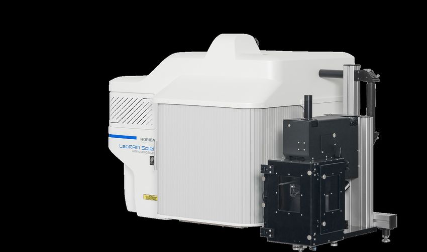
A stable and versatile solution
Integrated Software                                                                                                         CUSTOMER                                       "We are using the NanoRaman platform from HORIBA Scientific
                                                                                                                                                                           for research on carbon-based nanomaterials and especially the
                                                                                                                                                                           characterization of graphene oxide for energy applications. This AFM/

                                                                                                                             STORIES                                       Raman system is easy-to-use with help of the state-of-art hot spot
                                                                                                                                                                           search function and has number of unique build-in SPM techniques,
                                                                                                                                                                           including a unique imaging mode that makes TERS possible. HORIBA
                                                                                                                                                                           (and former AIST-NT) has developed one of the most stable and
NanoRaman data acquisition                                                                                                 A pioneer in TERS
                                                                                                                                                                           versatile scanning probe microscope for the combination with Raman
                                                                                                                                                                           spectroscopy. With the clever, fully motorized and automated instrument

with ONE software                                                                                                          “The NanoRaman team of LPICM lab, Ecole
                                                                                                                           Polytechnique/CNRS, developed jointly with
                                                                                                                                                                           alignment, every advanced measurement at the nanoscale become an
                                                                                                                                                                           easy to configure experiment."

                                                                                                                           HORIBA Scientific the first HORIBA TERS         Prof. Masamichi Yoshimura
                                                                                                                           system prototype a dozen or so years ago.
Key Features
                                                                                                                                                                           Head of the Surface Science Laboratory
                                                                                                                           Later commercialized, the prototype featured    Toyota Technological Institute, Japan
                                                                                                                           STM and AFM SPM modes combined with
                                                                                                                           side illumination in Raman backscattering
  NE SOFTWARE for the acquistion of AFM,
 O                                                                                                                         configuration. Owing to its excellent
 Raman and Photoluminescence signals in
 TERS/TEPL and AFM-Raman/PL co-localized
                                                                                                                           performance and relative ease of use, it was
                                                                                                                           applied with success to the study of various
                                                                                                                                                                           Great technical support
                                                                                                                           materials and nanostructures such as self-      “We have been working for two years on a versatile configuration of
 measurements.
                                                                                                                           assembled organic monolayers, carbon            the NanoRaman platform from HORIBA that allows both reflection and
 LabSpec 6 SPECTROSCOPY SUITE                                                                                             nanotubes, patterned semiconductors,            transmission measurements. As researchers in an electrochemistry Lab,
  for Integrated Multivariate and high level analysis                                                                      etc. Among the outstanding scientific           we were searching for analytical tools which enable the characterization
  at a touch of a button. PCA, MCR, HCA, DCA.                                                                              successes achieved with the system, the         of materials at the nanoscale and under the condition of their operation.
                                                                                                                           world premiere demonstration of stimulated      The stability of the SPM system (true atomic/molecular resolution) and
  NIQUE IMAGING MODES and
 U                                                                                                                         (pump - probe) TERS is to be mentioned.         the robustness of the optical coupling, which enables fast and effective
                                                                                                                           Being quite user-open and versatile, the        TERS mappings, totally met our expectations. The versatility of the Horiba
 processing, including: Spec-TopTM mode -
                                                                                                                           prototype measurement configuration could       system already made possible new characterization pathways such as
 Patented TERS imaging mode: TERS                                                                                          be successfully adapted to accommodate          TERS in liquid and electrochemical TERS. We have also greatly enjoyed
                                                              ULTI-AREA ANALYSIS: Because
                                                             M
 measurement is performed when the tip                                                                                     a polarization control of both excitation and   the technical assistance from Horiba which has definitively boosted our
                                                             full rectangular area scans can be too                        scattered radiations, an external laser pump,
 is in direct contact with the surface, transition                                                                                                                         instrumental developments”.
                                                             time-consuming, several trapezoidal                           as well as an additional detector for Tip-
 between the pixels of the map is performed                                                                                Enhanced Photoluminescence.
                                                             areas can be selected on the AFM image                                                                        Dr. Ivan T. Lucas and Prof. Emmanuel Maisonhaute
 in semicontact mode, which preserves the                                                                                  Since the pioneering years of the TERS          Laboratory “Interfaces and Electrochemical Systems”,
                                                             for Raman mapping.
 sharpness and enhancing properties of the tip.                                                                            prototype, HORIBA Scientific have               Sorbonne University, France
                                                              URVES MAP: Spectroscopic and Force
                                                             C                                                             developed a novel, module-based TERS
  UAL-SPEC MODE: Acquisition of 2 different
 D                                                                                                                         system featuring a large number of SPM
                                                             curves can be performed through images                        modes (STM, AFM, tuning-fork, etc.)
 Raman maps. The far-field-map can be
                                                             characterizing the local stiffness or the                     implementable under various illumination
 subtracted from the near-field-map, giving                                                                                – collection conditions (off-axis, top and
                                                             adhesion distribution. Force constant
 thus a pure TERS image.                                                                                                   bottom backscattering). Thanks to the
                                                             calibration (Sader method).
                                                                                                                           customer-oriented culture of HORIBA, the
                                                                                                                           NanoRaman team of LPICM is currently
                                                                                                                                                                           A fully automated system
                                                                                                                           updating its “historical” prototype with the    With our NanoRaman instrument from HORIBA, we have the full power
                                                                                                                           novel TERS system. It will allow us not         of Raman, AFM, TERS, TEPL, and many other related modes bundled
                                                                                                                           only to pursue our actual research topics       into one system operating in reflection. Every member of my group from
                                                                                                                           by adding new measurements, but also to         bachelor student level to postdoc researcher enjoys the easy usage of
                                                                                                                           initiate new research areas, impossible to      this fully motorized/automated system that can deliver correlated surface
                                                                                                                           address with the present system.“               characterization data from microscale down to nanoscale resolution. We
                                                                                                                                                                           are using this AFM/Raman platform for research on optical and electrical
                                                                                                                           Prof. Razvigor Ossikovski                       properties of nanomaterials every day and we are appreciating the enormous
                                                                                                                           Nano-Raman team leader                          potential of the TERS technique for studying nanomaterials such as CNTs
                                                                                                                           LPICM, Ecole Polytechnique, France              and 2D TMDCs with unprecedented spatial resolution down to 2 nm.
                                                                                                                                                                           Prof. Dietrich R.T. Zahn
                                                                                                                                                                           Head of the Semiconductor Physics Research Group
Multi-area Raman                 Force curves;                     3D topographic image           Spectroscopic curve;                                                     Technische Universität Chemnitz, Germany
mapping (color);                 Adhesion map distribution                                        tip-to-sample distance
background image is                                                                               versus Raman shift
the AFM topography
NanoRamanTM Platform AFM-Raman/PL, TERS/TEPL, SNOM, Chemical and Physical Imaging at the Nanoscale - HORIBA
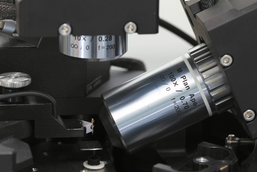
Find out more at www.horiba.com/nanoraman

                                      Worldwide Training and Technical Support
Contact Us
France: Tel. +33 (0)1 69 74 72 00     Jobin Yvon, established in 1819, and now part of the HORIBA Scientific is one of
USA: Tel. +1 732 494 8660
                                      the world's largest manufacturers of analytical and spectroscopic systems and
Japan: Tel. +81(75)313-8121
                                      components.
Germany: Tel. +49 (0) 6251 8475 0
UK: Tel. +44 (0)1604 542 500
                                      The HORIBA Scientific teams are committed to serving our customers with high
Italy: Tel. + 39 06 51 59 22 1
                                      performance products and superior technical support.
China: Tel. +86 (0)21 6289 6060
Singapore: Tel. +65 (0)6 745 8300
Taiwan: Tel. +886 3 5600606           Our staff of experienced application
India: Tel. +91 80 41273637           and service engineers, located around
Brazil: Tel. +55 (0)11 2923 5400      the world, provides full support for your
Other: Tel. +33 (0)1 69 74 72 00      instrument and its future upgrades.
www.horiba.com/scientific
                                      Well equipped application laboratories allow
info.sci@horiba.com
                                      for sample analysis and hands-on training for
Follow Us                             new and experienced users.

                                                                                                    HORIBA Worldwide

                                                                                                                               This document is not contractually binding under any circumstances - Printed in France - ©HORIBA Jobin Yvon 03/2021
                                                                                                     www.ramanacademy.com

                                                                                       Free learning tools for new and
                                                                                       experienced Raman users.
                                                                                       Available to anyone who is interested
                                                                                       in learning more about Raman.

         LabRAM HR Nano: OmegaScope AFM, equipped with its enclosure,
             combined with LabRAM HR Evolution Raman microscope
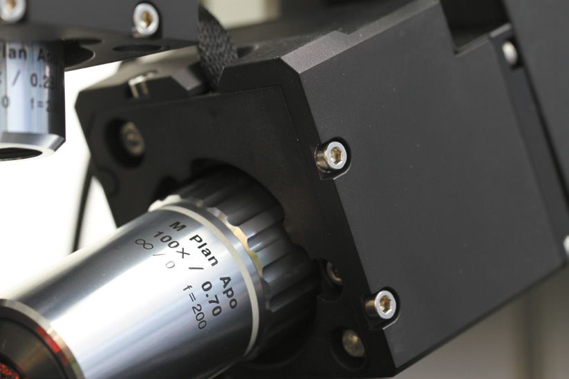
NanoRamanTM Platform AFM-Raman/PL, TERS/TEPL, SNOM, Chemical and Physical Imaging at the Nanoscale - HORIBA NanoRamanTM Platform AFM-Raman/PL, TERS/TEPL, SNOM, Chemical and Physical Imaging at the Nanoscale - HORIBA NanoRamanTM Platform AFM-Raman/PL, TERS/TEPL, SNOM, Chemical and Physical Imaging at the Nanoscale - HORIBA
You can also read