Quantum networks based on color centers in diamond
←
→
Page content transcription
If your browser does not render page correctly, please read the page content below

Quantum networks based on color centers in diamond

                                            Quantum networks based on color centers in diamond
                                                        Maximilian Ruf,1, 2 Noel H. Wan,3, 4 Hyeongrak Choi,3, 4 Dirk Englund,3, 4, 5, a) and Ronald Hanson1, 2, b)
                                                        1) QuTech, Delft University of Technology, PO Box 5046, 2600 GA Delft, The Netherlands
                                                        2) KavliInstitute of Nanoscience Delft, Delft University of Technology, PO Box 5046, 2600 GA Delft,
                                                        The Netherlands
                                                        3) Department of Electrical Engineering and Computer Science, Massachusetts Institute of Technology, Cambridge,
                                                        Massachusetts 02139, USA
                                                        4) Research Laboratory of Electronics, Massachusetts Institute of Technology, Cambridge, Massachusetts 02139,
                                                        USA
                                                        5) Brookhaven National Laboratory, Upton, New York 11973, USA

                                                        (Dated: 11 May 2021)
                                                        With the ability to transfer and process quantum information, large-scale quantum networks will enable a suite of
                                                        fundamentally new applications, from quantum communications to distributed sensing, metrology, and computing. This
arXiv:2105.04341v1 [quant-ph] 10 May 2021

                                                        perspective reviews requirements for quantum network nodes and color centers in diamond as suitable node candidates.
                                                        We give a brief overview of state-of-the-art quantum network experiments employing color centers in diamond, and
                                                        discuss future research directions, focusing in particular on the control and coherence of qubits that distribute and store
                                                        entangled states, and on efficient spin-photon interfaces. We discuss a route towards large-scale integrated devices
                                                        combining color centers in diamond with other photonic materials and give an outlook towards realistic future quantum
                                                        network protocol implementations and applications.

                                               With the Panama-Pacific International Exposition of 1914             I. A BRIEF INTRODUCTION TO QUANTUM
                                            fast approaching, AT&T’s leadership grew increasingly                   NETWORKS
                                            alarmed: it was still impossible to hold a coast-to-coast tele-
                                            phone call, despite the company touting it for years. The es-              In a future quantum network (see Fig. 1), remote parties
                                            sential problem “was a satisfactory telephone repeater,” re-            are connected by sharing long-lived entangled states3,4 . Ar-
                                            called an AT&T senior manager from conversations with the               guably, the most promising way of linking distant nodes is to
                                            company’s chief engineer John J. Carty1 . Whereas mechani-              employ fiber- or free-space photonic communication channels
                                            cal repeaters adequately boosted voice signals on the metro-            to establish entanglement. While all photon-based schemes
                                            scale, they added so much noise that signals quickly became             are associated with losses that scale with distance5 , motivat-
                                            unintelligible over longer distances. A fundamentally new re-           ing the need for quantum repeaters6 , heralding entanglement
                                            peater technology was needed. Tasked with this urgent mis-              generation on successful photon transmission events maps
                                            sion, Bell Laboratories developed the “audion” trion vacuum             these losses into reduced entanglement generation rates with-
                                            tube, just in time for the 1914 Exposition. Over the ensuing            out lowering entanglement fidelities7–9 .
                                            decades, the triode made way to the transistor, copper wires               Optically-mediated remote entanglement of individually
                                            yielded to optical fiber, and binary digits (”bits") became             controllable qubits has been generated for different materi-
                                            the universal language of information, transcending physical            als platforms, including quantum dots10,11 , trapped ions12–14 ,
                                            modality. Today, as the authors edit these sentences over a             neutral atoms15–18 , and nitrogen-vacancy centers in dia-
                                            globe-spanning video conference, the world is at the cusp of            mond19,20 . Other promising systems, including so-called
                                            the next information revolution, as quantum bits (”qubits")             group-IV defects in diamond 21–24 , defects in SiC25–27 , and
                                            have become the universal units fueling a new generation of             rare-earth ions in solid-state hosts28–30 , show great potential
                                            ‘quantum information technologies’. And once again, an es-              for quantum network applications, although remote entangle-
                                            sential challenge is to develop a “satisfactory repeater” – this        ment has not yet been generated. Another less explored ap-
                                            time, capable of relaying (but not amplifying!2 ) quantum in-           proach is to link distant superconducting quantum processors
                                            formation signals. This article reviews the progress towards            using coherent conversion of microwave photons to telecom
                                            one such “quantum repeater” as well as other quantum net-               frequencies31–35 .
                                            work technology using color centers in diamond to connect
                                                                                                                       Apart from fundamental tests of physics20 , small-scale
                                            quantum information among spins and photons.
                                                                                                                    quantum networks have been used to demonstrate key net-
                                                                                                                    work protocols such as non-local quantum gates17 , entan-
                                                                                                                    glement distillation36 , and very recently entanglement swap-
                                                                                                                    ping37 . These networks are currently limited to a few nodes37 ,
                                                                                                                    distances of up to one kilometer20 , and entanglement genera-
                                                                                                                    tion rates in the Hz to kHz regime10–16,19,20 . A major chal-
                                                                                                                    lenge for the coming decade is to transition from the current
                                                                                                                    proof-of-principle experiments to large-scale quantum net-
                                                                                                                    works for use in fields such as distributed quantum computa-
                                            a) Electronic   mail: englund@mit.edu                                   tion38,39 , quantum enhanced sensing40,41 , and quantum secure
                                            b) Electronic   mail: r.hanson@tudelft.nl                               communication42 .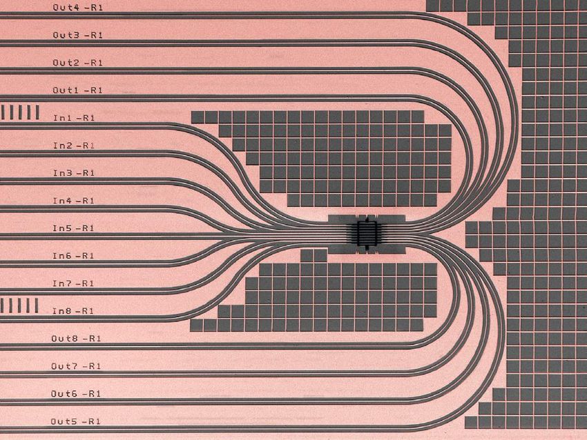
Quantum networks based on color centers in diamond                                                                                                 2

    Quantum                                                                                                                Quantum enhanced
  communication                                                                                                                 sensing

 Networked quantum                                                                                                                  Unknown
    computation                                                                                                                    applications

                                                                                                                                   ? ?
FIG. 1. Schematic overview of a future large-scale quantum network, consisting of nodes containing optically interfaced qubits (purple) with
long coherence times. Photons routed via optical fibers or free-space channels serve as mediators to create entanglement (blue wiggled lines).
Local area and trunk backbone quantum repeaters (dark and light red circles, respectively) are used to enable a high entanglement generation
rate over large distances, overcoming photon transmission loss. The entanglement generation is heralded, meaning that detection of certain
photon statistics signals the successful generation of an entangled state that is available to a network user for further processing and applications
such as networked quantum computation, quantum secured communication, quantum enhanced sensing, and potential not yet discovered tasks.

   In this perspective article, we focus on color centers in di-             (at telecommunication wavelengths for fiber-based systems),
amond as potential building blocks for large-scale quantum                   to establish remote entanglement at high rates. Second, the
networks. We identify their strengths and challenges, current                ability to store quantum states during entanglement genera-
research trends, and open questions, with a focus on qubit                   tion; in particular, this requires qubit coherence times under
control, coherence, and efficient spin-photon interfaces. We                 full network activity to be longer than the time it takes to gen-
lay out a path towards large-scale, integrated devices, and dis-             erate entanglement between nodes. Third, the capability to
cuss possible protocols and functionalities such devices could               store several entangled states per node with a capability for
enable.                                                                      high-fidelity operations between them, to enable multi-qubit
   This article is organized as follows: Sec. II introduces the              protocols such as error correction.
requirements for the nodes of a quantum network and gives                       Color centers in diamond satisfy most of these require-
a high-level overview of why color centers in diamond are                    ments, and have enabled some of the most advanced experi-
promising candidates to meet these demands. We then give                     mental demonstrations of quantum network protocols to date.
a brief overview of state-of-the-art quantum network experi-                 We here give a concise, high level overview of the achieved
ments employing color centers in diamond in Sec. III, to give                and projected key capabilities of color centers in diamond [see
the reader a sense of the current research status. In Sec. IV, we            Fig. 2(a)], motivating a detailed treatment (and also including
introduce the physics behind color centers in diamond, to un-                the relevant literature) in the remains of this article:
derstand their strengths and challenges for quantum network
applications in the remainder of this article. Sec. V discusses                  1. The color center contains an individually controllable,
open questions regarding the coherence and control of nuclear                       optically active spin (communication qubit), with ac-
spin memory qubits surrounding color centers in diamond that                        cess to several long-lived nuclear spins (memory qubits)
can be used as additional quantum resources. In Sec. VI, we                         in its surrounding. These memory qubits can be ma-
outline the need and strategies for an enhancement of the spin-                     nipulated with high fidelity to free up the communica-
photon interface of diamond color centers and discuss promis-                       tion qubit and enable multi-qubit protocols. They have
ing future research in this direction. Sec. VII outlines a path                     a long coherence time enabling robust state storage dur-
towards large-scale, integrated diamond devices that may en-                        ing subsequent network activity.
able future quantum network experiments with high rates. Fi-
nally, Sec. VIII concludes by illuminating possible applica-                     2. The internal level structure is suited to generate remote
tions for future quantum networks.                                                  entanglement. In particular, color centers feature spin-
                                                                                    state-selective optical transitions that can entangle the
                                                                                    color center’s spin state with a photonic state, e.g. in
                                                                                    the number / polarization / time basis (see Fig. 2(b).)
II. REQUIREMENTS FOR A QUANTUM NETWORK
NODE                                                                             3. Optical emission of color centers is bright and can be
                                                                                    collected with high efficiency, enabling high entangle-
   To make a material platform suitable for a node in a quan-                       ment generation rates. This emission is in the visible to
tum network in which entanglement is mediated by photons,                           near-IR spectrum, and thus at wavelengths that are as-
it has to fulfill three main requirements4 . First, the capability                  sociated with higher fiber transmission losses than for
to interface at least one qubit efficiently with optical photons                    photons in the telecom band. However, it is possible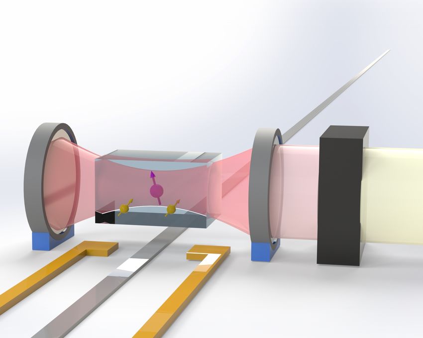
Quantum networks based on color centers in diamond                                                                                         3

                      (a)                                                                        (b)
                                                                                                       ES

                                                                                                                 X
                                                                                                       GS

FIG. 2. Overview of a quantum network node based on color centers in diamond and simplified optical level scheme. (a) Schematic of a
quantum network node in diamond, consisting of an optically-active (communication) qubit (purple) embedded between two highly reflective
mirrors (an optical cavity) to enhance the interaction strength of photons with the qubit. The state of the color center qubit can be swapped
onto long-lived nuclear spin (memory) qubits in the surroundings (orange) using high fidelity gates that employ microwave or RF pulses
delivered via dedicated lines (gray). Tuning of network nodes to an optimal frequency operation point is e.g. enabled by applying a static
electric field via electrodes (yellow). Frequency-conversion (black box) can be used to down-convert photons entangled with the state of the
communication qubit to telecommunication wavelengths, for which photon transmission losses are low. The color center features spin-resolved
optical transitions between an optical ground (GS) and excited state (ES), enabling optically-mediated remote entanglement generation (b).

      to efficiently convert this emission to the telecom band          here) used a single-photon scheme43 yielding fidelities ∼ 82%
      while maintaining quantum correlations.                           at rates of ∼ 10 Hz37 .
                                                                           Importantly, these schemes generate entanglement in a her-
   4. Diamond is a solid-state material, potentially enabling           alded fashion, making the fidelity robust to photon loss and
      nanophotonic device fabrication at a large scale. Such            the generated entangled states available for further use. In
      devices can also be integrated with photonic circuits,            the vicinity of the NV center, a 13 C nuclear spin is used as
      and efficient interfacing of color centers embedded in            a memory qubit at the middle node, coupled to the NV cen-
      such systems has been demonstrated.                               ter electron spin via the hyperfine interaction. The nuclear
                                                                        spin is controlled via tailored microwave pulses applied to the
                                                                        NV center spin44 that simultaneously decouple the NV elec-
III. STATE OF THE ART OF DIAMOND-BASED                                  tron spin from the other nuclear spins. Characterization of
QUANTUM NETWORKS                                                        the nuclear spin environment of an NV center has enabled
                                                                        communication qubit coherence times above one second45 . In
   Two recent experiments showcasing the potential of color             addition, entangled states have been stored in 13 C memory
centers in diamond as quantum network node candidates                   qubits for up to ∼ 500 subsequent entanglement generation
can be seen in Fig. 3, together defining the state of the art           attempts37,46,47 . Combined with the demonstrated capabil-
in quantum networks. Fig. 3(a) shows a laboratory-scale                 ity of entanglement distillation (generating one higher fidelity
quantum network based on nitrogen-vacancy (NV) centers in               state from two lower fidelity states)36 and deterministic entan-
diamond37 . Three NV centers in separate cryostats, linked via          glement delivery (by generating entanglement between two
optical fiber channels in a line configuration, are operated as         nodes faster than it is lost, albeit not under full network ac-
independent quantum network nodes. The centers are set to               tivity)43 , these experiments highlight the potential of the NV
a common optical emission frequency via electric field tuning           center as a quantum network node. As we discuss in detail
(DC Stark shift)19 . The network is used to demonstrate dis-            below, a main challenge for the NV center is the low fraction
tribution of three-partite Greenberger-Horne-Zeilinger (GHZ)            of emitted and detected coherent photons, limiting the entan-
entangled states across the nodes, as well as entanglement              glement rates.
swapping to achieve any-to-any connectivity in the network37 .             Recently, a new class of defect centers in diamond has also
This network sets the state of the art for entanglement-based           gathered the attention of the community: the family of group-
quantum networks.                                                       IV color centers in diamond, of which the negatively charged
   Entanglement between the nodes is generated using a                  silicon-vacancy (SiV) center is the most studied member.
photon-emission-based scheme, in which spin-photon entan-               Fig. 3(b) shows a schematic of a SiV center embedded in a
glement is locally generated at each NV node using mi-                  photonic crystal cavity, which increases the interaction of light
crowave and laser pulses. The photonic modes are then in-               with the communication qubit as compared to emission in a
terfered on a beam splitter, thereby erasing the which-path             bulk diamond material (discussed in Sec. VI below). Spin-
information. Subsequent photon detection heralds the genera-            photon entanglement with fidelity ≥ 94 % has been generated
tion of a spin-spin entangled state between two NV nodes19,43 .         in this system using cavity quantum electrodynamics (cQED)
Early experiments19 had employed two-photon entangling                  reflection-based schemes, in which photons impinging on the
schemes reaching fidelities ∼ 90%20 at ∼ mHz rates. More re-            cavity containing the communication qubit are reflected or
cent experiments (including the three-node network discussed            transmitted depending on the spin-state of the communica-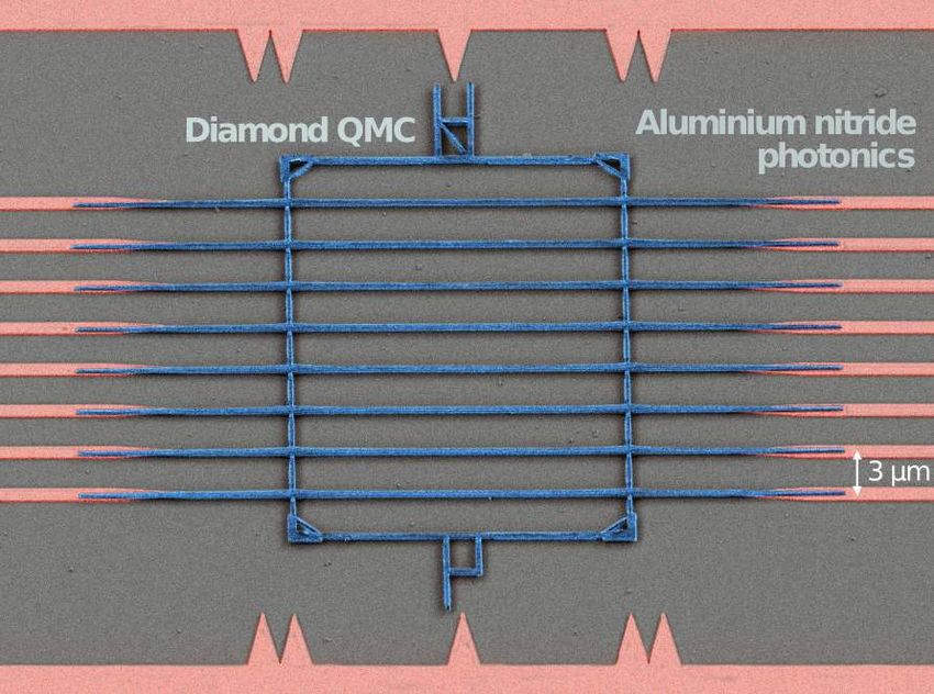
Quantum networks based on color centers in diamond                                                                                                  4

 (a)                                    Communication qubit                   (a)                  (b)                 (c)

                                                                                 C
                           Alice                                                       N
           Lab 2                                                                                           IV
                                                   Memory qubit
                                                                                       V

           Long-distance       30 m
           entanglement

                                                                              FIG. 4. Schematic atomic structure of NV (a) and group-IV (b) color
             Lab 1
                                                                              centers in diamond and ground state level structure of group-IV color
                                                           Bob                centers (c). The inversion symmetry of group-IV color centers leads
                                           2m                                 to a vanishing permanent electric dipole moment, making those de-
                                                   Optical fiber              fect centers suitable for integration in nanophotonic structures. This
                     Charlie                       connection                 structure also results in orbital and spin double degeneracy in the
                                                                              ground and excited state (c, only ground state shown for simplicity)
(b)                                                                           that is lifted by (mostly) spin-orbit coupling (∆gs ) and by application
 (a)                                                               T=100 mK
                                                                              of an external magnetic field (B), respectively. Phonon-induced tran-
                               Si
                                13                                            sitions (γ+ / γ− ) between orbital states limit (communication) qubit
                                    C
                                                                              coherence times (see text).

                                                                              centers and other closely related group-IV color centers as
 (b)                                                                          nodes for a quantum network (see Sec. VI).
FIG. 3. State-of-the-art experiments showing the potential of color
centers in diamond as quantum network nodes. (a) Schematic of a
3-node quantum network based on nitrogen-vacancy (NV) centers in
diamond, linked with optical fibers. One of the network nodes fea-            IV. OPTICAL AND SPIN PROPERTIES OF COLOR
tures a 13 C nuclear spin that is used as a memory qubit to store (part       CENTERS IN DIAMOND
of) an entangled state and free up the communication qubit, while
subsequent entanglement is created using this communication qubit a
second time. Figure from 37 , reprinted with permission from AAAS.               Nitrogen-vacancy and group-IV color centers in diamond
(b) Schematic of a silicon-vacancy (SiV) center (blue circle) embed-          feature different structural symmetries, which result in differ-
ded in a fiber-coupled (dark grey) all-diamond photonic crystal cavity        ent properties of their spin-photon interface. Here, we briefly
(light grey area with holes). Coherent emitter-cavity cooperativities         introduce the most important differences between those color
∼ 100 have enabled high-fidelity reflection-based spin-photon entan-          centers in diamond, to the point necessary to understand cur-
glement generation23 , and control of individual 13 C nuclear spins           rent limitations and research directions described in the re-
via microwave pulses applied to the electron spin of the silicon va-          mains of this article; we refer the reader to the many excellent
cancy spin qubit (yellow electrodes) has been demonstrated48 . Fig-
                                                                              articles that cover the physics of these color centers in great
ure adapted with permission from Ref.48 . Copyright (2019) by the
American Physical Society.
                                                                              detail57–59 . In this article, we consider all color centers to be in
                                                                              the negative charge state, except where indicated differently;
                                                                              this negative charge state is the one most commonly studied
                                                                              and used in experiments geared towards entanglement gener-
tion qubit48 . While entanglement between distant SiV cen-                    ation.
ters has not yet been demonstrated, strong collective interac-                   Fig. 4 shows the difference in atomic structure of nitrogen-
tions between two SiV centers49 in the same cavity and prob-                  vacancy (NV) centers and group-IV color centers (con-
abilistic entanglement generation between two SiVs 50,51 in                   sisting of silicon-vacancy (SiV)54,65,66 , germanium-vacancy
one waveguide have been observed. In addition, photon out-                    (GeV)70 , tin-vacancy (SnV)24,71 and lead-vacancy (PbV)75
coupling efficiencies from the emitter-cavity system into fiber               centers). An NV center is formed by a nitrogen atom replac-
> 0.9 have enabled the demonstration of memory-enhanced                       ing a carbon atom of the diamond lattice, next to a lattice va-
quantum communication23 . This experiment sets the state of                   cancy, giving rise to a C3v symmetry [Fig. 4(a)]. The NV
the art for quantum repeater experiments.                                     center possesses a permanent electric dipole moment, making
   Additionally, recent experiments have demonstrated key                     the optical transition frequencies sensitive to charge fluctua-
quantum network node capabilities, including dynamical de-                    tions in its environment57 . This sensitivity to electric fields
coupling of the SiV spin from the bath with coherence times                   has been used as a resource to tune different NV centers onto
above 1 ms22,52 , 13 C nuclear spin initialization, control, and              resonance80 , counteracting local strain inhomogeneities in the
readout via the central SiV electron spin53,54 , and frequency                host diamond crystal which shift the transition frequencies of
control of SiV centers via strain tuning51,55,56 . Combined                   color centers. However, it has also hindered the nanophotonic
with recent efforts to fabricate SiV centers in nanophotonic                  integration of NV centers due to degradation of their optical
waveguides at a large scale and their integration in photonic                 properties near surfaces81,82 .
circuits56 , these results show the potential of silicon-vacancy                 The NV center features an outstanding spin energy relax-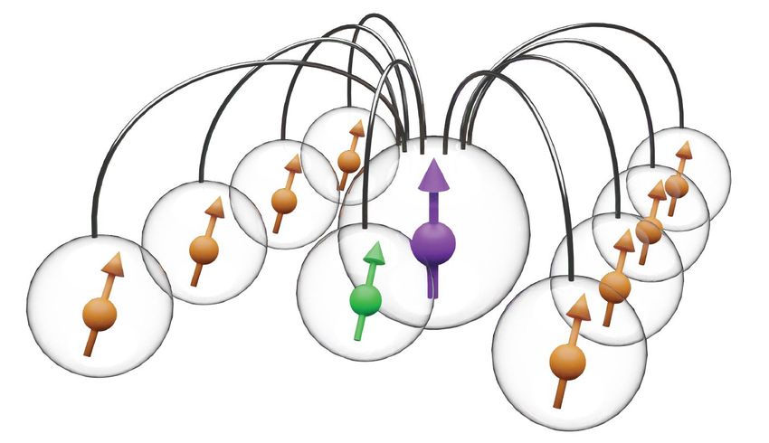
Quantum networks based on color centers in diamond                                                                                               5

           Vacancy        ZPL                Quantum          Debye-Waller        Radiative         Ground state splitting       Toper
                     wavelength [nm]      efficiency [%]         factor          Lifetime [ns]            [GHz]                   [K]
             SiV          73723        (1 − 10)50,60 / 6061 (0.65 − 0.9)62,63       1.750,64               5064–66                0.1
            GeV           60267           (12 − 25)68,69         ∼ 0.670         (1.4 − 6)21,67             17070                 0.4
             SnV         62024,71             ∼ 8071              0.5772        (4.5 − 7)24,73,74         85024,71                1.8
             PbV          52075             not known           not known            > 375                 570075                 9.8
             NV           63757               > 8576            0.0377,78       (11 − 13)47,77,79      not applicable        not applicable

TABLE I. Overview of optical and orbital properties of group-IV (SiV, GeV, SnV, PbV) and NV defect centers in diamond. All listed numbers
are approximate values. We consider all defects to be in the negative charge state. The Debye-Waller Factor characterizes the fraction of
radiative emission into the ZPL, while we define the quantum efficiency as the ratio of radiative to all decay. Ground state splitting denotes
splitting between orbital states in the optical ground state of group-IV color centers (see Fig. 4(c) and text). Toper is the calculated operation
temperature below which the expected orbital lifetime is above 100 ms. We estimate this temperature by calculating the phonon transition rate
γ+ ∝ ∆3gs /(e(∆gs/kb T ) − 1) [see Fig. 4(c)], where ∆gs is the orbital ground state splitting, T is the temperature, and kB the Boltzmann constant
(as γ− > γ+ , γ+ determines the qubit coherence times), as in Refs.24,71 . We then find the proportionality factor to map this to a concrete
temperature by using the measured values of Ref.66 .

ation time of over 8 h83 . Quantum states have been stored in               ties for coherent SiV control are a result of qubit dephasing
the NV center’s electronic spin for over one second by decou-               during microwave pulses, as relatively low Rabi frequencies
pling the electron from unwanted interactions in its environ-               (∼ 10 MHz) are used to limit heating-induced decoherence.
ment using tailored microwave pulse sequences45 . Fidelities                It is expected that the use of superconducting waveguides87
in quantum networks experiments have reached > 0.99% for                    will further improve microwave pulse fidelities (as a result of
single qubit gates and ∼ 98% for two-qubit gates (between                   potentially significantly reduced ohmic heating) for all color
NV electron and 13 C nuclear spins) 37 .                                    centers.
   For group-IV color centers, the group-IV atom takes an in-                  Spin dephasing in the group-IV qubit subspace is domi-
terstitial lattice site between two lattice vacancies. The result-          nated by phonon-assisted transitions to the upper ground state
ing inversion-symmetric D3d structure of the defect [Fig. 4(b)]             orbital branch, which leads to the acquisition of a random
results in no permanent electric dipole and thus a first-order              phase: while the phonon transitions are in principle spin-
insensitivity to electric field fluctuations. As a consequence,             conserving, the detuning between the spin states varies de-
tuning optical transition frequencies of group-IV color cen-                pending on which orbital state is occupied, see Fig. 4(c)88,89 .
ters by electric fields is relatively inefficient84,85 , potentially        In Tab. I, we map reported ground state splittings into a con-
necessitating other techniques (discussed in Sec. VI below).                crete performance metric by extrapolating the temperatures
On the other hand, the vanishing permanent electric dipole                  Toper below which we expect an orbital coherence time > 100
makes these color centers excellent candidates for integration              ms due to low phonon occupation. From this, we see that a
into photonic nanostructures (also discussed in Sec. VI be-                 larger ground state splitting (associated with stronger spin-
low).                                                                       orbit coupling strengths for heavier ions) is beneficial for
   Group-IV emitters also feature a different level structure               maintaining long qubit coherence. However, this requires
than the NV center: both optical ground and excited states are              higher microwave driving powers for similar off-axis strain
formed by doubly-degenerate orbital states, which are each                  values, as the strain-induced orbital mixing is related to the
split into pairs by spin-orbit interaction and the Jahn-Teller              spin-orbit coupling strength, and thus the overlap between or-
effect. Under an external magnetic field, the double spin de-               bital states is reduced54 . All-optical spin control schemes rep-
generacy in each pair (S = 1/2) is lifted58,65,86 . The qubit               resent an alternative to microwave driving, as demonstrated
subspace can then for example be defined over the two op-                   e.g. for SiV64,90,91 and GeV70 centers. For SnV centers, spin
posing spin sublevels of the optical ground state’s lower or-               initialization by optical pumping has been observed24 . An-
bital branch [see Fig. 4(c)]. This, however, means that direct              other way of defining and driving a qubit could be to mix
microwave driving of the qubit levels is forbidden in first or-             the (mostly) orthogonal spin components via an off-axis mag-
der, as one would need to flip both spin and orbital quantum                netic field, and use surface acoustic waves to drive phonon
numbers. Typically, this complication is overcome by work-                  transitions between the orbital levels, with demonstrated Rabi
ing with emitters with transversal strain ∼ ∆gs , which mixes               frequencies ∼ 30 MHz92 . Such an off-axis magnetic field,
the orbital levels, such that the qubit state can be effectively            however, is at odds with achieving the high spin cyclicity
described by the spin only and thus be driven with higher                   needed for single shot spin state readout and high fidelity en-
efficiency54 . Coherent microwave control of group-IV color                 tanglement generation, necessitating a careful tradeoff54 . For
centers has recently been demonstrated for SiV centers52,54 ,               magnetic fields aligned with the color center’s symmetry axis,
with infidelities on the percent level52 . For other group-IV               readout fidelities above 99.99% have been achieved48,52 .
color centers, only incoherent microwave driving of spin tran-                 Tab. I also shows a comparison of the most important op-
sitions has been achieved so far24,70 . The reported infideli-              tical properties for both group-IV color centers and nitrogen-
Quantum networks based on color centers in diamond                                                                                 6

vacancy centers in diamond. To generate entanglement, only               (a)
the fraction of coherent photons emitted in the zero-phonon-
line (ZPL, for which no lattice vibrations assist the tran-
sition57 ) can be used19 . Importantly, all quantified
                                                  e        zero-                                      e
phonon-line emission fractions for group-IV color centers are
                                       14
                                         N as the inversion
significantly larger than for the NV center,                                                14
                                                                                              N
symmetry of these emitters causes their excited states C
                                                     13 to have
                                                                                                           C
                                                                                                          13
greater overlap with the optical ground state86 , resulting in a
higher fraction of direct photon transitions93,94 . While most
recent quantum memory experiments with SiV centers have
operated in dilution refrigerators (see below) in order to sup-          (b)
press thermal phonon population52,91 , the SnV center with                14

relatively high expected operating temperature requirements
might be particularly promising for use as quantum network
node. We note that the neutral charge state variants of group-
IV color centers are also promising, as they potentially com-
bine the favorable spin-photon interface of negative group-
IV color centers with the excellent spin coherence times and
easy qubit manipulation of negative nitrogen vacancy cen-
ters86,95–98 . We do not discuss it extensively here due to its
early stage of study.

                                                                                 14

V.   ENHANCING THE MEMORY QUBITS
                                                                   FIG. 5. State-of-the-art research for increasing memory qubit num-
   We now discuss the state of the art and future research di-     bers and control for color centers in diamond. (a) Schematic
                                                                   overview of a local 10-qubit quantum register in diamond, formed
rections regarding the memory qubits of color centers in di-
                                                                   from a nitrogen-vacancy center (purple), a native 14 N nuclear
amond. The most common isotope of carbon is 12 C. How-             spin, and 8 surrounding 13 C nuclear spins. (b) Connection map
ever, the 13 C isotope with natural abundance of about 1.1%        of the spin register in (a), demonstrating entanglement genera-
carries a nuclear spin of 1/2. In the past decade, techniques      tion between all pairs of qubits in the register. Figure adapted
have been developed (mostly on NV-based systems) to con-           with permission from Ref.99 , in accordance with creativecom-
trol these nuclear spins via the position-dependent hyperfine      mons.org/licenses/by/4.0/legalcode.
coupling. Universal nuclear spin control using electron de-
coupling sequences that are on resonance with a single 13 C
spin has been demonstrated 44 . This has enabled the demon-        spin qubits [see Fig. 5(top)] that allow entangled state genera-
stration of coherence times above 10 seconds, and electron-        tion between all pairs of qubits [Fig. 5(bottom)], creation of a
nuclear gate fidelities ∼ 98% for individual 13 C spins in NV-     local 7-qubit GHZ state, as well as memory coherence times
based systems36,99 . Additionally, up to one memory qubit per      of single and two qubit states of over ten seconds99 . This re-
communication node has been used in an NV-based quantum            sult (achieved on a similar device as used for distant entan-
network setting to date36,37 . For the case of SiV centers (and    glement generation19,36,37 ) shows that it is realistic to expect
group-IV color centers in general), on the other hand, the spin-   diamond-based quantum nodes containing many qubits in the
half nature of the system leads to a vanishing first-order sen-    near-term future. Such registers could enable scalable, modu-
sitivity of decoupling sequences to individual 13 C hyperfine      lar quantum computation38 and universal, fault-tolerant error
parameters, thus requiring long decoupling times (and / or po-     correction44,100–102 . Additionally, we expect that RF driving
tentially off-axis magnetic fields that are at odds with a high    of nuclear spins will overcome current limitations in manipu-
spin cyclicity of optical transitions) to isolate out single nu-   lating nuclear spins for group-IV color centers, as the nuclear
clear spins. So far, electron-nuclear gate fidelities have been    spin transition frequencies depend on the hyperfine parame-
limited to ∼ 59% for SiV centers48 ; 13 C nuclear spins close      ters on first order in this case54 . Overcoming issues related
to group-IV color centers have not yet been used in quantum        to sample heating and background amplifier noise could then
networks experiments.                                              also enable to address multiple nuclear spins simultaneously,
   A first area of research is thus to extend the number of        thus reducing decoherence associated with long gate times99 .
available nuclear spin qubits per network node, as well as         Additionally, cross-talk between nuclear spins, as well as un-
their control speeds and fidelities. Recently developed gate       wanted coupling to other spins could be reduced when us-
schemes based on interleaving radiofrequency (RF) driving of       ing the full information of the environment of a color cen-
13 C nuclear spins (to control previously unaddressable qubits)    ter103 (potentially acquired while involving automated tech-
with dynamical decoupling pulses (to decouple from the spin        niques104 ) to simulate and tailor gate sequences for a specific
bath) have allowed the creation of a local quantum register of     spin environment, and computationally optimizing them for
an NV communication qubit and up to 9 surrounding nuclear          overall protocol fidelity. Another way of extending the num-
Quantum networks based on color centers in diamond                                                                                   7

ber of controllable nuclear spin qubits per node is to also em-       A.   Strategies for enhancing the spin-photon interface
ploy the nuclear spin of a nuclear spin containing color center
atom isotope, e.g. of 14 N (nuclear spin of 1)105 or 29 Si (nuclear      The two most common strategies to enhance the spin-
spin of 1/2)66 .                                                      photon interface are by increasing the photon flux at the detec-
   A second research direction is to increase the coherence           tor through improvements in photon collection, and through
time per available memory qubit under full network activ-             cavity or Purcell enhancement, which increases light-matter
ity (in particular entanglement generation). The "always-on"          interaction and spontaneous emission rates (see Fig. 6). Here,
nature of the hyperfine interaction of 13 C nuclear spin mem-         we only give a brief overview of these methods, and refer to
ory qubits and the NV center has limited memory coherence             the many extensive diamond-color-center specific review arti-
in quantum networks to ∼ 500 entanglement generation at-              cles that cover them in detail, see e.g. Refs.59,115–117 .
tempts37,47 . Uncontrolled electron dynamics, which result for
instance from control infidelities and stochastic electron spin
initialization during an entangling sequence, cause dephas-           1.   Collection efficiency enhancement
ing of the nuclear spin memory qubits47 . Techniques such as
higher magnetic fields at the color center location can speed            A common method to enhance collection efficiency from
up gate times and shorten the entanglement generation ele-            color centers in diamond is to fabricate dome-shaped solid im-
ment, thus reducing the time over which random phases can be          mersion lenses around the emitters [Fig. 6(a)], which leads to
picked up37,47 . Additionally, decoupling pulses on the mem-          a higher fraction of light being collected, as total internal re-
ory qubits that suppress quasi-static noise in the environment        flection is avoided by the light striking the diamond surface
have shown initial promise to prolong nuclear memory qubit            at a perpendicular angle. These devices have been used to
coherence under network activity for NV centers47 . Other             increase emission from NV118–122 , SiV64,65 , and GeV70,123
promising routes to extend the nuclear spin memory coher-             centers; all diamond-based remote entanglement generation
ence time involve reducing the color center’s state-dependent         experiments reported to date have used these devices, with
coupling strength (the main dephasing channel), e.g. by em-           detection efficiencies of emitted photons of up to ∼ 10%120 .
ploying decoherence-protected subspaces (formed from two                 A second class of collection efficiency enhancement meth-
or more individual spins, or pairs of strongly-coupled spins          ods is based on nanostructures that modify the far-field emis-
that mostly cancel the state-dependent hyperfine interaction          sion of a dipole emitter. These structures comprise different
term)45,46,106 , and using isotopically purified samples for          dimensions, designs, and supported wavelength ranges, and
which weakly coupled 13 C nuclear spin qubits can be con-             include parabolic reflectors124,125 [Fig. 6(b)], nanopillars126 ,
trolled107,108 ). Other methods are to engineer systems of cou-       nanowires127,128 , nanocones129 , gratings130,131 and diamond
pled defects (e.g. involving a 13 C nuclear spin qubit coupled        waveguides21,50,56,132–137 [Fig. 6(c)]. While they offer large-
to a P1 center in the vicinity of an NV center109 , or to use         scale fabrication and higher collection efficiencies than solid
the nitrogen nuclear spin of a second NV center (whose ni-            immersion lenses (reported dipole-waveguide coupling effi-
trogen nuclear spin is used as a memory) in proximity to the          ciencies above 55%56,125 ), the demands in nano-fabrication
communicator NV center110,111 .                                       and color center placement are more stringent than for solid-
                                                                      immersion lenses, and emitters have to be brought in close
                                                                      proximity to nano-fabricated surfaces. This proximity to sur-
                                                                      faces is believed to be the cause of optical instability for some
VI.   ENHANCING THE SPIN-PHOTON INTERFACE                             diamond color centers, as discussed in detail below. Such in-
                                                                      stabilities make it challenging to produce indistinguishable
   Optically-mediated entanglement generation with high               photons from remote centers as required for entanglement
rates requires quantum network nodes with efficient spin-             generation 138,139 .
photon interfaces. However, the relatively high refractive in-
dex of diamond (∼ 2.4) leads to significant total internal re-
flection at the diamond-air interface, which limits photon col-       2.   Purcell enhancement
lection efficiencies. Entanglement rates are further reduced
by the finite fraction of photons emitted into the zero-phonon           Another way of enhancing the spin-photon interface is to
line (ZPL) that can be used for entanglement generation (see          embed the dipole emitter inside an optical cavity, making use
Sec. IV above). Thus, techniques that can increase the fraction       of the Purcell effect, described by a Purcell factor FP . This
of collected photons at ZPL wavelengths, and / or increase            factor scales with the ratio of the cavity quality factor, Q (in-
the interaction of light with the emitter are required. Here,         versely proportional to the cavity’s energy decay rate), to the
we discuss both strategies, as well as their suitability for en-      cavity mode volume, V (describing the cavity light field con-
hancing the spin-photon interface of different diamond color          finement)113 . Briefly, a cavity enhances the density of states
centers, and the state of the art and future avenues for this re-     around its resonance frequency, such that the spontaneous
search. We note that strong light-matter interactions also open       emission of an embedded dipole emitter is increased when on
the door to entangling schemes alternative from the photon-           resonance with the cavity following Fermi’s golden rule. Ad-
emission-based protocols discussed above7,8 , e.g. based on           ditionally, the cavity funnels emitted light into a well-defined
spin-dependent cavity reflections9,23,112–114 .                       mode that can be readily matched e.g. to that of optical fibers.
Quantum networks based on color centers in diamond                                                                                                                    8

(a)                                      (b)                                                         quantifies the ratio of coherent decay into the cavity mode to
                                                                                                     undesired decay, and is given as117,145

                                                                                                                               4g2              γhom
                                                                                                                 Ccoh =                   =C             .          (2)
                                                                                                                          κ(γhom + γdep )    γhom + γdep

                                                     2 μm                                            Ccoh can be interpreted as the probability of coherent atom-
                                 10 μm
                                                                                                     photon interaction, and plays an important role in the fidelity
(c)                                                                                                  and efficiency of many near-deterministic quantum protocols
                                                                                                     (which require Ccoh  1)145 .
                                                       2 μm
                                                                                                        To date, cavity enhancement of diamond color centers
(d)                                  (e)                                                             has been demonstrated for different implementations, in-

                                                                        Closed-cycle Cryostat (4K)
                                                       Fused Silica
                                                                                                     cluding diamond-on-insulator whispering gallery mode res-
                                                            Mirror                                   onators77,146 and nanodiamond plasmonic antennas147 . An-
                                           ~ μm       Diamond                                        other class of devices are based on the coupling of non-
                                                                                                     diamond resonators to color centers in nanodiamonds148–151
                                                                                                     or diamond films152–154 . Open and tunable micro-cavities
                                                                                                     geometries have also been demonstrated for embedded nan-

                                                              Piezo
 1 μm                                      Fiber                                                     odiamonds155–160 and thin diamond membranes68,78,79,161,162
                                                                                                     [Fig. 6(d)].        Steady progress in diamond nanofabrica-
                                                                                                     tion has also led to all-diamond photonic crystal cavi-
FIG. 6. Devices used to enhance the spin-photon interface of color
centers in diamond. Solid immersion lenses120 (a), parabolic re-
                                                                                                     ties23,48–50,54,81,163–167 [Fig. 6(e)], with demonstrated coherent
flectors124 (b, adapted with permission from Ref.124 . Copyright                                     cooperativities exceeding 100 for the case of the SiV center23 .
(2017) American Chemical Society.), and waveguide (c, SEM im-
age of device from the same chip used in Ref.137 ) allow to en-
hance photon collection efficiencies from embedded color centers,                                       Quantum network applications also require the efficient
compared to emission in a bulk host material. Photonic crystal140                                    coupling of light from these nanostructures to optical fibers.
[d, Figure adapted with permission from Ref.141 , copyright by The                                   Different methods of coupling to fiber-based communication
Optical Society (OSA)] and open, tunable micro-cavities79 (e, Fig-                                   channels have been realized to date, including optimized free-
ure adapted with permission from Ref.79 , in accordance with cre-                                    space couplers with efficiencies up to ∼ 25%137,168 , notch
ativecommons.org/licenses/by/4.0/legalcode) enhance collection ef-                                   couplers with efficiencies ∼ 1%50 , grating couplers with ef-
ficiency, while modifying the nanophotonic environment at the same
                                                                                                     ficiencies ∼ 30%146,169 , and double-136,170,171 and single-
time. This allows to additionally enhance the number of photons                                      23,49,54,172 sided fiber-tapers with efficiencies of up to ∼ 90%.
emitted at a certain wavelength via the Purcell effect, compared to
collection enhancement tools.

                                                                                                     B.   Looking forward: key challenges and potential solutions
A commonly used parameter to quantify the radiative emis-
sion enhancement by the cavity (defined as the ratio of the                                             Having introduced different theoretical concepts to increase
dipole-cavity emission, γcav , compared to the emission in a                                         the spin-photon interface of color centers in diamond, we now
homogeneous medium, γhom = γrad + γnonrad ) is the coopera-                                          discuss the experimental state of the art of such enhancement,
tivity, C, defined as                                                                                highlighting key challenges and potential research directions.
                       4g2    γcav
                 C=         =      = FP β0 η,                         (1)
                      κγhom   γhom
                                                                                                     1.   NV centers
where g is the dipole-cavity coupling rate, κ is the energy de-
cay rate from the cavity, γrad is the free-space radiative emitter                                      While the nitrogen-vacancy (NV) center has been a
decay rate, γnonrad is the non-radiative emitter decay rate, β0                                      workhorse of quantum network demonstrations with color
is the fraction of photon emission from the emitter into the                                         centers in diamond, its low fraction of optical emission at the
zero-phonon line (given by the Debye-Waller factor), and η is                                        zero-phonon line (ZPL) frequency of 3%, as well as limited
the quantum efficiency (defined as the ratio of radiative to all                                     collection efficiency from solid immersion lenses currently
decay). While this quantifies the efficiency of the spin-photon                                      restrict local entanglement generation rates to
Quantum networks based on color centers in diamond                                                                                   9

research, and that recent experiments geared at understand-        2.   Group-IV color centers
ing the effect and origins of surface noise on the NV center
spin173 , and the local electrostatic environment of NV cen-          The first-order electric field insensitivity of group-IV
ters174 show promise towards understanding the causes of sur-      color centers in diamond24,67,73,75,86,137,186–188 has enabled
face charge noise. Combined with proposals for active optical      the demonstration of close-to-lifetime limited optical tran-
driving to reduce spectral diffusion effects175 , this could re-   sitions even in heavily fabricated nanophotonic struc-
vive the field of NV centers in nanophotonic structures in the     tures21,50,54,56,137,187 . To date, photonic crystal cavity cou-
future.                                                            pling of group-IV color centers in diamond at low tempera-
   The challenge imposed by nearby surfaces can be circum-         tures has been demonstrated for SiV23,48–50,54 and SnV cen-
vented by embedding microns-thin diamond membranes be-             ters74 , with demonstrated Ccoh > 100 for the case of the SiV
tween two highly reflective mirrors176 . A recently reported       center23 . This system allows for spin-state dependent photon
fabrication technique has formed NV centers with bulk-like         reflection, enabling high fidelity single shot spin state read-
optical properties in µm-thin diamond membranes that can           out with demonstrated fidelities > 99.9% [see Fig. 7(c,d)].
be embedded in such cavities via a combination of electron         This has recently enabled the first demonstration of memory-
irradiation, high temperature annealing, and a tailored dia-       enhanced quantum communication23 .
mond etching sequence82 [Fig. 7(a)]. This has allowed for             A key requirement for many remote entanglement gener-
the first demonstration of resonant excitation and detection of    ation schemes is the ability to tune two group-IV color cen-
optically coherent NV centers, Purcell enhanced by an optical      ters located on separate chips to a common resonance fre-
cavity79 , as would be required for cavity-enhanced entangle-      quency. So far, tuning the emission frequency of group-IV
ment generation. However, the Purcell enhancement in this          emitters has been demonstrated using strain51,55,56,89,189 , elec-
experiment was limited to ∼ 3, (mostly) due to cavity-length       tric fields84,85 , and Raman-type50,190 schemes (although the
fluctuations ∼ 100 pm induced by a closed-cycle cryocooler.        latter is only compatible with emission-based entanglement
Previously, it has been shown (using off-resonant excitation)      generation schemes), but only for single emitters, or several
that Purcell enhancement factors of up to 30 (correspond-          emitters in one structure. The first two tuning techniques de-
ing to 46% of light emitted in the ZPL) can be achieved for        form the orbitals of the group-IV color centers, and thus the
such open micro-cavities in a liquid helium bath cryostat (fea-    color’s inversion symmetry is broken, leading to an observed
turing lower cavity length fluctuations)78 [Fig. 7(b)]. Com-       increase in transition linewidths and spectral diffusion under
bined, these experiments demonstrate that there is a near-term     applied external strain / electric field (potentially due to an in-
path from the current Ccoh ∼ 0.1 towards Ccoh ∼ 1 and co-          crease in sensitivity to charge noise in the environment). We
herent photon collection efficiencies ∼ 10%. In addition, re-      note that recent experiments indicate a larger tuning range of
cent results suggest that it should be possible to reach the       transitions for strain tuning (as compared to electric field tun-
required pm-scale cavity length fluctuations even in closed-       ing) for the same induced line broadening56,84,85 .
cycle cryostats30,177 , which would remove the need for a liq-        While close-to-lifetime limited linewidths of group-IV
uid helium infrastructure at each quantum network node.            color centers in nanophotonic structures have been observed,
   Another active area of research is to create shallow, stable    experiments still routinely show spectral shifts and charge in-
NV centers178–180 at controlled locations; both the electron       stabilities, leading to broadening ∼ several lifetime-limited
irradiation technique employed in Ref.79 , as well as recently     linewidths49,54,56,137 , as well as large local strain fields. While
introduced laser-writing techniques181 can form optically co-      dynamic strain tuning can be used to suppress slow spectral
herent NV centers, but rely on native nitrogen in the sample       diffusion (seconds timescale)51 , it is challenging to improve
to recombine with introduced lattice vacancies and thus miss       the homogeneous linewidth (sub-microsecond timescale) that
precise control of the site of NV center formation. However,       enters the coherent cooperativity using this approach. Typi-
for maximal Purcell enhancement, NV centers should be posi-        cally, emitters are created by high-energy implantation, fol-
tioned at an antinode of the cavity field. While such precision    lowed by a high temperature annealing step to form group-IV
can be achieved using ion implantation, recent research has        vacancy centers and to reduce the effects of lattice damage
shown that NV centers created via this technique suffer from       from the implantation process183 . However, there is evidence
increased optical linewidths compared to NV centers formed         that even such high temperature treatments can not fully re-
during growth182 , even after extended high temperature treat-     cover the original diamond lattice182 . A recently developed
ments to restore the diamond lattice183 .                          promising method to overcome this limitation employs low
   While it will remain challenging to achieve coherent coop-      energy shallow ion implantation, combined with overgrowth
erativites  1 (and thereby enter the near-deterministic spin-     of diamond material191 . Another strategy could be to com-
photon interface regime145 ), the open cavity approach is pro-     bine low-density ion implantation with electron irradiation, to
jected to speed up current emission-based entanglement gen-        reduce the amount of damage created in the lattice via the
eration schemes by ∼ 2 orders of magnitude79 . This could          (heavy) ion implantation192 . Combined with controlled engi-
allow for continuous deterministic entanglement generation         neering of the diamond Fermi level96,193,194 , these techniques
(generating high fidelity entanglement faster than it is lost),    could increase the quality and stability of group-IV color cen-
and enable experiments such as the formation of a quan-            ter optical transitions49,54,56,73,75,137 .
tum repeater surpassing direct transmission184 , and device-          Another area of active development involves the design
independent quantum key distribution185 using NV centers.          and fabrication of the nanophotonic structures. Despite re-
Quantum networks based on color centers in diamond 10
Microwave Striplines
(a) (b) ZPL2
104 τR = 7.06 ns
Counts in 1000 s
Height (μm)
40
44.7 μm
20
0
103
τR = 10.4 ns
0 10 20 30 40
500 μm
Time (ns)
(c) f0 (d) 0.6
1.00
Count rate (kHz)
20
Cavity reflection
Probability
0.75 0.4
10
0.50
0.2 0
0 20 40
0.25 Time (seconds)
0.00 0.0
-1 0 1 0 7 10 20 30
Laser detuning (GHz) Number of photons in 30 μs
FIG. 7. State-of-the-art research for enhancing the spin-photon interface of color centers in diamond for quantum networks applications. (a)
Confocal microscope image of a typical µm-thin etched diamond sample containing NV centers with bulk-like optical properties, bonded via
Van-der-Waals forces to a mirror containing microwave striplines. Location and direction of a sample height trace measurement is indicated
with a red arrow. Such samples have recently enabled the first demonstration of resonant excitation and detection of coherent Purcell enhanced
NV centers79 . Figure adapted with permission from Ref.82 , further permissions related to the material excerpted should be directed to the
American Chemical Society. (b) NV center excited state decay in the ZPL for different emitter-cavity detunings for an NV center in an open
micro-cavity under pulsed off-resonant excitation. Inset shows normalized decay curves. Figure adapted with permission from Ref.78 , in
accordance with creativecommons.org/licenses/by/4.0/legalcode. (c) Spin-state dependent reflection spectrum of a SiV center in a critically
coupled photonic crystal cavity with Ccoh ∼ 100. The spin-state dependent photon reflection with high collection efficiency enables spin-
state readout with fidelity > 99.9 % in a single shot (d), and has recently enabled the first demonstration of memory-enhanced quantum
communication23 . Figures (c) and (d) are adapted with permission from Ref.23 .
cent progress195,196 , growing high quality, thin film dia- the fabrication parameter space is somewhat less explored for
mond on large scales is challenging, and (to the best of the latter technique).
our knowledge) there is no wet processing technique that
Currently, all listed fabrication methods routinely achieve
can etch bulk single-crystal diamond along its crystal planes,
photonic crystal cavity quality factors ∼ 104 , about two or-
thus requiring either laborious thinning of diamond on a
ders of magnitude lower than simulated values209 . These de-
low index material, or sophisticated techniques to produce
viations are caused by a combination of surface roughness54 ,
suspended, wavelength-thick diamond devices. While ini-
non-uniform hole sizes74 , and deviations from the expected
tial research focused on creating sub-µm-thin diamond films
device cross-section210 ; we expect that an order-of-magnitude
via selectively wet-etching a localized graphitized diamond
improvement in device quality factors is within reach upon
layer197–202 or etching down a super-polished thin diamond
further optimization. Furthermore, although photonic crystal
membrane61,81,163,164,203 , these methods typically feature low
nanocavities can be designed and fabricated to resonate at the
device yield (as a consequence of challenges in device han-
ZPL frequency, they are especially sensitive to process vari-
dling and initial material thickness variations). Thus, recent
ations, leading to a resonance wavelength spread of ∼ 5 nm
research has focused on fabricating structures directly in com-
across devices209 . Nonetheless, this spread in frequency may
mercially available bulk diamond material via a combination
be overcome by cavity tuning methods50,81,212 , which are in
of a hard mask and an angled diamond etch (leading to a
any case needed for the precise overlapping of the ZPL and
triangular device cross-section)50,54,132,140,204–206 , or a quasi-
cavity frequency.
isotropic (dry) undercut etch, which selectively etches along
certain diamond crystal planes (leading to rectangular device As nanofabrication methods are constantly refined, it is also
cross-section)56,168,207–211 . Known limitations to these pro- likely that current methods of optimally aligning color centers
cesses include mixing of TE- and TM-like modes that will ul- within nanophotonic structures (to guarantee maximal over-
timately limit device quality factors for triangular devices, as lap between the optical mode and the dipole emitter) can be
well as a relatively high bottom surface roughness for quasi- further improved. Towards this end, various methods have
isotropic etched devices (although it is worthwhile to note that already been demonstrated, including the targeted fabrication
around pre-located centers124 , or ion implantation into devicesQuantum networks based on color centers in diamond 11
using either masks54 or focused implantation50,56 . Compared decade. The first notable feature of PICs for quantum tech-
to the SiV center for which Ccoh ∼ 100 has been demonstrated, nologies is their compact footprint, which not only promotes
GeV and SnV centers have intrinsically higher radiative ef- dense integration, but also reduces phase errors in quantum in-
ficiencies and thus potentially higher cooperativities, which terference of photons222 . Next, phase modulators in PICs can
may increase cavity-QED-based protocol fidelities (see dis- implement on-chip switches for routing photons within an op-
cussion below). tical network222 , and material nonlinearities can be used for
We note that group-IV color centers in diamond are also efficient frequency conversion between visible and telecom-
suitable for integration into tuneable, open micro-cavities, as munication photons231 . Finally, multi-channel optical access
recently demonstrated for GeV68 and SiV161,162 centers at can be accomplished using standard fiber arrays, and electri-
room temperature. It should be possible to achieve Ccoh
1 cal packaging for large-scale control of color centers can be
for these systems, potentially providing a viable alternative to achieved using potential metal layers in a PIC stack.
the more fabrication-intensive nanostructures. Photonic circuits in diamond have been previously demon-
strated for opto-mechanics169 and nonlinear optics232 . Gal-
lium phosphide-on-diamond photonics have also been used to
VII. TOWARDS LARGE-SCALE QUANTUM NETWORKS route the emission from NV centers154 . However, the non-
deterministic creation and integration of color centers in de-
Having discussed the core quantum network components vices, as well as the absence of single-crystal diamond wafers
based on diamond color centers, we now turn to what is re- have limited the scale of diamond integrated photonics (see
quired to build these into a network capable of distributing Sec. VI). One way to combine the functionalities and per-
entanglement over large distances at high rates. formance of industry-leading photonic circuits with diamond
First, a future quantum internet will likely make use of ex- is through heterogeneous integration of diamond with other
isting fiber infrastructure. This necessitates the matching of material systems. Also known as "hybrid photonics"233,234 ,
the photon wavelength from the network node to the telecom- this approach is akin to modern integrated circuits in that dis-
munication bands using quantum frequency conversion. Re- crete chips are separately optimized and fabricated and then
cently, it has been demonstrated that spin-photon entangle- populated into a larger circuit board. Examples of hetero-
ment can be preserved after frequency down-conversion of a geneous integration include modulators and lasers in silicon
∼ 637 nm photon entangled with the spin-state of the NV cen- photonics235 . In the context of quantum photonics, recent suc-
ter to telecommunication wavelengths (∼ 1588 nm)215 . Simi- cesses include quantum emitters233,234 and single-photon de-
lar conversion techniques can be applied to other color centers tectors236 , which are otherwise difficult to achieve in a single
and quantum systems216–220 . Future work will focus on in- material platform with high performance.
creasing the system efficiency and potentially integrating on- Heterogeneous integration of diamond color centers with
chip conversion (see below). PICs circumvents the yield issues associated with all-diamond
Second, future quantum networks covering large distances architectures, thereby allowing potentially many addressable
will require many quantum repeater stations –– each with a qubits within a single chip. A recent result showing the
large number of qubits –– for multiplexing, purification and large-scale integration of color centers in diamond with hy-
error-correction. For example, 5-10 repeater stations with brid photonic integrated circuits56 is shown in Fig. 8(a-c). Di-
kilohertz entangled bit (ebit) rates need a total of O(108 ) data amond quantum micro-chiplets, each consisting of 8 diamond
qubits to reach mega-ebits per second communication221 . Al- nanophotonic waveguides with at least one addressable group-
though color center devices are already produced using stan- IV color center, are integrated with PICs based on aluminum
dard nanofabrication techniques, the needed scale for high- nitride [Fig. 8(c)]. After fabrication using the quasi-isotropic
rate, high-fidelity networks would require large-scale manu- undercut technique (see Sec. VI), a total of 16 chiplets num-
facturing of quantum nodes. This task not only entails qubit bering to 128 waveguides were positioned with sub-microns
and device production but also the packaging of efficient op- accuracy on the PIC [Fig. 8(a)] using a pick-and-place tech-
tical and microwave signals to and from many independent nique [Fig. 8(b)]. The coupling of the color center to the
color centers at once. waveguide can be as high as 55 %, and the diamond-PIC cou-
Optical technologies such as photonic integrated circuits pling and PIC-to-optical fiber coupling are reported to be 34 %
(PICs) may play an important role in addressing these chal- and 11 %, respectively. In addition, electrodes in this hybrid
lenges. Their programmability222 and access to a large num- PIC enabled the in-situ tuning of optical transition frequencies
ber of spatial modes223 are especially of interest to quantum within this integrated device architecture56 . The availabil-
network applications. Similar to their bulk optics counter- ity of multiple color centers per waveguide potentially allows
parts, PICs comprise of low-loss on-chip components, such as for spectral multiplexing237,238 , which is a hardware-efficient
waveguides, filters and switches. References222–225 review the path to multiplying the total number of qubits to Ns × N f ,
device concepts and state of the art of PIC technologies that where Ns and N f are the number of spatial and frequency
may be relevant to quantum network applications. Driven by channels, respectively.
foundry adoption, as well as new frontiers in data communi- With further improvements in waveguide-emitter coupling
cation226,227 , photonic processors228,229 and optical quantum as well as diamond-nanocavity integration with PICs, such
computing230 , integrated photonic circuits have advanced dra- a hybrid architecture could become an important building
matically in manufacturability and complexity over the last block of future quantum network nodes. Looking forward,You can also read