Semiconductors: U.S. Industry, Global Competition, and Federal Policy - October 26, 2020 - Federation of American Scientists
←
→
Page content transcription
If your browser does not render page correctly, please read the page content below
Semiconductors: U.S. Industry, Global
Competition, and Federal Policy

October 26, 2020

                              Congressional Research Service
                               https://crsreports.congress.gov
                                                      R46581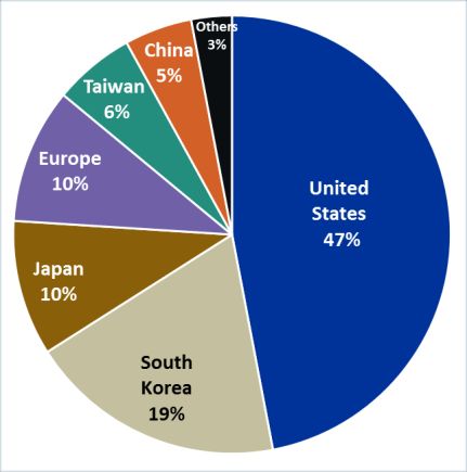
SUMMARY

                                                                                                       R46581
Semiconductors: U.S. Industry, Global
                                                                                                       October 26, 2020
Competition, and Federal Policy                                                                        Michaela D. Platzer
Semiconductors, tiny electronic devices based primarily on silicon or germanium, enable nearly         Specialist in Industrial
all industrial activities, including systems that undergird U.S. technological competitiveness and     Organization and Business
national security. Many policymakers see U.S. strength in semiconductor technology and
fabrication as vital to U.S. economic and national security interests. The U.S. semiconductor          John F. Sargent Jr.
industry dominates many parts of the semiconductor supply chain, such as chip design.                  Specialist in Science and
Semiconductors are also a top U.S. export. Semiconductor design and manufacturing is a global          Technology Policy
enterprise with materials, design, fabrication, assembly, testing, and packaging operating across
national borders. Six U.S.-headquartered or foreign-owned semiconductor companies currently
operate 20 fabrication facilities, or fabs, in the United States. In 2019, U.S.-based semiconductor    Karen M. Sutter
manufacturing directly employed 184,600 workers at an average wage of $166,400.                        Specialist in Asian Trade
                                                                                                       and Finance
Some U.S.-headquartered semiconductor firms that design and manufacture in the United States
also have built fabrication facilities overseas. Similarly, U.S.-headquartered design firms that do
not own or operate their own fabrication facilities contract with foreign firms located overseas to
manufacture their designs. Much of this overseas capacity is in Taiwan, South Korea, and Japan,
and increasingly in China. Some Members of Congress and other policymakers are concerned that only a small share of the
world’s most advanced semiconductor fabrication production capacity is in the United States. Other have become
increasingly concerned about the concentration of production in East Asia and related vulnerability of semiconductor supply
chains in the event of a trade dispute or military conflict and other risks such as product tampering and intellectual property
theft.

Some Members of Congress and other U.S. policymakers have expressed concerns about the economic and military
implications of a loss of U.S. leadership in semiconductors. China’s state-led efforts to develop an indigenous vertically
integrated semiconductor industry are unprecedented in scope and scale. Many policymakers are concerned that these efforts,
if successful, could significantly shift global semiconductor production and related design and research capabilities to China,
undermining U.S. and other foreign firms’ leading positions. Although China’s current share of the global industry is still
relatively small and its companies produce mostly low-end chips, China’s industrial policies aim to establish global
dominance in semiconductor design and production by 2030. Moreover, Chinese semiconductor competencies could support
a range of technology advancements, including military applications. Another issue for policymakers is how to address
competing interests: China is an important market for U.S. semiconductor firms but U.S. and foreign industry are helping to
advance China’s capabilities. China’s government outlays (an estimated $150 billion to date) and its role as a central
production point for global consumer electronics are generating strong incentives and pressures on U.S. and foreign firms to
focus on China. The Chinese government views access to foreign capabilities in the near term as a key pathway to accelerate
China’s indigenous development. Also of concern to many are China’s state-led efforts to acquire companies and access
semiconductor technology through both licit and illicit means; targeted intellectual property (IP) theft; and technology-
transfer pressures.

Issues before Congress include the appropriate role of government in assisting U.S. industry; how best to focus federal
financial assistance; the amount of funding each proposed activity would need to accomplish its goals for sustaining U.S.
semiconductor competitiveness; how to coordinate and integrate federal activities internally and with initiatives of the U.S.
semiconductor and related industries; and how to address China’s ambitious industrial plans, trade practices of concern, and
the role of U.S. firms in China’s emerging semiconductor market. Legislation has been introduced in the 116th Congress to
increase federal funding for semiconductor research and development efforts; collaboration between government, industry,
and academic partners; and tax credits, grants, and other incentives to spur U.S. production. Two bills under consideration are
the Creating Helpful Incentives to Produce Semiconductors (CHIPS) for America Act (S. 3933/H.R. 7178) and the American
Foundries Act (AFA) of 2020 (S. 4130). Some of the provisions of these acts have been included in other bills.

Congressional Research Service
Semiconductors: U.S. Industry, Global Competition, and Federal Policy
Contents
Introduction ..................................................................................................................................... 1
Semiconductor Industry Basics ....................................................................................................... 2
Semiconductor History and Technological Challenges ............................................................. 4
Wafer Size ........................................................................................................................... 5
Feature Size......................................................................................................................... 6
The Global Semiconductor Industry ............................................................................................... 6
Semiconductor Market Segments .................................................................................................... 8
Global Semiconductor Production .................................................................................................. 9
Materials Used for Wafer Manufacturing................................................................................ 10
Design; Fabrication; and Assembly, Testing, and Packaging ................................................... 11
Design ............................................................................................................................... 12
Fabrication: Facilities (Foundries) .................................................................................... 14
Fabrication: Equipment and Other Suppliers .................................................................... 15
Assembly, Testing, and Packaging .................................................................................... 17
Key Parts of the Global Semiconductor Supply Chain ........................................................... 17
Global Semiconductor Fabrication Capacity .......................................................................... 18
The U.S. Semiconductor Manufacturing Industry......................................................................... 18
Industry R&D Spending .......................................................................................................... 19
Semiconductor Manufacturing Jobs ........................................................................................ 19
Semiconductor Production in the United States ...................................................................... 20
The Global Semiconductor Landscape .......................................................................................... 23
East Asia .................................................................................................................................. 24
China ....................................................................................................................................... 26
U.S. Controls on Semiconductors ..................................................................................... 31
Europe ..................................................................................................................................... 34
The Federal Role in Semiconductors ............................................................................................ 35
Current Federal R&D Efforts to Develop Potential Technology Alternatives and
Supplements to Semiconductors .......................................................................................... 36
National Security Concerns ........................................................................................................... 39
DOD Trusted Foundry Program .............................................................................................. 40
Current Semiconductor-Related Legislation ................................................................................. 43
Concluding Observations .............................................................................................................. 44
Figures
Figure 1. Semiconductors: An Enabling Technology ...................................................................... 3
Figure 2. Evolution of Silicon Wafer Size ....................................................................................... 5
Figure 3. Worldwide and U.S. Semiconductor Industry Sales ........................................................ 7
Figure 4. Global Semiconductor Industry Market Share, by Sales, 2019 ....................................... 7
Figure 5. Typical Global Semiconductor Production Pattern ........................................................ 10
Figure 6. Integrated Circuit End-Use Markets and Estimated Growth Rates................................ 13
Congressional Research ServiceSemiconductors: U.S. Industry, Global Competition, and Federal Policy
Figure 7. U.S. Exports to China, Share of U.S. Exports to the World of Semiconductor
Fabrication Equipment ............................................................................................................... 16
Figure 8. Revenue for Value Chain Segments by Headquarters Location, 2018........................... 17
Figure 9. Semiconductor Industry Market Share, by Sales, 2019 ................................................. 24
Tables
Table 1. Semiconductor Fabrication Capacity ............................................................................... 18
Table 2. Top 10 States in Semiconductor Manufacturing Employment ........................................ 20
Table 3. 300mm (12-inch) Semiconductor Fabs in the United States, 2019 ................................. 22
Table 4. Worldwide 300mm Semiconductor Fab Count................................................................ 26
Table 5. Examples of Abandoned or Blocked Chinese Semiconductor Transactions ................... 32
Table B-1. The Top 15 Semiconductor Suppliers Worldwide ....................................................... 50
Appendixes
Appendix A. History of the Federal Role in Semiconductor Development and
Competition ................................................................................................................................ 47
Appendix B. Top 15 Semiconductor Suppliers Worldwide ........................................................... 50
Appendix C. Semiconductor-Related Legislation in the 116th Congress ...................................... 51
Contacts
Author Information........................................................................................................................ 53
Congressional Research ServiceSemiconductors: U.S. Industry, Global Competition, and Federal Policy
Introduction
Semiconductors, tiny electronic devices based primarily on silicon or germanium, are a uniquely
important enabling technology. They are fundamental to nearly all modern industrial and national
security activities, and they are essential building blocks of other emerging technologies, such as
artificial intelligence, autonomous systems, 5G communications, and quantum computing. For
more than six decades, consistent growth in semiconductor capabilities and performance and
concurrent cost reductions have boosted U.S. economic output and productivity and enabled new
products, services, and industries.
Since the immediate post-World War II era, the United States has been a global leader in the
research, development, design, and manufacture of semiconductors. The United States remains a
leader in semiconductor research and development (R&D), chip design, and some aspects of
semiconductor manufacturing, but a complex mix of both U.S. and foreign companies makes up
the semiconductor supply chain, including fabrication facilities, or fabs. Nevertheless, in 2019,
the United States accounted for 11% of global semiconductor fabrication capacity, down from
13% in 2015, continuing a long-term decline from around 40% in 1990.1
Many policymakers see the competitiveness of the U.S. semiconductor industry, including
domestic production of semiconductors and the retention of manufacturing knowledge, human
expertise, and hands-on experience, as vital to U.S. economic and national security interests.2
Several factors contribute to congressional concerns about the competitiveness of the U.S.
semiconductor industry:
Sustaining the ability of the industry to continually improve semiconductor
performance while decreasing cost through technological innovation.
Because semiconductors are integral components in almost all industrial activity
and fundamental to several emerging technologies, their performance and price
affect multiple sectors and the broader U.S. economy.
Retaining and growing high-skilled and high-paying semiconductor industry
jobs in the United States. Semiconductor manufacturing jobs in the United
States pay twice that of the average U.S. manufacturing job.
The movement of many U.S. firms toward a “fabless” business model. In this
model, fabless semiconductor and related firms focus on R&D and design
capabilities, while contracting with outside, mostly foreign, fabrication
companies.3 This fabless trend has contributed to a concentration of global chip
production among a handful of firms operating fabs in East Asia.
U.S. reliance on global supply chains and production concentrated in East
Asia and vulnerability to disruption or denial due to trade disputes or
1 By 2019, Taiwan, South Korea, and Japan accounted for two-thirds of the world’s semiconductor fabrication capacity,
and China for 12% of global fabrication.
2 Executive Office of the President, President’s Council of Advisors on Science and Technology, Report to the
President: Ensuring Long-Term U.S. Leadership in Semiconductors, January 2017, at
https://obamawhitehouse.archives.gov/sites/default/files/microsites/ostp/PCAST/pcast_ensuring_long-
term_us_leadership_in_semiconductors.pdf. Also, see Senate floor debate on the National Defense Authorization Act
for Fiscal Year 2021, Congressional Record, vol. 166, part 128 (July 21, 2020), p. S. 4325.
3 Beginning in the 1980s, some semiconductor companies began to contract for their fabrication needs rather than
maintaining their own fabrication facilities. These firms became known as “fabless” firms. Also, some companies such
as Apple that are not classified as semiconductor companies design their own semiconductor chips and contract for
their manufacturing.
Congressional Research Service 1Semiconductors: U.S. Industry, Global Competition, and Federal Policy
military conflict. Manufacturing disruptions during the Coronavirus Disease
2019 (COVID-19) pandemic have exacerbated this concern. Successive
presidential administrations and many in Congress have asserted the need to
retain and expand advanced domestic semiconductor fabrication plants.
China’s emerging strength in semiconductors supported through a state-led
effort to establish itself as a global leader across the supply chain by 2030.
Although China’s wafer fabrication is at least a generation behind the global
industry in technology, it appears to be catching up through foreign technology
acquisition, collaboration, and transfer. This includes the use of joint ventures,
licensing agreements, U.S.-led open source technology platforms for chip design,
as well as the hiring of foreign talent and the purchase of U.S. equipment and
software tools.
Assuring access to secure semiconductors for military systems. Through its
Trusted Foundry program, the Department of Defense (DOD) has, for over a
decade, relied on a single U.S.-based foundry to supply secure, leading-edge
semiconductors. Concerns about the sustainability and adequacy of this approach
has generated interest in alternatives, including access to a broader range of
commercial, state-of-the-art design and fabrication capabilities.
Although some countries, including the United States, support their domestic semiconductor
industry, the scope and scale of China’s state-led efforts are unprecedented. China’s approach has
the potential to shift global semiconductor production and related design and research capabilities
to China, a development that could affect the competitiveness of U.S. firms. China’s efforts are
also of concern to many policymakers because they undermine global rules (e.g., state financing
of industry and acquisitions, forced technology transfer, and intellectual property theft). While
some aspects of the China semiconductor challenge are unique, the U.S. response to the challenge
posed by the Japanese government and its semiconductor industry in the 1980s offers context. For
a discussion of the federal policies and investments at that time, including a multiyear, $1.7
billion federal investment in SEMATECH, an industry consortium of U.S. semiconductor firms,
see Appendix A.
This report discusses the technical challenges the semiconductor industry faces, domestic and
global supply chains, secure and trusted production of semiconductors for national security, and
federal policies. This report also discusses current legislation to address these concerns, including
federal assistance for the domestic semiconductor industry and funding for research and
development (R&D) activities.
Semiconductor Industry Basics
A semiconductor (also known simply as an integrated circuit, a microelectronic chip, or a
computer chip) is a tiny electronic device (generally smaller than a postage stamp) composed of
billions of components that store, move, and process data.4 All of these functions are made
possible by the unique properties of semiconducting materials, such as silicon and germanium,
which allow for the precise control of the flow of electrical current. Semiconductors are used for
many purposes in many types of products—for example, to run software applications and to
4Organisation for Economic Co-operation and Development (OECD), Measuring Distortions in International Markets:
The Semiconductor Value Chain, November 21, 2019, p. 12, at https://www.oecd-ilibrary.org/trade/measuring-
distortions-in-international-markets_8fe4491d-en. A semiconductor is a name given to materials with unique electrical
properties falling between a conductor and an insulator; products made from these materials are also referred to as
semiconductors.
Congressional Research Service 2Semiconductors: U.S. Industry, Global Competition, and Federal Policy
temporarily store documents. Semiconductors provide data storage and communication
capabilities of countless other products, including mobile phones, gaming systems, aircraft
avionics, industrial machinery, and military equipment and weapons. Many products with roots in
mechanical systems—such as manufacturing equipment—heavily depend on chip-based
electronics. Modern automobiles illustrate the ubiquitous role of semiconductors in devices that
were once only mechanical and chemical in function. According to one analysis, some hybrid
electric automobiles may now contain as many as 3,500 semiconductors.5 Semiconductor chips
are fundamental to emerging technological applications such as artificial intelligence, cloud
computing, 5G, the Internet-of-Things (IoT), and large-scale data processing and analytics and
supercomputing.6 (See Figure 1.)
Figure 1. Semiconductors: An Enabling Technology
Source: Alex Capri, “Semiconductors at the Heart of the U.S.-China Tech War: How a New Era of Techno-
Nationalism is Shaking Up Semiconductor Value Chains,” Hinrich Foundation, January 2020, p. 13.
5 David Coffin, Sarah Oliver, and John VerWey, Building Vehicle Autonomy: Sensors, Semiconductors, Software, and
U.S. Competitiveness, United States International Trade Commission (USITC), Working Paper ID-063, January 2020,
p. 8, at https://www.usitc.gov/publications/332/working_papers/autonomous_vehicle_working_paper_01072020-
_508_compliant.pdf; and Amanda Lawrence and John VerWey, The Automotive Semiconductor Market—Key
Determinants of U.S. Firm Competitiveness, USITC, Executive Briefings on Trade, May 2019, at
https://www.usitc.gov/publications/332/executive_briefings/
ebot_amanda_lawrence_john_verwey_the_automotive_semiconductor_market_pdf.pdf.
6 See CRS In Focus IF10608, Overview of Artificial Intelligence, by Laurie A. Harris; CRS Report R46119, Cloud
Computing: Background, Status of Adoption by Federal Agencies, and Congressional Action, by Patricia Moloney
Figliola; CRS Report R45485, Fifth-Generation (5G) Telecommunications Technologies: Issues for Congress, by Jill
C. Gallagher and Michael E. DeVine; CRS In Focus IF11239, The Internet of Things (IoT): An Overview, by Patricia
Moloney Figliola; and CRS Report RL33586, The Federal Networking and Information Technology Research and
Development Program: Background, Funding, and Activities, by Patricia Moloney Figliola.
Congressional Research Service 3Semiconductors: U.S. Industry, Global Competition, and Federal Policy
Semiconductor History and Technological Challenges
The federal government played a central role in the development of semiconductors and has
engaged in efforts to bolster the competitiveness of the U.S. semiconductor industry and to
address unfair trade practices. Early computers (in the 1940s and 1950s) relied on thousands of
vacuum tubes, crystal diodes, relays, resistors, and capacitors to perform simple calculations.
The federal government, academia, and U.S. Key Semiconductor Dimensions: Feature
industry undertook efforts to reduce and Size and Wafer Size
simplify the number of these devices. This report refers frequently to two key dimensions
Military applications played a significant related to semiconductors. One, feature size, relates to
role in the research that led to the the performance of a semiconductor (generally the
development of semiconductor technology. smaller the feature, the greater the chip performance) and
the other, wafer size, which relates to the efficiency of
The invention of the transistor, a simple semiconductor fabrication (in general, the larger the
semiconductor device capable of regulating wafer, the lower the production cost per wafer).
the flow of electricity, was followed by the Feature size describes the size of the transistor gate
development of the integrated circuit (IC) in length as measured in billionths of a meter, or nanometers
(nm). Feature size is often referred to as the
1958. ICs allowed thousands of resistors, semiconductor technology node, which is used to identify
capacitors, inductors, and transistors to be the technology generation of a chip. The extraordinary
“printed” and connected on a single piece of advances in chip processing power have resulted primarily
semiconductor material, so that they from continued reductions in the size of the features that
functioned as a single integrated device. In can be printed on a chip. Generally, the smaller the
feature size, the more powerful the chip, as more
addition to funding academic and industrial transistors can be placed on an area of the same size. This
research, the federal government played a also results in increased processing power per dollar.
central role in the commercialization of the Many semiconductors manufactured in 2019 were
technology through purchases of produced at the 14nm and 10nm nodes. Some
manufacturers are producing at 7nm and 5nm nodes, with
semiconductors for a variety of military,
efforts to manufacture at 2nm and 1nm.
space, and civilian applications.
Wafer size refers to the diameter of a wafer measured
The semiconductor industry has a rapid in millimeters (mm). Wafers used in semiconductor
internal product development cycle, first fabrication are usually made from thin slices of pure
silicon, which serve as the substrate on which
described by the former CEO and co- semiconductors are manufactured through
founder of Intel Corporation, Gordon microfabrication processing steps, such as doping, etching,
Moore, in 1965.7 Moore’s Law, which is thin-film deposition, and photolithography. The diameter
actually an observation about the pace of of a wafer determines its surface area, which in turn
development and reduction in chip cost, has determines how many chips can be made on it. A larger
wafer diameter allows more amortization of fixed costs,
held true for decades. It states that the resulting in a lower cost per chip. The performance of a
number of transistors that can be cost- semiconductor is independent of wafer size. Since 2002,
effectively included on a dense integrated the largest wafers in full production have been 300
circuit will double about every 18 months to millimeters in diameter.
two years, making semiconductors smaller,
faster, and cheaper.8 This observation has held true for decades. The effects of Moore’s Law are
evident in short product life-cycles, requiring semiconductor manufacturers to maintain high
7 Gordon E. Moore, “Cramming More Components onto Integrated Circuits,” Electronics, vol. 38, no. 8 (April 19,
1965). Also see Gordon E. Moore, Proceedings of the IEEE, vol. 86, no. 1 (January 1998), at
https://www.cs.utexas.edu/~fussell/courses/cs352h/papers/moore.pdf.
8 Dylan Tweney, “April 19, 1965: How Do You Like It? Moore, Moore, Moore,” Wired, April 19, 2010, and David
Rotman, “We’re Not Prepared for the End of Moore’s Law,” MIT Technology Review, February 24, 2020, at
https://www.technologyreview.com/2020/02/24/905789/were-not-prepared-for-the-end-of-moores-law/.
Congressional Research Service 4Semiconductors: U.S. Industry, Global Competition, and Federal Policy
levels of research and investment spending. The increased power and decreased cost of
semiconductors predicted by Moore’s Law has created and revolutionized entire industries; a
2015 study estimated that advanced semiconductors played a critical role in enabling innovations
that generated at least $3 trillion in incremental gross domestic product over the previous two
decades.9
Semiconductor factories, also referred to as fabs or foundries, are often characterized by the size
of the wafer that chips are printed on and the size of the transistor gate length printed on each
chip (see box). Only a small number of firms have the capital to produce the most advanced
semiconductors with reduced feature size, as the fabrication of each new generation of
semiconductors requires more costly equipment and capital-intensive processes.10 Leading-edge
semiconductor manufacturers have to make concurrent R&D investments in development and
support of multiple generations of chip technology.
Wafer Size
Semiconductor production lines primarily use 300-millimeter (mm) diameter wafers, also referred
to as a 12-inch line (see Figure 2). In contrast, production lines built in the 1980s and 1990s used
6- and 8-inch (also referred to as 200mm diameter) wafers, and some older production lines still
use 4-inch diameter wafers. As wafer diameter increases, more chips can be made from a single
wafer, allowing the fixed costs of processing a wafer to be spread over a larger number of chips,
thereby improving production efficiency and lowering the unit cost of the chips.11 A 300mm
wafer can yield more than 2,400 ICs, compared to the 1,000 ICs that can be made from a 200mm
wafer.12
Figure 2. Evolution of Silicon Wafer Size
Source: CRS, modified from Evan Ramstad, “Why Computer-Chip Factories from the 1980s Are Still Going
Strong in Bloomington,” StarTribune, June 8, 2019.
9 IHS (now IHS Markit), Celebrating the 50th Anniversary of Moore’s Law, 2015, p. 9, at
https://technology.informa.com/api/binary/532884.
10 Rock’s Law, which is sometimes referred to as Moore’s second law, predicts that the cost of building next generation
semiconductor chip fabrication plants will double every four years. John VerWey, The Health and Competitiveness of
the U.S. Semiconductor Manufacturing Equipment Industry, USITC, Journal of International Commerce and
Economics, July 2019, Office of Industries, Working Paper ID-058, p. 17, at https://www.usitc.gov/publications/332/
working_papers/id_058_the_health_and_competitiveness_of_the_sme_industry_final_070219checked.pdf.
11 OECD, Measuring Distortions in International Markets: The Semiconductor Value Chain, November 21, 2019, p.
20.
12 Angelo Zino and Jia Yi Young, Semiconductors and Semiconductor Equipment, CFRA, May 2020, p. 37.
Congressional Research Service 5Semiconductors: U.S. Industry, Global Competition, and Federal Policy Each reduction in feature size is considered a move to a new generation of manufacturing technology. Some features of chips are now under 10nm,13 a few chip producers have reached 5nm.14 Some companies have announced plans to move to even smaller nodes. Most semiconductors are made using 300mm wafers. Efforts to develop 450mm wafers have proven unsuccessful so far. The impetus for moving to larger wafers is the potential for decreased costs resulting from the production of more chips from a single wafer over the same time period. Delays in an industry shift to 450mm appear to be attributable to several factors: the challenge of getting equipment manufacturers, chip fabricators, and other elements of the supply chain to move forward together in such a shift; the potentially higher cost of new fabrication facilities and manufacturing equipment; and the industries’ current investments (i.e., sunk costs) in existing facilities. Another factor in the decision to move to 450mm is the complexity of timing to align best with broader market conditions. One high-profile industry consortium formed in 2011 to develop 450mm wafer production—the Global 450 Consortium, whose founders included Intel, Samsung, GlobalFoundries, TSMC, IBM, and the College of Nanoscale Science and Engineering at the State University of New York Polytechnic Institute—disbanded in 2017.15 Feature Size The most advanced chips today may have more than a trillion transistors. This miniaturization has led to feature sizes so small that performance can be impeded by electrons jumping out of their barriers (known as “leakage current”) due to a phenomenon known as quantum tunneling. Reducing leakage current to allow even tighter packing of transistors is a focus of semiconductor research.16 The Global Semiconductor Industry U.S.-headquartered semiconductor firms were responsible for the largest share (47%) of the $412 billion global market in 2019, as measured by sales.17 Although their sales are higher now than in 2012, U.S.-headquartered companies’ aggregate share of global sales has been falling, from 51.8% in 2012 to 46.8% in 2019 (see Figure 3). These data are based on the headquarters 13 According to a U.S. International Trade Commission (USITC) analysis, currently “leading-edge chips” are those with a feature size of 14nm or below (for comparison, a human hair is about 75,000nm in diameter). The USITC also points out over the last two decades more companies are focused on producing “state of practice” chips with a feature size of 32nm-65nm and “legacy chips” with a feature size from 65nm to 10,000nm. See John VerWey, Chinese Semiconductor Industrial Policy: Past and Present, USITC, Journal of International Commerce and Economics, July 2019, p. 4, at https://www.usitc.gov/publications/332/journals/ chinese_semiconductor_industrial_policy_past_and_present_jice_july_2019.pdf. 14 Samsung, “Samsung Electronics Announces Second Quarter 2020 Results,” press release, July 30, 2020, https://news.samsung.com/global/samsung-electronics-announces-second-quarter-2020-results; TSMC, website, “5nm Technology,” at https://www.tsmc.com/english/dedicatedFoundry/technology/5nm.htm. 15 Joel Hruska, “450mm Silicon Wafers Aren’t Happening Any Time Soon as Major Consortium Collapses,” ExtremeTech, January 13, 2017, at https://www.extremetech.com/computing/242699-450mm-silicon-wafers-arent- happening-time-soon-major-consortium-collapses. 16 For differing opinions on the future prospects of silicon-based semiconductors, see “The Impact of Moore’s Law Ending,” Semiconductor Engineering, October 29, 2018, at https://semiengineering.com/the-impact-of-moores-law- ending/, and Bret Swanson, Moore’s Law at 50: The Performance and Prospects of the Exponential Economy, American Enterprise Institute, November 2015, pp. 14-15, at https://www.innovationnj.net/news/moores-law-at-50-the- performance-and-prospects-of-the-exponential-economy. 17 Global and U.S. industry sales represent sales of chips to a downstream customer or end-user. Congressional Research Service 6
Semiconductors: U.S. Industry, Global Competition, and Federal Policy

location of the companies that that design and own the chips, which is not necessarily the
company that physically produces the chip.

                 Figure 3. Worldwide and U.S. Semiconductor Industry Sales

     Source: Semiconductor Industry Association (SIA), 2020 Databook, p. 11.

Figure 4 shows global semiconductor market share in 2019, based on headquarters location. By
this metric, the United States leads, followed by South Korea (19%), Japan (10%), Europe (10%),
Taiwan (6%), and China (5%).18 Semiconductor industry experts anticipate the U.S. share of
worldwide sales to remain below 50% in 2020.

          Figure 4. Global Semiconductor Industry Market Share, by Sales, 2019

     Source: SIA, 2020 State of the U.S. Semiconductor Industry, p. 7.
     Notes: Sales based on the location of company headquarters.

As shown in Appendix B, six of the 15 largest semiconductor firms worldwide by sales in 2019
are headquartered in the United States: Intel, Micron Technology, Broadcom, Qualcomm, Texas
Instruments, and Nvidia.19 Not all of these firms own manufacturing facilities.20 They draw on an
extensive base of suppliers located in many countries. The Semiconductor Industry Association
18 Semiconductor Industry Association (SIA), 2020 Factbook, April 23, 2020, p. 3, at https://www.semiconductors.org/
the-2020-sia-factbook-your-source-for-semiconductor-industry-data/.
19 IC Insights, “Intel to Reclaim Number One Semiconductor Supplier Ranking in 2019,” November 18, 2019, at

https://www.icinsights.com/news/bulletins/Intel-To-Reclaim-Number-One-Semiconductor-Supplier-Ranking-In-
2019—/.
20 Additionally, some companies, such as Apple Inc., design semiconductors for their own use but contract for their

manufacturing. Such firms are generally not classified as semiconductor manufacturers in government or industry data.

Congressional Research Service                                                                                      7
Semiconductors: U.S. Industry, Global Competition, and Federal Policy
(SIA), the principal industry trade group, reported in 2016 that one large U.S.-based
semiconductor firm had more than 16,000 suppliers worldwide, of which 7,300 were located in
the United States.21 In addition, in 2020, there are signs of additional industry consolidation
across national borders and industry segments.
Semiconductor Market Segments
Semiconductors can be classified into four major product groups, mainly based on their function:
microprocessors and logic devices; memory; analog; and optoelectronics, sensors, and discretes.
Some of these products have broad functionality; others are designed for specific uses. According
to SIA, the first two product groups account for two-thirds of global sales.
1. Microprocessors and logic devices are used for the interchange and
manipulation of data in computers, communication devices, and consumer
electronics.22 They perform a wide variety of tasks, such as running a word
processing program or a video game. Microprocessors and logic devices
accounted for 42% ($171 billion) of total semiconductor sales.23
2. Memory devices are used to store information. This segment includes dynamic
random access memory (DRAM), a common and inexpensive type of memory
used for the temporary storage of information in computers, smartphones, tablets,
and flash memory, which retains data even when power is shut off. Memory
devices accounted for 25% ($106 billion) of semiconductor sales.
3. Analog devices are used to translate analog signals, such as light, touch, and
voice, into digital signals. For example, they are used to convert the analog sound
of a musical performance into a digital recording stored online or on a compact
disc. Analog devices accounted for about 13% ($54 billion) of semiconductor
sales.
4. Optoelectronics, sensors, and discretes (commonly referred to as O-S-D).
Optoelectornics and sensors are mainly used for generating or sensing light, for
example, in traffic lights or cameras. Discretes—such as transistors, diodes, and
resistors—contain only one device per chip and are designed to perform a single
electrical function.24
Many chip manufacturers specialize in specific types of semiconductors. For example, the
primary market for U.S.-based Intel Corporation, the largest global semiconductor manufacturer
by sales in 2019 (see Appendix B), is microprocessors for the personal computer industry.
Microprocessors are more difficult to manufacture, more technologically advanced, and more
expensive than other semiconductor products. Intel’s main competition in microprocessors is its
considerably smaller rival, U.S.-headquartered Advanced Micro Devices (AMD).25
21 SIA, Beyond Borders: The Global Semiconductor Value Chain, May 2016, p. 3, at https://www.semiconductors.org/
wp-content/uploads/2018/06/SIA-Beyond-Borders-Report-FINAL-June-7.pdf.
22 Angelo Zino and Jia Yi Young, Industry Surveys Semiconductors and Semiconductor Equipment, CFRA, May 2020,
p. 35.
23 CRS combined the global semiconductor sales data for microprocessors and logic devices (an older category of chips
that are now widely considered a type of microprocessor) as reported in SIA’s annual Factbook. Global semiconductor
sales figures are from the World Semiconductor Trade Statistics.
24 SIA, 2020 Factbook, April 23, 2020, p. 11.
25 Investopedia, “Who are Intel’s (INTC) Main Competitors?,” March 31, 2020, at https://www.investopedia.com/ask/
Congressional Research Service 8Semiconductors: U.S. Industry, Global Competition, and Federal Policy South Korean manufacturers Samsung and SK Hynix and U.S.-based Micron together accounted for 95% of global DRAM sales in 2019.26 Micron was the fifth-largest semiconductor company in the world by sales in 2019 (see Appendix B). In recent years, these companies’ heavy dependence on the DRAM market has been a challenge, as memory chips are considered commodities with little differentiation among them and typically with smaller profit margins than microprocessors.27 In addition, DRAMs have been marked by boom and bust cycles, which have at times led to dramatic reductions in prices due to weak demand or excess capacity. 28 Although semiconductor sales are dominated by large companies, a number of small semiconductor firms focus on specialized needs. According to some industry experts, small semiconductor firms can compete effectively with larger ones by producing specialized chips for particular market niches or by developing new applications for their customers.29 For example, Skywater Technology, a firm that Cypress Semiconductor spun off in 2017, and that Infineon acquired in 2020, operates a single small fab in Minnesota.30 It is currently the only U.S.-owned pure-play semiconductor foundry31 in the country, and operates as a trusted manufacturer (see “DOD Trusted Foundry Program”) for the military’s microelectronics program.32 The Department of Defense announced that it would invest up to $170 million to increase Skywater’s production of semiconductors designed with security-related aims, such as the ability to withstand radiation in space.33 Global Semiconductor Production As semiconductors become smaller and are more densely packed with transistors, the complexity of manufacturing increases. Figure 5 depicts a simplified graphic of the semiconductor production process that captures the main parts of the production stream. answers/120114/who-are-intels-intc-main-competitors.asp. 26 Statistica, DRAM Chip Market Share by Manufacturer Worldwide from 2011 to 2019, March 3, 2020, at https://www.statista.com/statistics/271726/global-market-share-held-by-dram-chip-vendors-since-2010/. 27 Angelo Zino and Jia Yi Young, Industry Surveys Semiconductors and Semiconductor Equipment, CFRA, May 2020, pp. 41-42. 28 “Micron, Samsung, and SK Hynix: The DRAM Oligopoly,” Seeking Alpha, May 12, 2020, at https://seekingalpha.com/article/4346547-micron-samsung-and-sk-hynix-dram-oligopoly. 29 First Research, Semiconductor and Other Electronic Component Manufacturing, April 27, 2020, at http://www.firstresearch.com/Industry-Research/Semiconductor-and-Other-Electronic-Component- Manufacturing.html. 30 Cypress Semiconductor, “Cypress Closes Sale of Minnesota Wafer Fabrication Facility,” press release, March 1, 2017, at https://www.cypress.com/news/cypress-closes-sale-minnesota-wafer-fabrication-facility; and Infineon, “Infineon Technologies AG Completes Acquisition of Cypress Semiconductor Corporation, press release, April 16, 2020, at https://www.infineon.com/cms/en/about-infineon/press/press-releases/2020/INFXX202004-049.html. 31 A pure-play semiconductor company engages in contract manufacturing of semiconductors for design firms, but produces no (or few) products of its own design. 32 Samuel K. Moore, “The Foundry at the Heart of DARPA’s Plan to Let Old Fabs Beat New Ones,” IEEE Spectrum, August 6, 2018, at https://spectrum.ieee.org/nanoclast/semiconductors/processors/the-foundry-at-the-heart-of-darpas- plan-to-let-old-fabs-beat-new-ones. 33 Carrigan Miller, “Behind Skywater’s Chip-Plant Expansion, a $170M Pentagon Deal,” Minneapolis/St. Paul Business Journal, October 21, 2019, at https://www.bizjournals.com/twincities/news/2019/10/21/behind-skywaters- chip-plant-expansion-a-170m.html. Congressional Research Service 9
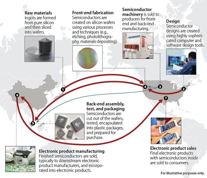
Semiconductors: U.S. Industry, Global Competition, and Federal Policy

                 Figure 5. Typical Global Semiconductor Production Pattern

     Source: CRS, adapted from information provided by SIA.

Materials Used for Wafer Manufacturing
Silicon is still the most widely used basic material on which semiconductors are fabricated. Five
firms account for 90% of the world’s silicon wafer production; two Japanese firms, Shin-Etsu and
Sumco, account for around 60%.34 Silicon wafers are manufactured in a number of countries
around the world, including the United States, Japan, Taiwan, Malaysia, and the United Kingdom.
In addition to silicon-based semiconductors, chips referred to as “III-V” semiconductors are cut
from wafers made from a combination of one or more elements each from groups III and V on the
periodic table, such as gallium arsenide (GaAs), silicon carbide (SiC), and gallium nitride
(GaN).35 These materials are most often used in the manufacture of photovoltaics (e.g., solar
cells), light-emitting diodes (LEDs), sensors, optoelectronics, and other products.
III-V semiconductors are generally characterized by a wide bandgap,36 which offers a variety of
improved performance characteristics over silicon. According to the U.S. Department of Energy
(DOE):

34 Siltronic, Siltroni-A Leading Producer of Silicon Wafer, Factbook, Investor Relations, August 2020, p. 4, at
https://www.siltronic.com/en/investors/reports-and-presentations.html.
35 A more recent numbering system for element groups in the periodic table, recommended by the International Union

of Pure and Applied Chemistry (IUPAC), labels groups III and V as groups 13 and 15, but the term “III-V” is most
widely used for this class of semiconductor materials.
36 The bandgap is the energy difference between the valence band and the conduction band of a solid material. No

electronic state can exist between these bands. Wide bandgap materials permit devices to operate at much higher
voltages, frequencies, and temperatures.

Congressional Research Service                                                                                   10
Semiconductors: U.S. Industry, Global Competition, and Federal Policy
Wide bandgap semiconductor materials allow power electronic components to be smaller,
faster, more reliable, and more efficient than their silicon-based counterparts. These
capabilities make it possible to reduce weight, volume, and life-cycle costs in a wide range
of power applications. Harnessing these capabilities can lead to dramatic energy savings in
industrial processing and consumer appliances, accelerate widespread use of electric
vehicles and fuel cells, and help integrate renewable energy onto the electric grid. 37
Other advantages of III-V semiconductors, which vary among the different types, include
radiation resistance (especially important to the defense, space, and nuclear energy sectors);
operation at higher voltages, frequencies, and temperatures; higher processing speeds; faster
switching speeds with lower transition losses; higher power density; and higher material
strength.38
The DOE Office of Energy Efficiency and Renewable Energy supports research on III-V
semiconductors, and sponsors the PowerAmerica Manufacturing USA institute (see “Current
Federal R&D Efforts” for more information on PowerAmerica).
Design; Fabrication; and Assembly, Testing, and Packaging
Semiconductor manufacturing has three distinct components. Some companies specialize in a
particular component, while others engage in two or three.
1. Design, in which companies conceive new products and specifications to meet
customer needs and reduce these ideas to particular logic and circuit designs for
manufacture;
2. Front-end fabrication, in which fabs are used to manufacture semiconductors
by etching microscopic electronic circuits onto wafers of silicon (or, less
commonly, other materials); and
3. Back-end assembly, testing, and packaging (ATP), in which wafers are sliced
into individual semiconductors, encased in plastic, and put through a quality-
control process.
Front-end fabrication and back-end ATP both require highly specialized machinery. SIA estimates
that 90% of the value of a semiconductor chip is split evenly between the design and fabrication
stages, while the remaining 10% is added during the ATP stage.39
Companies that design semiconductors may or may not have their own foundries to make chips.
An integrated device manufacturer (IDM) conducts chip design, fabrication, and ATP in-house.
IDMs include Intel, Samsung, SK Hynix, Micron, Texas Instruments, Toshiba, Sony,
STMicroelectronics, Infineon, and NXP. Some IDMs also provide contract fabrication services
for other firms. A fabless firm, by contrast, engages solely in chip design and partners with a
37 DOE, Office of Energy Efficiency and Renewable Energy, Advanced Manufacturing Office, “Wide Bandgap
Semiconductors: Pursuing the Promise,” at https://www1.eere.energy.gov/manufacturing/rd/pdfs/
wide_bandgap_semiconductors_factsheet.pdf.
38 DOE, Office of Energy Efficiency and Renewable Energy, Advanced Manufacturing Office, “Wide Bandgap
Semiconductors: Pursuing the Promise”; Applied Materials, “Wide Band Gap—The Revolution in Power
Semiconductors,” at http://www.appliedmaterials.com/nanochip/nanochip-fab-solutions/april-2019/wide-band-gap; and
Texas Instruments, “Advantages of Wide Band Gap Materials in Power Electronics—Part 1,” at https://e2e.ti.com/
blogs_/b/powerhouse/archive/2016/05/24/advantages-of-wide-band-gap-materials-in-power-electronics-part-1.
39 John VerWey, Global Value Chains: Explaining U.S. Bilateral Trade Deficits in Semiconductors, USITC, Executive
Briefing on Trade, March 2018, p. 1, at https://www.usitc.gov/publications/332/executive_briefings/ebot-
semiconductor_gvc_final.pdf.
Congressional Research Service 11Semiconductors: U.S. Industry, Global Competition, and Federal Policy contract foundry (a foundry that typically has limited or no semiconductor design capability) to manufacture a design into chips. “Fab-lite” semiconductor companies, such as Infineon, maintain some in-house fabrication production, but contract a significant amount of chip production to outside foundries. Design According to the research firm Trendforce, seven of the top 10 fabless semiconductor design firms, by revenue, are headquartered in the United States—including the top three (Broadcom, Qualcomm, and Nvidia); three are headquartered in Taiwan.40 In 2020, Nvidia bid to acquire ARM—a United Kingdom-headquartered company acquired by Japan’s SoftBank in September 2016—potentially adding to U.S.-headquartered design capabilities.41 Fabless semiconductor firms generally have higher and less volatile profit margins than semiconductor manufacturers with integrated operations.42 Among the risks faced by fabless firms are quality control and ensuring timely production when demand for outside foundries’ capacity is strong. The number of fabless design companies is increasing as some IDMs choose to become fabless and new companies enter the market.43 For some U.S. policymakers, the reliance of U.S. fabless firms on merchant foundries in East Asia to produce chips has raised national security concerns (such as increased risks of concentration by geography and among a small number of companies, the possibility of intellectual property loss due to the need to share details of chip design and production with foundries, assured access to production capacity, and control of product integrity), especially as it relates to leading-edge, 7nm-and-below chip production. According to a report produced for the U.S. Air Force in 2019, “Close to 90% of all high-volume, leading-edge IC production will soon be based in Taiwan, [China], and South Korea, with the U.S. share of global IC fab capacity falling to 8% by 2022, down from 40% in the 1990s.”44 There is competition in semiconductor design focused on unique functions. These include chip design for personal computers (including memory chips), video and graphic processing and display, servers, tablets, cellphones, automobiles, digital televisions, set-top boxes, game consoles, medical devices, wearable systems, wireless networks, military systems, and other industrial applications. Some of these chips may also incorporate artificial intelligence to varying degrees. Figure 6, produced by market research firm IC Insights in 2017, shows estimated 2017 revenues for selected IC end-use markets, the share of global revenues for each in 2017 (on the y-axis), and the projected compound annual growth rate for revenues from 2016 to 2021 (on the x-axis). ICs for cell phones and personal computers (PCs) were the two largest segments, together accounting for more than 40% of global IC revenues. The two segments with the fastest projected compound 40 TrendForce, “Global Top 10 IC Designers’ 2019 Revenues Drop by 4.1% YoY, as Industry Growth to Face Challenges from Covid-19 Pandemic in 2020, Says TrendForce,” press release, March 17, 2020, at https://press.trendforce.com/node/view/3341.html. 41 Nvidia, Nvidia to Acquire ARM for $40 Billion, Creating World’s Premiere Computing Company for the Age of AI, September 13, 2020, at https://nvidianews.nvidia.com/news/nvidia-to-acquire-arm-for-40-billion-creating-worlds- premier-computing-company-for-the-age-of-ai. 42 Angelo Zino and Jien Loon Choong, Semiconductors and Semiconductor Equipment, CFRA Industry Surveys November 2019, p. 31. 43 Angelo Zino and Jia Yi Young, Semiconductors and Semiconductor Equipment, CFRA, May 2020, p. 25. 44 Rick Switzer, U.S. National Security Implications of Microelectronics Supply Chain Concentrations in Taiwan, South Korea, and the People’s Republic of China, p. 4, September 2019, as prepared for the U.S. Air Force, Office of Commercial and Economic Analysis. Congressional Research Service 12
Semiconductors: U.S. Industry, Global Competition, and Federal Policy

annual growth rate (CAGR) for revenues during the 2016 to 2021 period were automotive (13.4%
CAGR) and IoT (13.2% CAGR). The CAGR for all IC revenues for this period was 7.9%,
growing from $297.7 billion in 2016 to a projected $434.5 billion in 2021.45 Likely areas of
growth beyond 2021 include automotive and IoT. These market shares and growth rates pertain
only to a portion of the entire IC market.

      Figure 6. Integrated Circuit End-Use Markets and Estimated Growth Rates
                                                  Dollars in billions

     Source: IC Insights, Research Bulletin, Automotive and IoT Will Drive IC Growth Through 2021, December 6, 2017,
     provided to CRS by IC Insights in email communication, August 27, 2020.
     Notes: Data for 2017 based on estimated sales. Compound annual growth rates (CAGR) for 2016-2021 based
     on 2016 sales and projected sales for 2021.

Beyond fabless design firms and IDMs, competitors in these markets include companies in other
industries. Facebook designs chips optimized for the types of content it stores and processes on its
servers. Apple develops chips for the iPhone and the iPad. Automakers are working with partners
to develop chips that support electric and hybrid-electric vehicles, as well as to support
autonomous driving functions. In each case, the physical production of the custom-designed chips
is performed by contract foundries.
Semiconductor designers often rely on other companies for IP cores46 and electronic design
automation (EDA) software.47 Designers work with foundries to ensure that their designs can be
reliably manufactured.48 Fabless firms work in close coordination with contract fabs. For
example:

45 IC Insights, Research Bulletin, Automotive and IoT Will Drive IC Growth Through 2021, December 6, 2017,
provided to CRS by IC Insights in email communication, August 27, 2020.
46 An intellectual property (IP) core is a reusable component of design logic with a defined interface and behavior. Arm

Holdings is the largest company that sells and licenses IP cores. Nvidia is in talks to acquire ARM. (George Leopold,
“Nvidia Said to be Close on Arm Deal,” HPC Wire, August 3, 2020, at https://www.hpcwire.com/2020/08/03/nvidia-
said-to-be-close-on-arm-deal/.)
47 EDA firms make the specialized software that is used to design all semiconductor devices. The three largest EDA

companies are Cadence (U.S.), Synopsys (U.S.), and Mentor Graphics (Germany).
48 McKinsey & Company, Semiconductor Design and Manufacturing: Achieving Leading-Edge Capabilities, August

20, 2020, p. 4, at https://www.mckinsey.com/industries/advanced-electronics/our-insights/semiconductor-design-and-
manufacturing-achieving-leading-edge-capabilities.

Congressional Research Service                                                                                        13
You can also read


