Technology Strategy to Drive Moore's Law into Next Decade - Martin van den Brink President and Chief Technology Officer
←
→
Page content transcription
If your browser does not render page correctly, please read the page content below
Technology
Strategy to Drive
Moore’s Law into
Next Decade

Martin van den Brink
President and
Chief Technology Officer

                           Public
Technology strategy                                           • Holistic Lithography roadmap is driven by our unique
    Key messages                                                    patterning control solutions that deliver customer value via                Slide 2
                                                                                                                                          29 Sept. 2021
                                                                    improved on product performance.

• Moore’s Law is alive and well! Industry innovation              • ASML’s comprehensive product portfolio is aligned to our
  continues, fueled by system scaling, delivering highly valued     customers’ roadmaps, delivering cost effective solutions in support
  semiconductor products.                                           of all applications from leading edge to mature nodes

• Semiconductor system scaling enables exponential                • Our next generation EUV technology, High-NA, is progressing
  performance improvement and energy reduction in support of        well and will be the engine to drive the lithography roadmap into
  significant growth of data exchange.                              the next decade

• Customers’ roadmaps require continued shrink and                • Continued execution of our strategic priorities is expected to
  reduction in edge placement error to drive affordable scaling     provide cost effective solutions for our customers, enable the
  into next decade.                                                 extension of the industry roadmap into the next decade, and
                                                                    support our long-term sustainability commitment

                                                                                                                                                  Public
• Moore’s Law evolution
  and customer roadmap

ASML’s strategic priorities

                              Public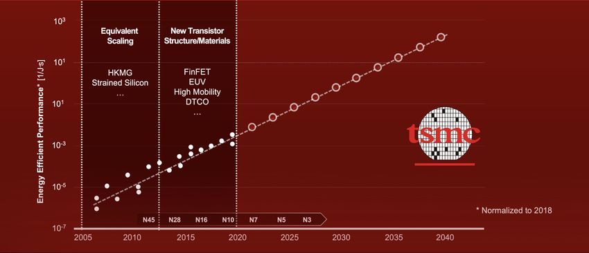
Significant device innovation in logic ahead of us
  scaling roadmap continues to 1 nm and beyond                                                                                                                         Slide 4
                                                                                                                                                                 29 Sept. 2021

             3 nm                                            2 nm                                     1,5 nm                              1 nm and beyond
     PP: 44-48, MP: 21-24                          PP: 40-44, MP: 18-21                       PP: 40-44, MP: 18-21                        PP: 38-42, MP: 15-18

                                                       BPR
                                            BPR
       FinFET                         Nanosheets, BPR               Forksheets, VHV std cell arch. CFET, BEOL w/airgaps                          2D atomic channels
          5T                                      5T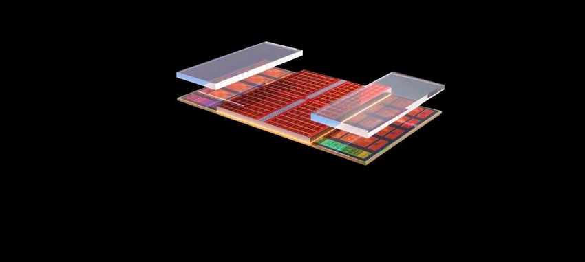
Innovation is not limited to device level
TSMC’s system roadmap to >300 B transistors                                                                                                                                                              Slide 5
                                                                                                                                                                                                   29 Sept. 2021
                                                                            WoW: Wafer on Wafer CoWoS: Chip on Wafer on Substrate   HBM: 3D High Speed Memory   RDL: Re Distribution Layer
                                                      SOC: System on Chip   CoW: Chip on Wafer  FPGA: Field Programmable Grid Array InFo: Integrated Fan-Out    SoIC: System on Integrated Chips

                                                                                                                                                     > transistors
                                                                                                                                                       300 B                             TSMC - SoIC™️

                                                                                              InFo                 150B
                                                                                                                 transistors

                      CoWos

                                                                                                                                                       > 50 B
                                                                                                                  15B                                      transistors
                                                                                                               transistors
                                                                   7B
                                                               transistors
                          200 MOS transistors
    A few transistors

                                                                                                          3D FinFET                                   New channel materials
                                                                 HKMG                                 2P2E                                     EUV
                                                           Immersion                            ELK                                       Metal oxide ESL
                                                    SiGe                                 Low-R Barrier                              Self-aligned line w/ flexible space
                                              Cu/LowK                               Co Capliner                                Low damage/hardening low-k & novel Cu fill

Source: Mark Liu, TSMC, “Unleash the future of innovation” ISSCC, Feb 15, 2021                                                                                                                             Public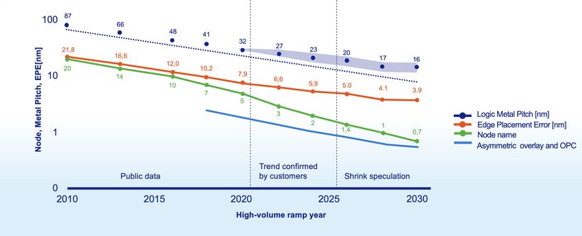
Innovation is not limited to device level
TSMC’s system roadmap to >300 B transistors                                                                                                                                                              Slide 6
                                                                                                                                                                                                   29 Sept. 2021
                                                                            WoW: Wafer on Wafer CoWoS: Chip on Wafer on Substrate   HBM: 3D High Speed Memory   RDL: Re Distribution Layer
                                                      SOC: System on Chip   CoW: Chip on Wafer  FPGA: Field Programmable Grid Array InFo: Integrated Fan-Out    SoIC: System on Integrated Chips

  Device scaling (Including foundry supply chain)
  Circuit scaling (Including foundry customers)
                                                                                                                                                     > transistors
                                                                                                                                                       300 B                             TSMC - SoIC™️

  Dimensional scaling (Including litho supply chain)                                          InFo                 150B
  Architectural scaling by foundry customers                                                                     transistors

                      CoWos
                                                                                                                                                                           Chip level towards
                                                                                                                                                                           system level

                                                                                                                                                       > 50 B
                                                                                                                  15B                                       transistors
                                                                                                               transistors
                                                                   7B
                                                               transistors
                          200 MOS transistors
    A few transistors

                                                                                                           3D FinFET                                 New channel materials
                                                                 HKMG
                                                                                                      2P2E                                     EUV
                                                                                                ELK                                       Metal oxide ESL
                                                           Immersion
                                                    SiGe                                 Low-R Barrier                               Self-aligned line w/ flexible space
                                              Cu/LowK                               Co Capliner                                Low damage/hardening low-k & novel Cu fill

Source: Mark Liu, TSMC, “Unleash the future of innovation” ISSCC, Feb 15, 2021                                                                                                                             Public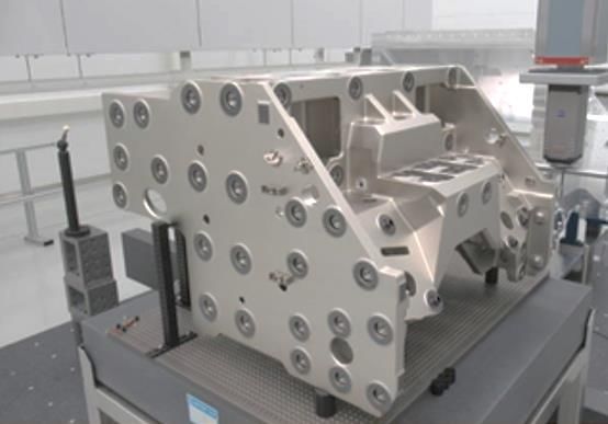
Moore’s Law evolution: the next decade
       Traditional scaling metrics like clock frequency have been saturated since 2005                                                                                        Slide 7
                                                                                                                                                                        29 Sept. 2021

                                                                              Public data           Customer          Speculation
1020                                                                                                projection
                                                           Dennard      Post Dennard
1018                                                        scaling     scaling

1016

1014

1012

1010

108

106

104                                                                                                                                                      Clock Frequency1
                                                                                                                                                         [MHz]
102
 1
      1970             1980              1990               2000              2010              2020              2030

     Source: ¹Karl Rupp as published by: Shekar Bokar, QUALCOMM, “Future of computing in the so-called post Moore’s Law era”, International conference
     for high performance computing, networking storage and analysis, November 18, 2020.                                                                                        Public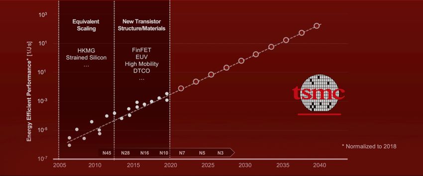
Moore’s Law evolution: the next decade
       Scaling metric of transistor and litho density continues in this decade                                                                               Slide 8
                                                                                                                                                       29 Sept. 2021

                                                                         Public data     Customer       Speculation
1020                                                                                     projection
                                                          Dennard    Post Dennard
1018                                                       scaling   scaling

1016

1014

1012

1010                                                                                                                             Transistor density2
                                                                                                                                 [#/mm2]
108                                                                                                          Device and layout
                                                                                                             optimization        Litho density2
106                                                                                                                              (Contact Poly Pitch*Metal Pitch)-1
                                                                                                                                 [109/mm2]
104                                                                                                                              Clock Frequency1
                                                                                                                                 [MHz]
102
 1
      1970             1980             1990              2000          2010           2020           2030

       Sources: ¹Karl Rupp 2ASML data and projection using Rupp                                                                                                Public
Moore’s Law evolution: the next decade
       A system metric measuring energy and time efficiency combined                                                                                                                                             Slide 9
                                                                                                                                                                                                           29 Sept. 2021

                                                                                             Public data               Customer              Speculation
1020                                                                                                                   projection
                             •      Energy-Efficient Performance   for systems and devices defined as
                                                     Dennard Post Dennard
1018                                                                     scaling      scaling

1016
                                                                                                                                                   [1/J.s]
1014
                             •      If applied per single device:
1012
                                                                            EEP = fc/e
1010                                                                        fc = clock frequency [s-1]                                                                               Transistor density2
                                                                                                                                                                                     [#/mm2]
108                                                                         e = the transistor switch energy [J] Device and layout
                                                                                                                                                 optimization                        Litho density2
106                                                                                                                                                                                  (Contact Poly Pitch*Metal Pitch)-1
                                                                                                                                                                                     [109/mm2]
                             •      Using the Dennard¹ scaling model, when the dimension scales with                                                                        k-1,     frequency with k,
104                                                                                                                                                                                  Clock Frequency1
                                    area with k-² and power density constant, it follows:                                                                                            [MHz]
102
                                                •      EEP on-device level scales with k4
 1
      1970
                             •
                           1980
                                    If density
                                           1990
                                               (~k2) scales
                                                       2000
                                                            2x every
                                                                 2010
                                                                     2 year, then
                                                                             2020
                                                                                  EEP (~k 4) scales 4x every 2 year
                                                                                       2030

       1Source: Robert H. Dennard et al. “Design of ion implanted MOSFET’s with very small physical dimensions”, IEEE Journal of solid-state circuits, vol SC 9, October 1973, pp.   256-268.                      Public
Moore’s law evolution: the next decade
       Device Energy Efficient Performance growth been saturated since 2005                                                                                   Slide 10
                                                                                                                                                         29 Sept. 2021

                                                                          Public data     Customer       Speculation
1020                                                                                      projection
                                                           Dennard    Post Dennard                                                 System Energy
                                                            scaling   scaling                                                      Efficient Performance3
1018
                                                                                                                                   [1/J.s]
1016                                                                                                          From transistor to
                                                                                                              system scaling

1014                                                                                                                               Transistor Energy
                                                                                                                                   Efficient Performance2
1012                                                                                                                               [[1/J.s]

1010                                                                                                                               Transistor density2
                                                                                                                                   [#/mm2]
108                                                                                                           Device and layout
                                                                                                              optimization         Litho density2
106                                                                                                                                (Contact Poly Pitch*Metal Pitch)-1
                                                                                                                                   [109/mm2]
104                                                                                                                                Clock Frequency1
                                                                                                                                   [MHz]
102
 1
      1970             1980              1990              2000          2010           2020           2030             2040

       Sources: ¹Karl Rupp, 2 ASML data and projection using Rupp                                                                                                Public
Moore’s Law evolution: the next decade
System Energy Efficient Performance growth 3x/2yrs continues to 2040 Slide 11
29 Sept. 2021
Public data Customer Speculation
1020 projection
System improvements System
1018 dominated by Transistor scaling scaling
1016
1014 Transistor Energy
Efficient Performance2
1012 [1/J.s]
1010 Transistor density2
[#/mm2]
108 Device and layout
optimization Litho density2
106 (Contact Poly Pitch*Metal Pitch)-1
[109/mm2]
104 Clock Frequency1
[MHz]
102
1
1970 1980 1990 2000 2010 2020 2030
Source: TSMC, Mark Liu, “Unleash the future of innovation” ISSCC, Feb 15, 2021. PublicMoore’s law evolution: the next decade
From cost per transistor through density, to cost of time and energy through systems Slide 12
29 Sept. 2021
Public data Customer Speculation
1020 projection
Dennard Post Dennard System Energy
scaling scaling Efficient Performance3
1018
[1/J.s]
1016 From transistor to
system scaling
1014 Transistor Energy
Efficient Performance2
1012 [[1/J.s]
1010 Transistor density2
[#/mm2]
108 Device and layout
optimization Litho density2
106 (Contact Poly Pitch*Metal Pitch)-1
[109/mm2]
104 Clock Frequency1
[MHz]
102
1
1970 1980 1990 2000 2010 2020 2030 2040
Sources: ¹Karl Rupp, 2ASML data and projection using Rupp, 3Mark Liu, TSMC, normalized to transistor EEP in 2005. PublicMoore’s law evolution: the next decade
System scaling to satisfy the need for performance and energy consumption Slide 13
29 Sept. 2021
1020
System improvements System Energy
System Efficient Performance3
1018 dominated by Transistor scaling scaling [1/J.s]
1016 From transistor to
system scaling
1014 Transistor Energy
Efficient Performance2
1012 [[1/J.s]
1010 Transistor density2
[#/mm2]
108 Device and layout
optimization Litho density2
106 (Contact Poly Pitch*Metal Pitch)-1
[109/mm2]
104 Clock Frequency1
[MHz]
102
1
1970 1980 1990 2000 2010 2020 2030 2040
Sources: ¹Karl Rupp, 2ASML data and projection using Rupp, 3Mark Liu, TSMC, normalized to transistor EEP in 2005. PublicAMD 3D chiplet gives an 3.1-3.8 EEP improvement
By integrating memory with the processor in one package Slide 14
29 Sept. 2021
3x power reduction,
Structural silicon
4-25% speed improvement
64MB L3 cache die
Direct copper-to-copper bond
Through Silicon Vias (TSVs) for
silicon-to-silicon communication
Up to 8-core “Zen 3” CCD
Source: Lisa Su, AMD,
“Accelerating the ecosystem”, Computex keynote 2021, June 2 2021
PublicMoore’s law evolution: the next decade
System scaling to satisfy the need for performance and energy consumption Slide 15
29 Sept. 2021
Public data Customer Speculation
1020 projection
System improvements System Energy
System Efficient Performance3
1018 dominated by Transistor scaling scaling [1/J.s]
1016 From transistor to
system scaling
1014 Transistor Energy
Efficient Performance2
1012 [[1/J.s]
1010 Transistor density2
[#/mm2]
108 Device and layout
optimization Litho density2
106 (Contact Poly Pitch*Metal Pitch)-1
[109/mm2]
104 Clock Frequency1
[MHz]
102
1
1970 1980 1990 2000 2010 2020 2030 2040
Sources: ¹Karl Rupp, 2ASML data and projection using Rupp, 3Mark Liu, TSMC, normalized to transistor EEP in 2005. PublicLitho density scaling continues in this decade
Overlay and Optical Proximity Correction errors shrink aggressively Slide 16
29 Sept. 2021
2x every 6 years
Source: Average customer roadmap extended by ASML extrapolation May 2021, averaged with 2020 IRDS Roadmap Mustafa Badaroglu,
“IRDS IFT – More Moore Spring meeting, IEEE, April 21, 2020 PublicMemory roadmap for the next decade
DRAM scaling below 10 nm and NAND stacking continues > 600 layers Slide 17
29 Sept. 2021
DRAM
After 10 years Now Challenge < 10 nm
1y 1z 1a 1b 1c 1d 0a
NAND
After 10 years Now Challenge > 600 layers
96 128 176 2xx 3xx 4xx 5xx 6xx
Source: Sk hynix, S.H.Lee, "Memory's journey towards the future ITC world, IEEE IRPS 21 March 21, 2021 PublicProjection of lithography layers by technology
Slide 18
29 Sept. 2021
KrF
Logic Layer stack
5 nm 3 nm 2 nm ~1.5 nm 1 nm
DRAM
KrF
EUV – High-NA
Layer stack
EUV
1A 1B 1C 0A 0B
ArFi
ArF
KrF
KrF I-Line
3D-NAND Layer stack
176L 2xxL 3xxL 4xxL 5xxL
2021 ~2030
Source: ASML Corporate Strategy and Marketing estimates PublicProjection of lithography layers by technology
Lithography layer count grows, driven by DUV and EUV Slide 19
29 Sept. 2021
KrF
Logic Layer stack
5 nm 3 nm 2 nm ~1.5 nm 1 nm
DRAM
KrF
EUV – High-NA
Layer stack
EUV
1A 1B 1C 0A 0B
DUV
KrF
3D-NAND Layer stack
176L 2xxL 3xxL 4xxL 5xxL
2021 ~2030
Source: ASML Corporate Strategy and Marketing estimates PublicSemiconductor and shrink roadmap: the next decades
Slide 20
29 Sept. 2021
10⁵
In the next decade, system scaling continues to fuel the need
of advanced semiconductor solutions where litho shrink
Relative manufacturing cost per component
1962
10⁴
remains key to improving circuit density and cost.
1965
10³
10² 1970
Implications for ASML
10
The shrink roadmap requires innovation to improve litho
1
performance at lower cost and higher productivity.
1 10 10² 10³ 10⁴ 10⁵
Number of components per integrated circuit
We continue to safeguard our approach by developing trusting
relationships with customers, with stronger holistic products.
PublicMoore’s Law evolution
and customer roadmap
• ASML’s strategic priorities
PublicASML’s strategic priorities
Slide 22
29 Sept. 2021
Strengthen ▪ Enhance execution capabilities to deliver performance, cost
customer trust and robustness to customers needs
Holistic litho and
applications
▪ Build a leading position in edge placement error
DUV
competitiveness ▪ Drive DUV performance and market share
EUV
industrialization ▪ EUV high-volume production performance, ramp and support
High-NA ▪ Enable litho simplification for future nodes
PublicOur holistic portfolio is more important than ever
Slide 23
Lithography scanner with 29 Sept. 2021
advanced control capability
EUV: NXE platform DUV: XT and NXT Etch and
platform deposition tools
Process window Process window
Prediction and Control
Enhancement
Optical proximity correction YieldStar E-beam
Computational lithography Optical metrology
and computational metrology E-beam metrology
E-beam inspection
Process window
Detection PublicOur holistic portfolio is more important than ever
Slide 24
29 Sept. 2021
EUV DUV
High-NA
Applications
PublicAPPS Applications: strategic directions
Deliver leading solutions for optical and e-beam metrology and inspection Slide 25
29 Sept. 2021
Customer Value ASML Apps product roadmap
Capturing more wafer signatures to • Productivity
improve robust on-wafer process control • Robust alignment schemes
Nanometers
Tighter process capabilities • Single Beam resolution and applications
3→6 sigma control • Edge Placement Error control
• Free-Form OPC and Machine Learning
Good wafers Capturing small defects for • Multibeam resolution
per day per yield of advanced nodes • Computationally guided inspection
unit cost
More measurements at fixed • Productivity/multibeam
metrology & inspection budget • E-beam platform consolidation
• OPC accuracy, speed and user-friendliness
Faster time-to-solution • Single process control platform and analytics
Time to yield
PublicAPPS E-beam inspection has inherent resolution advantage
Increasing throughput through increasing parallelism with multibeam Slide 26
29 Sept. 2021
1000000 Min defect size for
2 nm node and below
100000 Optical
Bright Field
Inspection
10000
1000 Gen 3 Multibeam (~2028)
Throughput [mm²/hr]
Increased
100
throughput
enables
10 additional HVM Gen 2 Multibeam (~2024)
applications
1
0.1 Gen 1 Multibeam (2021)
0.01 Scanning
electron
microscope
0.001 image Single e-beam (R&D)
0.0001
60 40 20 10 8 6 4 2 1
Defect size [nm] PublicAPPS Metrology, Inspection & Patterning Control Roadmap
Slide 27
29 Sept. 2021
Platform Application 2020 2021 2022 2023 2024 ≥ 2025
Process Control (Litho InSight) Overlay / Focus CD Optimization Edge Placement Optimization
Scanner Interfaces
Scanner Matching & Stability (Baseliner) Baseliner MMO Baseliner 3 Next Generation
Increasing Scanner Actuation (DUV and EUV), EPE Control
and Control
Control Software(Overlay Optimizer) V3: XY correction per exposure V4: XY correction per exposure, higher order through slit V5: Next Gen
Interface
(Imaging Optimizer) V2: Z correction per exposure V3: Die based Focus and Leveling optimization V4: Next Gen
Overlay Metrology
Alignment 4 colors recipe Fast Stages, Multiple
12 colors recipe Wavelengths, Computational Metrology, 12 color next
YieldStar In-Device Metrology
Overlay / Focus (After litho) YS380 YS385 Increased speed, accuracy YS500 Increased speed, accuracy YS Next Generation
(Optical)
In device Overlay (After etch) YS1375 Device Overlay YS1385 Increased Speed YS1390 Increased Speed YS Next Generation
Metrology
E-beam
CD / EPE Metrology eP5 0.1nm precision, 12umSingle
field of view, Beam High
Resolution, Large
9KeV HLE (option)eP6Field of View,
Higher Precision, Higher Resolution eP7 Next Generation
(E-Beam) Metrology
3D Metro + Inspection Massive Metrology, EPE metrology
eP5XS 18.5KeV landing energy eP5XLE 30KeV landing energy eP7XLE
50KeV landing energy
Precision Inspection: eScan600 high resolution with 2nm pixel size eScan700
(Single beam) Higher Throughput
E-Beam Defect eScan430 large current with throughput enhancement eScan460 Higher throughput, higher resolution, transient inspection
VC and physical, landing
energy >30KeV
Multi-beam, Fast and Accurate Stages, High Landing Energy, Guided Inspection
Inspection Inspection eScan1000 9 beams (3x3) eScan1100 (5x5) 25 beams eScan1200 (5x5) higher throughput, large current
(E-Beam) High Productivity Inspection:
(Multi beam) eScan2200
higher resolution, higher throughput
Computational
Guided Inspection Die to database Improved Model Accuracy, Inverse OPC, Guided Inspection e-beam inspection throughput enhancement
Computational
fast defect detection, higher sensitivity
Lithography Machine and Deep Learning, Etch Models
OPC Model Accuracy 1.5nm 1.3nm 1.0nmDUV NXT:2050i in volume manufacturing at customers
20% overlay improvement, faster reliability and productivity ramp-up Slide 28
29 Sept. 2021
NXT:2050i
Matched machine Dedicated chuck
overlay ~1.2 nm overlay ~0.8 nm
6000 5,000 wafers per day in 18 days 200 180 hours reliability in 13 weeks
180
5000
NXT:2050i 160 NXT:2050i
Faster ramp 140 Higher availability
Wafers per day
MTBI (hours)
4000
120
3000 100
80
2000
60
40
1000
20
0 0
1 2 3 4 5 6 7 8 9 10 11 12 13 14 15 16 17 18 19 20 21 22 23 1 2 3 4 5 6 7 8 9 10 11 12 13 14 15 16 17 18 19
Days after completing installation
NXT:2000i Weeks after completing installation
NXT:2050i PublicDUV DUV: Strategic directions
Deliver leading solutions for advanced capabilities and higher productivity Slide 29
29 Sept. 2021
Customer value ASML DUV product roadmap
Overlay Improve overlay (stability) especially • NXT:2100i with optics and alignment improvements
for matching to EUV
More good wafers per day at • Immersion productivity increase through
Productivity &
lower cost per wafer higher scan speed
Availability • XT to NXT transition for dry lithography
Installed base Cost-competitive service offerings for • Productivity Enhancement Packages for installed base
entire product lifecycle • Value added service solutions increasing availability at
node performance
New markets Productivity and overlay performance for • Mature XT platform with application specific options
specific applications • Extend i-line product portfolio for Mature markets (>40nm)
• Fab replacement solutions
Circular Sustainable product & service offerings • System Node Extension Package roadmap
economy • Optimize re-use to secure cost competitive supply
PublicDUV DUV product portfolio to support all market segments
Slide 30
29 Sept. 2021
Wavelength NA, Half pitch 2020 2021 2022 2023 2024 2025
NXT:2000i NXT:2050i NXT:2100i NEXT
Continue
critical innovation on advanced NXT platform for improved imaging, overlay and productivity
2.0 nm | 275wph 1.5 nm | 295wph 1.3 nm | 295wph
ArFi 1.35 NA, 38 nm
NXT:1980Di NXT:1980Ei NXT:1980Fi
Leverage
mid - critical of advanced NXT platform for improved productivity
2.5 nm | 275wph 2.5 nm | 295wph 2.5 nm | 330wph
XT
XT:1460K
5 nm | 205wph or 7.5 nm| 228wph
ArF 0.93 NA, 57 nm to advanced NXT platform for improved imaging, overlay and productivity
Migrate
NXT:1470 NEXT
NXT
4 nm | 300wph
0.93 NA, 80 nm XT:1060K XT:1060K + PEP
Productivity increases on XT platform
5 nm | 205wph 5 nm | 220wph
XT:860M XT:860N
KrF Productivity
XT
7increases
nm** | 240 on
- 250wph
XT platform 7.5 nm | 260wph
0.80 NA,110 nm
Migrate to advanced NXT platform for performanceNXT:870
and productivity NEXT
NXT
7.5 nm | 330wph
XT:400L XT:400M NEXT
i-line 0.65 NA, 220 nm
Productivity increases on XT platform and migrate to next system for high volume applications
20 nm** | 230wph 20 nm** | 250wph
27% 34% 30%
Product: Matched Machine Overlay* (nm)|Throughput(wph)
5%
95% 66% 70%
Product status Released Development Definition **Wafer inner field PublicEUV EUV 0.33 NA adoption enabled by platform maturity in
high-volume manufacturing Slide 31
29 Sept. 2021
100%
3000
System output
Max wafers per day (single system, weekly average) 95%
2500 90%
Installed base system availability
Wafers per day
Availability
4 weeks moving average (end of period) 85%
2000
80%
75%
1500
70%
1000 65%
60%
500
55%
50%
0
2017 2018 2019 2020 2021
ASML commitment is expected to bring EUV availability >95%
and increase wafer per day output >50% by 2025
Source : ASML installed base data PublicEUV EUV: strategic directions
Enabling cost-efficient scaling for advanced nodes Slide 32
29 Sept. 2021
Customer value using EUV ASML EUV product improvements
Better device performance: simpler • Technology roadmap: per node (resolution), improve
design and superior electrical imaging, overlay and defectivity (reticle and wafer
Nanometers performance level)
Less tools needed to meet fab capacity
• Productivity roadmap over time: increase Productivity
due to higher throughput
Productivity to >200wph, Availability to >97%
Patterning cost saving for critical layers vs
alternatives (3x ArFi immersion and
Improvement sub system focus:
above)
Good wafers • Source (in-line refill, higher power, high reflective mirror)
per day per cost Higher yield due to less multiple
• Mirrors (mirror heating measure, cooled mirrors)
patterning layers (up to 9%)
• Stages and reticle (Reticle heating, high-accurate fast
stages, pellicle durability)
Reduced process complexity leading to • Alignment (# marks, mark size, wafer clamp robustness)
Cycle time and shorter learning cycles and faster time-to-
yield
time to market
PublicEUV High-NA to prevent cycle time and process complexity increase
like low NA did for immersion Slide 33
29 Sept. 2021
0.55-NA EUV preferred
0.33-NA EUV Insertion
5
mask steps, cycletime (product dependent)
3
process complexity (a.u.)
DUV EUV- 0.33NA EUV- 0.55NA
3
0.33-NA insertion supports single High-NA insertion opportunities to
patterning to reduce cycle time continue Moore’s Law without any
penalty of cycle time increase
2
Alternative Alternative
Proposed baseline Proposed baseline
1
10 100 1,000
16nm 10nm 7nm 5nm 3nm 2nm
Transistor density [MTr/mm²] Nodes (equivelant node names) [nm]
Note: Assuming 1.2 days per mask layer PublicEUV High-NA EUV: strategic directions
Enabling cost-efficient scaling for next generation advanced nodes Slide 34
29 Sept. 2021
Customer value High-NA EUV ASML High-NA EUV product improvements
0.55 NA enables 1.7x smaller features
and 2.9x increased density • Technology roadmap: per node (resolution), improve
Nanometers imaging, overlay and defectivity (reticle and wafer
level)
Higher imaging contrast enables 40%
improvement in local CDU • Productivity roadmap over time: increase Productivity
Performance 1.4x reduced pattern variability at 1.4x
lower dose
15% Patterning cost saving for critical
Focus for a successful insertion at
layers vs alternatives (2x EUV) our customers
Good wafers • Commonality with existing EUV platform to reduce
per day per cost Higher yield due to less multiple
technological risk, cost of development and switch cost
patterning layers: 35% less mask count
at customer
below 2 nm process node
• Focus on system maturity and serviceability to support
Reduced process complexity leading to our customer high volume performance expectation
15% shorter learning cycles and faster • Early engagement with our customers to address
Cycle time and ecosystems readiness
time-to-yield
time to market
PublicEUV High-NA EUV is in the realization phase
On multiple ASML and supplier locations Slide 35
29 Sept. 2021
Oberkochen, Germany optics system manufacturing facilities
Veldhoven,
the Netherlands,
system bottom test
EUV 0.55 NA optics
Toulon, France, Frame milling Wilton, USA, system top test
PublicEUV EUV 0.55 NA is expected to be added to EUV portfolio
for high volume in 2025 - 2026 while continue improving the 0.33 NA platform Slide 36
29 Sept. 2021
Wavelength NA, Half pitch 2020 2021 2022 2023 2024 ≥2025
NXE:3400C NXE:3600D
0.33NA continuous imaging, NXE:3800E in line
overlay and productivity improvements NXE:4000F
0.33 NA, 13 nm 1.5 nm | 135 wph / 145 wph 1.1 nm | 160 wph 195 wph / 220wph 220 wph
with customers advanced node HVM requirements.
Early Access Customer Customer
EUV Customer timing 0.55 NA ASML R&D HVM
0.55NA enabling affordable scaling beyond current decade
EXE:5000 EXE:5000 EXE:5200
0.55 NA, 8 nm at ASML fabTRUST Commonality across EUV, DUV & High-NA platforms
Allows faster and more cost-effective innovation, production and maintenance Slide 37
29 Sept. 2021
DUV EUV
Alignment Sensor
Level sensor
Common Technology
Metrology
used in both
Wafer handling
DUV & EUV platform
NXT (248nm dry) NXT (193 nm dry) NXT (193 nm wet)
Common Technology
used in
DUV products: NXT
NXT:870 NXT:1470 NXT:2050i
EUV EUV High-NA
Alignment Sensor Source
Level sensor Metrology
Common Technology Wafer stager
used in both Reticle stager
Wafer handling
EUV platforms
PublicTRUST Maximizing customers’ good wafers per day
Next to minimizing system down time Slide 38
29 Sept. 2021
100% 100% 100%
System downtime System downtime serving
according to customer needs
standardized Process-specific inefficiencies
definition >97% e.g., system down to meet
customer specs, layer
qualification after system down,
defectivity monitoring and more > 90-95%
> 85-90%
System uptime System uptime producing
capable of producing customer wafers
wafers
Historical service model: Uptime measuringNew service model:
Maximize scanner availability only good wafers per daygood wafers per day
Maximize
PublicTRUST EUV is the most energy efficient solution
We expect net energy savings of more than 45% over alternative processes Slide 39
29 Sept. 2021
EUV 0.55
EUV 0.33
Electrical power reduction Electrical power reduction
Immersion to EUV 0.33 productivity [wph] EUV 0.33 to EUV 0.55 at 220 wph
Side wall Assisted DryEtch
Quadrupole Patterning
ArFi
EUV Lito-Etch-Litho-Etch 0.33 NA
100 wph Metallization
- 46%
- 45%
Metrology Litho-Etch 0.55 NA
145 wph Deposition
(today) 0 5 10 15 20
WetEtch
220 wph
(2025)
0 5 10 15 20
Source: Sri Samavedam a.o., IMEC, “Future of logic scaling: Towards atomic channels and deconstructed chips”, IEDM, Dec 2020, extended by ASML. PublicTechnology strategy • Holistic Lithography roadmap is driven by our unique
Key messages patterning control solutions that deliver customer value via Slide 40
29 Sept. 2021
improved on product performance.
• Moore’s Law is alive and well! Industry innovation • ASML’s comprehensive product portfolio is aligned to our
continues, fueled by system scaling, delivering highly valued customers’ roadmaps, delivering cost effective solutions in support
semiconductor products. of all applications from leading edge to mature nodes
• Semiconductor system scaling enables exponential • Our next generation EUV technology, High-NA, is progressing
performance improvement and energy reduction in support of well and will be the engine to drive the lithography roadmap into
significant growth of data exchange. the next decade
• Customers’ roadmaps require continued shrink and • Continued execution of our strategic priorities is expected to
reduction in edge placement error to drive affordable scaling provide cost effective solutions for our customers, enable the
into next decade. extension of the industry roadmap into the next decade, and
support our long-term sustainability commitment
PublicForward Looking Statements
Slide 41
29 Sept. 2021
This presentation contains statements that are forward-looking, including statements with respect to expected industry and business environment trends including
expected growth, outlook and expected financial results, including expected net sales, gross margin, R&D costs, SG&A costs and effective tax rate, annual revenue
opportunity for 2025, financial model for 2025 and assumptions and expected growth rates and drivers, expected growth including growth rates 2020-2025 and 2020-
2030, total addressable market, growth opportunities beyond 2025 and expected annual growth rate in lithography and metrology and inspection systems and expected
annual growth rate in installed base management, expected trends in addressable market up to 2030, expected trends in Logic and Memory revenue opportunities, long
term growth opportunities and outlook, expected trends in demand and demand drivers, expected benefits and performance of systems and applications, semiconductor
end market trends, expected growth in the semiconductor industry including expected demand growth and capital spend in coming years, expected wafer demand
growth and investments in wafer capacity, expected lithography market demand and growth and spend, growth opportunities and drivers, expected trends in EUV and
DUV demand, sales, outlook, roadmaps, opportunities and capacity growth and expected EUV adoption, profitability, availability, productivity and output and estimated
wafer demand and improvement in value, expected trends in the applications business, expected trends in installed base management including expected revenues
and target margins, expected trends and growth opportunity in the applications business, expectations with respect to high-NA, the expectation of increased output
capacity, plans, strategies and strategic priorities and direction, expectation to increase capacity, output and production to meet demand, the expectation that Moore's
law will continue and Moore's law evolution, product, technology and customer roadmaps, and statements and intentions with respect to capital allocation policy,
dividends and share buybacks, including the intention to continue to return significant amounts of cash to shareholders through a combination of share buybacks and
growing annualized dividends and statements with respect to ESG commitment, sustainability strategy, targets, initiatives and milestones. You can generally identify
these statements by the use of words like "may", "will", "could", "should", "project", "believe", "anticipate", "expect", "plan", "estimate", "forecast", "potential", "intend",
"continue", "target", "future", "progress", "goal" and variations of these words or comparable words. These statements are not historical facts, but rather are based on
current expectations, estimates, assumptions and projections about our business and our future financial results and readers should not place undue reliance on them.
Forward-looking statements do not guarantee future performance and involve a number of substantial known and unknown risks and uncertainties. These risks and
uncertainties include, without limitation, economic conditions; product demand and semiconductor equipment industry capacity, worldwide demand and manufacturing
capacity utilization for semiconductors, semiconductor end-market trends, the impact of general economic conditions on consumer confidence and demand for our
customers’ products, performance of our systems, the impact of the COVID-19 outbreak and measures taken to contain it on the global economy and financial markets,
as well as on ASML and its customers and suppliers, and other factors that may impact ASML’s sales and gross margin, including customer demand and ASML’s ability
to obtain supplies for its products, the success of R&D programs and technology advances and the pace of new product development and customer acceptance of and
demand for new products, production capacity and our ability to increase capacity to meet demand, the number and timing of systems ordered, shipped and recognized
in revenue, and the risk of order cancellation or push out, production capacity for our systems including the risk of delays in system production and supply chain
capacity, constraints, shortages and disruptions, trends in the semi-conductor industry, our ability to enforce patents and protect intellectual property rights and the
outcome of intellectual property disputes and litigation, availability of raw materials, critical manufacturing equipment and qualified employees and trends in labor
markets, geopolitical factors, trade environment; import/export and national security regulations and orders and their impact on us, ability to meet sustainability targets,
changes in exchange and tax rates, available liquidity and liquidity requirements, our ability to refinance our indebtedness, available cash and distributable reserves for,
and other factors impacting, dividend payments and share repurchases, results of the share repurchase programs and other risks indicated in the risk factors included in
ASML’s Annual Report on Form 20-F for the year ended December 31, 2020 and other filings with and submissions to the US Securities and Exchange Commission.
These forward-looking statements are made only as of the date of this document. We undertake no obligation to update any forward-looking statements after the date of
this report or to conform such statements to actual results or revised expectations, except as required by law.
PublicPublic
You can also read