Towards 1.6T datacentre interconnect technologies: the TWILIGHT perspective - IOPscience
←
→
Page content transcription
If your browser does not render page correctly, please read the page content below
PERSPECTIVE • OPEN ACCESS

Towards 1.6T datacentre interconnect technologies: the TWILIGHT
perspective
To cite this article: Maria Spyropoulou et al 2020 J. Phys. Photonics 2 041002

View the article online for updates and enhancements.

                               This content was downloaded from IP address 46.4.80.155 on 22/11/2020 at 19:59
J. Phys. Photonics 2 (2020) 041002 https://doi.org/10.1088/2515-7647/ab9bf6
Journal of Physics: Photonics
PERSPECTIVE
Towards 1.6T datacentre interconnect technologies: the TWILIGHT
OPEN ACCESS
perspective
RECEIVED
31 January 2020 Maria Spyropoulou1, Giannis Kanakis1, Yuqing Jiao2, Ripalta Stabile2, Nicola Calabretta2,
ACCEPTED FOR PUBLICATION Kevin Williams2, Jean-Yves Dupuy3, Agnieszka Konczykowska3, Richard Schatz4, Oskars Ozolins4,5,
11 June 2020
Jakub Zvěřina6, Martin Žoldák6, Paraskevas Bakopoulos7, Giannis Patronas7 and Hercules Avramopoulos1
PUBLISHED
1
23 July 2020 Photonics Research Communications Laboratory, School of Electrical and Computer Engineering, National Technical University of
Athens, Athens, Greece
2
Original content from
Institute of Photonic Integration, Technical University of Eindhoven, Eindhoven, The Netherlands
3
this work may be used III-V Lab, Palaiseau Cedex, France
4
under the terms of the School of SCI, KTH Royal Institute of Technology, Kista, Sweden
Creative Commons 5
RISE Research Institutes of Sweden AB, Kista, Sweden
Attribution 4.0 licence. 6
Argotech A.S., Trutnov, Czech Republic
7
Any further distribution Mellanox Technologies Ltd., Yokneam, Israel
of this work must
maintain attribution to E-mail: mspy@mail.ntua.gr
the author(s) and the title
of the work, journal Keywords: photonic integration, optical transceivers, optical space switches, wafer-scale bonding, co-packaged optics
citation and DOI.
Abstract
The transformation of datacentres to support the increasing traffic growth requires the
development of new technologies to migrate to 1.6T optical transceivers and to ultra-fast high
radix optical space switches. In this work, an outline of the technological perspectives of
TWILIGHT project is provided in accordance with research updates and industry standards.
1. Introduction
Rapidly growing cloud applications, big data, Internet-of-Things, artificial intelligence and machine learning
are the main drivers for the explosion of datacentre traffic which is foreseen to reach 19.5 ZB per year by 2021
[1]. The increasing traffic demands impose a huge problem for datacentre operators because on one hand
they have to keep pace with the increasing speeds and on the other, they have to cope with the increasing
power consumption that is required for airflow management and cooling [2]. The deployment of hyperscale
datacentres is currently driving the market of 400GbE pluggables, while the next standards ratification for
800 GbE and 1.6 T are expected within the 2023–2024 timeframe [3, 4]. In addition, as datacentres grow in
size, the number of interconnections in multi-tier leaf-spine topologies grow as well, dictating the
deployment of high-radix switches complying with the very stringent latency constraints.
The ratification of 400GbE industry standard in December 2017 [5] has led to multiple 400Gb s−1
demonstrations in 2018 and the availability of the first commercial products in 2019 [6, 7]. 400GbE defines
non-return-to-zero and 16 parallel lanes on multi-mode fibre for short reach 100 m applications, but 4-level
pulse-amplitude-modulation (PAM4) is the dominant format of choice for 500 m, 2 and 10 km. More
specifically, for short reach (i.e. 500 m) applications the use of 4 optical wavelengths based on 100 G PAM4
signalling (i.e. 53.125 Gbaud electrical lane interfaces) is defined, and for 2 and 10 km distances 50 G PAM4
signalling (i.e. 26.5625 Gbaud) is used in combination with 8 optical wavelengths. PAM4 is also considered
for short datacentre interconnect links combined with enhanced DSP chipsets [8].
QSFP-DD and OSFP form factors for 400GbE pluggable modules enable the deployment of next
generation 12.8 T switches upgrading the overall front panel capacity from 3.2 T using current 100GbE
modules by increasing the lane rate from 25 Gb s−1 to 50Gb s−1 . A further increase of the overall switch
capacity falls under the well known switch front panel density bottleneck [9], which dictates on one hand a
further increase of the overall rate per lane to 100Gb s−1 and on the other, the sought of new integration and
packaging schemes for the opto-electronic engines (OE). One approach to overcome the mechanical
dimension limit for additional pluggable connectors in 1RU switch front panel is the use of mid-board
optical transceivers based on COBO standard form factor which allows moving the optics away from the
© 2020 The Author(s). Published by IOP Publishing LtdJ. Phys. Photonics 2 (2020) 041002 M Spyropoulou et al
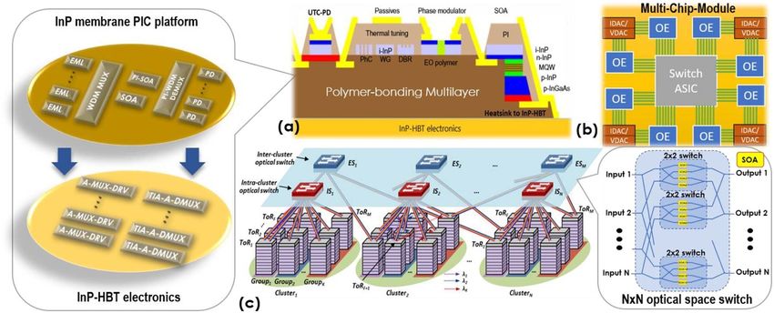
Figure 1. TWILIGHT concept towards next generation datacentres: (a) wafer-scale co-integration of high-speed PICs and
electronics ICs, (b) Co-packaged optoelectronic engines (OE) with switch ASIC scaling to 1.6 T capacity, (c) flat optical
intra-datacentre architecture relying on nanosecond-scale SOA-based NxN optical space switches [16].
faceplate and permits new and creative designs to support the higher thermal requirement of faster and
larger radix digital switches. However, COBO modules are again based on wavelength multiplexing of 8 lanes
limiting the maximum attained overall capacity. What is more, the single-chip switch application specific
integrated circuit (ASIC) capacity has doubled every two years through a combination of increasing channel
count and rate, while optical modules capacity increase is based on a much more gradual incline [10]. 112 G
SERDES products based on 7 nm technology node are already available from the third quarter of 2018 [11,
12] targeting the 112 G-VSR-PAM4 IEEE electrical interface standard which is underway by the IEEE P802.3
100 Gb s−1 Electrical Lane Study Group [13]. Component vendors have announced availability of their
56 Gbaud PAM4 chipsets and 56 G optical components in 2018 and many demonstrations of 100Gb s−1 per
wavelength have been performed [14], which is a clear evidence of the need to move towards higher lane
rates.
Datacentre architectrues have evolved from fat-tree to leaf-spine topologies. Two-layer leaf-spine are the
most commonly deployed architectures for small and medium datacentres (interconnecting tens to hundreds
of top-of-rack (TOR) switches, each interconnecting > 40 servers), while three-layer leaf-spine topologies are
mostly employed for large and mega datacentre environments. Therefore, building a datacentre network
with a large number of servers (>100 000) each operating at high data rate (>100 Gb s−1 ), requires electrical
switches with extremely high radix to avoid hierarchical multi-layer architectures and the resulting
bandwidth bottlenecks, high server-to-server latency as well as poor cost-efficiency [15]. However, the
limited I/O bandwidth of the ASIC caused by the limited ball grid array density will prevent the
implementation of high radix switch at high data rates [9].
In this communication, we report on the optoelectronic technologies, photonics and electronics
co-integration and co-packaging schemes which are necessary to support the increasing traffic and
connectivity requirements within and between datacentres, as these are envisioned under the European
H2020 project TWILIGHT.
2. TWILIGHT concept and approach
Figure 1 illustrates the TWILIGHT concept towards the realization of next generation datacenter
interconnects which relies on wafer-scale bonding of high performance InP system-on-chip membrane
photonics and high speed InP-HBT electronics for the development of 112 Gbaud transceivers and fast
high-radix optical space switches.
2.1. Scaling transceiver capacity to 112 Gbaud per lane
Directly Modulated Lasers (DMLs) and Electro-absorption Modulated Lasers (EMLs) are the dominant
photonic technology for datacentre interconnects [17], with the former to be mostly suitable for short
intra-datacentre links up to 500 m due to their inherent chirp limitations and the latter to be mostly
preferred for 2, 10 km and longer distances. Commercially available 56G EMLs are exhiting 3-dB bandwidth
more than 30 GHz targeting the second generation of 400GbE products and the first anticipated 800GbE
2J. Phys. Photonics 2 (2020) 041002 M Spyropoulou et al
prototypes [18, 19]. Nevertheless, electro-optic bandwidth of more than 60–70 GHz is required to reach 112
Gbaud speed.
TWILIGHT exploits recent developments in high speed EMLs with record 100 GHz bandwidth [20, 21]
as the vehicle for the development of 800 GbE and 1 T optical transceivers based on only 4 and 8 optical
lanes, respectively, reducing by half the number of required optical components and electronics ICs
compared to state-of-the-art technologies. Wavelegnth division multiplexing (WDM) of the parallel optical
lanes is envisioned on the same system-on-chip photonic platform reaping the benefits of monolithic
integration. TWILIGHT has chosen the InP membrane platform [22] for the development of its transceiver
PICs due to its inherent high speed capabilities and low propagation loss stemming from its high index
contrast ratio. Unlike counterpart PIC platforms such as silicon photonics which is inherently incapable of
realizing amplifiers and laser structures, InP membranes will co-integrate active and passive components
based on a single growth step by means of Selective Area Growth (SAG) in combination with butt-joint
process [23]. SAG will also be used to engineer the bandgap of the gain medium over an ultra-wide
wavelength range covering both the O- and the C-band and adressing both intra- i.e. 2 and 10 km and
inter-datacentre i.e. 40 km reach, respectively. At the receiver side, high speed Uni-Travelling-Carier (UTC)
photodiodes with 100 GHz bandwidth will be preceeded by polarization insensitive semiconductor optical
amplifiers (SOAs) with adjusted gain medium (figure 1(a)).
Increasing the symbol rate of optical interconnect systems to 112 Gbaud requires the use of ultra-high
speed electronics for driving the target high speed PICs. For this, linear time-domain electrical multiplexing
and demultiplexing is becoming of crucial importance. Record speed 212 Gb s−1 time division multiplexing
of lower rate tributaries has been demonstrated in [24] based on a 2:1 multiplexing selector, whereas linear
analog multiplexing is necessary for performing the same function with PAM4 signals [25]. Apart from time
domain analog multiplexing of the input electrical signals, a linear high-speed driver circuit is necessary for
providing sufficient voltage to the electroabsorption modulator. Gain peaking at high frequencies of the
electronic IC frequency response has been extensively demonstrated in the recent years extending its
operating bandwidth beyond 110 GHz [26]. TWILIGHT exploits 0.5 µm InP-HBT technology for
developing a fully integrated quad- and octo-array of analog multiplexers with gain peaking output driver
ICs targetting bandwith beyond 110 GHz. At the receiver side, quad- and octo- arrays of analog
demultiplexer ICs followed by transimpedance amplifiers with symmetric bandwidth aiming at 112 Gbaud
operation will be also developed.
2.2. Wafer-scale bonding of photonics and electronics
So far, optical transceivers’ development relies on the side-by-side hybrid integration of discrete photonics
and electronics components struggling to achieve the shortest interconnect distance for maintaining signal
integrity and minimizing RF loss. Nevertheless, hybrid integration augments the chances of failure and
increases the overall transceiver cost due to the several assembly steps required.
TWILIGHT aims to bring photonics and electronics at unprecedentally close distances. Wafer-scale
co-integration based on short (~10–20 µm) through-polymer-via interconnects [27] can significantly reduce
RF parasitics yielding high speed operation. Such an approach is further enhanced considering that InP
membrane photonics and InP-HBT electronics share the same material system, allowing for lowest thermal
mismatch between the two layers over a wide temperature process range (up to 300 ◦ C). Moreover, such
material compatibility ensures reliability of operating under the harsh industrially operating datacentre
environments.
Complementary to ultra-close integration of photonics and electronics comes the concept of co-packaged
optics based on which optics will move increasingly closer to the source of the data, whether it will be a
processor, ASIC or field programmable gate array. TWILIGHT will follow the paradigm in computercom
applications [28] and will co-package its optoelectronic engines with the ASIC comprisng the so-called
multi-chip-module (MCM) concept for its system-in-package transceivers demonstrators (figure 1(b)).
2.3. Towards high-radix and low latency switches
To enable scalable growth both in the number of connected endpoints and in exchanged traffic volume,
novel architectural and technological innovations have to be sought. Optical switching technologies are
attractive due to their transparency to data-rate and format and enable energy-efficient network
architectures that eliminate layers of power-consuming optoelectronic transceivers. In particular, new
architectures that exploit fast optical switching elements have been widely investigated for intra-datacentre
networks based on micro-mechanical space switches [29], liquid crystal on silicon technologies and
integrated Mach-Zehnder interferometers [30, 31], arrayed waveguide grating routers [32], InP phased
arrays switches [33] and SOAs [34].
3J. Phys. Photonics 2 (2020) 041002 M Spyropoulou et al
TWILIGHT will exploit the ultra-fast response of the polarization insensitive SOAs that will be developed
on the InP membrane platform as the fundamental switching element of a 4 × 4 and a 16 × 16 optical space
switch PICs targetting nanosecond latency. Scalability to large port-count relies on a modular achitecture
and the advantages of monolithic integration based on ultra-tight S-bends [35] which is expected to reduce
footprint by more than 50%. The optical space switches target TOR- and board- level connectivity and will
be demonstrated within a intra-datacentre scenario (figure 1(c)).
3. Impact
TWILIGHT technologies will penetrate high-value markets leveraging significant power consumption
benefits compared to existing solutions (estimated higher than 70%), large footprint reduction (more than
50%) and competitive cost performance benefits. Its optical transceiver technology will comprise a reliable
short-term solution for the 400 GbE market based on only 2 optical lanes and will drive the next standard
evolution for 800G and 1 T MCMs. The optical switches market will benefit from TWILIGHT optical space
switch technology in datacentres as well as metro networks. Finally, TWILIGHT has a profound impact on
the overall PIC market which continues to rise, creating new business opportunities in diverse application
domains e.g. passive optical networks and 5G fronthaul, metrology and sensing and 600 G and 1 T optical
transceiver technologies for coherent metro and long-haul applications.
4. Conclusions
Increasing the lane rate to 100Gb s−1 will enable the next 800GbE standard based on currently available
pluggable form factors but a further increase to 112 Gbaud will be soon necessary in order to migrate to
future 1.6 T modules. This requires faster optoelectronic components and more sophisticated electronics and
photonics co-integration and co-packaging approaches. Furthermore, compact ultra-fast and high-radix
optical space switches are necessary in order to address the massive interconnectivity within datacentres. This
work outlined the technologies envisioned within TWILIGHT project to address these two important
challenges.
Acknowledgments
This work is funded by the H2020 ICT TWILIGHT project (contract No. 781471) under the Photonics PPP.
ORCID iDs
Maria Spyropoulou https://orcid.org/0000-0002-4851-791X
Ripalta Stabile https://orcid.org/0000-0001-5197-3150
References
[1] Cisco Global Cloud Index: Forecast and Methodology 2016-2021 White Paper
[2] Lars Strong, Ian Seaton, Bill Kleyman and Bob Bolz 2019 Top 20 data center trends and predictions to watch for in 2019
(www.upsite.com/blog/top-20-data-center-trends-and-predictions-to-watch-for-in-2019/)
[3] LightCounting 2018 Demand for optics in the cloud will lead the market’s growth in 2018–2023
(https://www.lightcounting.com/light-trends/demand-for-optics-in-the-cloud-will-lead-the-markets-growth-in-2018-2023/)
[4] Ethernet Alliance 2019 Ethernet roadmap (https://ethernetalliance.org/wp-content/uploads/2019/08/
EthernetRoadmap-2019-Side1-ToPrint.pdf)
[5] 200 Gb/s and 400 Gb/s ethernet task force (www.ieee802.org/3/bs/)
[6] Hardy S 2020 Is 2020 the year for data center network 400G? (https://www.lightwaveonline.com/optical-tech/transmission/
article/14167766/is-2020-the-year-for-data-center-network-400g)
[7] ColorChip 400G QSFP-DD LR4 transceiver (Roadmap) (www.color-chip.com/products/400g-qsfp-dd-lr4-transceiver/)
[8] GlobeNewswire 2018 Semtech and MultiPhy announce demonstration of 100G single lambda chipset with EML optics at OFC
2018 (https://www.globenewswire.com/news-release/2018/03/12/1420492/0/en/Semtech-and-MultiPhy-Announce-
Demonstration-of-100G-Single-Lambda-Chipset-with-EML-Optics-at-OFC-2018.html)
[9] Tanemura T 2011 J. Lightwave Technol. 29 396–402
[10] Ghiasi A 2015 Opt. Express 23 2085–90
[11] GlobeNewswire 2018 Credo first to publicly demonstrate 112G SerDes in 7nm at TSMC’s 2018 China OIP forum
(https://www.globenewswire.com/news-release/2018/10/29/1638046/0/en/Credo-First-to-Publicly-Demonstrate-112G-SerDes-in-
7nm-at-TSMC-s-2018-China-OIP-Forum.html)
[12] Broadcom Broadcom samples industry’s first 7nm 400G PAM-4 PHY enabling sub-8W optical modules
(https://www.broadcom.com/company/news/product-releases/2374838)
[13] IEEE 802.3 100 Gb/s per lane electrical study group (http://www.ieee802.org/3/100GEL/)
[14] Filer M, Searcy S, Fu Y, Nagarajan R and Tibuleac S 2017 Optical Fiber Communication Conference OFC 2017
4J. Phys. Photonics 2 (2020) 041002 M Spyropoulou et al
[15] Alizadeh M, Kabbani A, Edsall T, Prabhakar B, Vahdat A and Yasuda M 2012 9th USENIX conference on Networked Systems Design
and Implementation - NSDI ’ 12 (San Jose, CA)
[16] Miao W, Yan F and Calabretta N 2016 Journal of Lightwave Techn. 34 4066–75
[17] Pang X et al 2020 J. Lightwave Technol. 38 492–503
[18] www.neophotonics.com/product/56g-eml/
[19] Theurer M, Moehrle M, Troppenz U, Bach H-G, Sigmund A, Przyrembel G, Gruner M and Schell M 2018 J. Lightwave Technol.
36 181–6
[20] Ozolins O et al 2016 42nd European Conf. on Optical Communication ECOC 2016 (Dusseldorf, Germany)
[21] Ozolins O, et al 2019 45th European Conf. on Optical Communication ECOC 2019
[22] Jiao Y et al 2019 Phys. Status Solidi A 217 1900606
[23] Lemaı̂tre F, Latkowski S, Fortin C, Lagay N, Pajković R, Smalbrugge E, Decobert J, Ambrosius H and Williams K 2018 European
Conf. on Optical Communication ECOC 2018 (Rome, Italy)
[24] Konczykowska A, Jorge F, Riet M, Nodjiadjim V, Duval B, Mardoyan H, Estaran J M, Adamiecki A, Raybon G and Dupuy J-Y 2019
Electron. Lett. 55 242–4
[25] Nagatani M, Yamazaki H, Wakita H, Nosaka H, Kurishima K, Ida M, Sano A and Miyamoto Y 2016 IEEE MTT-S Int. Microwave
Symp. (IMS 2016) (San Francisco, CA, paper TU1C-3)
[26] Nakamura M, Hamaoka F, Nagatani M, Ogiso Y, Wakita H, Yamazaki H, Kobayashi T, Ida M, Nosaka H and Miyamoto Y 2019
Optical Fiber Communications Conf. and Exhibition OFC.2019 (San Diego, CA)
[27] Spiegelberg M, Engelen J P V, Williams K A, Tol J J G and M V D 2019 24th Annual Symp. of the IEEE Photonics Society Benelux
Chapter (Amsterdam, The Netherlands)
[28] Techpowerup 2017 Intel announces “Coffee Lake” + AMD “Vega” multi-chip modules (www.techpowerup.com/238530/
intel-announces-coffee-lake-amd-vega-multi-chip-modules)
[29] Han S, Seok T J, Yu K, Quack N, Muller R S and Wu M C 2016 42nd European Conf. on Optical Communication ECOC 2016
(Dusseldorf, Germany)
[30] Iwama M, Takahashi M, Kimura M, Uchida Y, Hasegawa J, Kawahara R and Kagi N 2015 Optical Fiber Communications Conference
and Exhibition OFC 2015 (Los Angeles, CA)
[31] Muranaka Y, Segawa T and Takahashi R 2016 21st OptoElectronics and Communications Conf. (OECC)/Int. Conf. on Photonics in
Switching PS 2016
[32] Cao Z, Proietti R and Yoo S J B 2015 IEEE/OSA J. Opt. Commun. Networking 7 A97-105
[33] Tanemura T et al 2011 J. Lightwave Technol. 29 396–402
[34] Stabile R, Albores-Mejia A, Rohit A and Williams K A 2016 Microsyst. Nanoeng. 2 15042
[35] Jiao Y, Liu J, Mejia A M, Shen L and van der Tol J 2016 IEEE Photonics Technol. Lett. 28 1637–40
5You can also read