62.5W auxiliary power supply for three-phase power converter
←
→
Page content transcription
If your browser does not render page correctly, please read the page content below

AN2020-39

 62.5W auxiliary power supply for three-phase
 power converter
 Using the 1700 V CoolSiC™ MOSFET

 About this document
 Scope and purpose
 This document demonstrates the solution for high input voltage DC link 62.5 W auxiliary power supply designs
 using Infineon’s 1700 V CoolSiC™ MOSFET in TO-263 7 package (IMBF170R1K0M1) in a single-ended flyback
 topology. The reference board can support designers targeting three-phase converters that includes solar
 inverter, energy storage, EV-charger, UPS and motor drives.
 Sales product name: REF_62W_FLY_1700V_SIC

 Intended audience
 Design engineers designing auxiliary power supply designs in three-phase converters and with Infineon
 CoolSiC™ MOSFET.

 Important Notice
 Environmental conditions have been considered in the design of the Evaluation and Reference Boards provided
 by Infineon Technologies. The design of the Evaluation and Reference Boards is tested by Infineon Technologies
 only as described in this document. The design is not qualified in terms of safety requirements, manufacturing
 and operation over the entire operating temperature range or lifetime.

 The Evaluation and Reference Boards provided by Infineon Technologies are subject to functional testing only
 under typical load conditions. Evaluation and Reference Boards are not subject to the same procedures as
 regular products regarding returned material analysis (RMA), process change notification (PCN) and product
 discontinuation (PD).

 Evaluation and Reference Boards are not commercialized products and are solely intended to be used for
 evaluation and testing purposes. They shall not be used for reliability testing or production. Hence, the
 Evaluation and Reference Boards may not comply with CE or similar standards (including but not limited to the
 EMC Directive 2004/EC/108 and the EMC Act) and may not fulfill other requirements of the country in which they
 are operated by the Customer. The Customer shall ensure that each Evaluation and/or Reference Board will be
 handled in a way which is compliant with all relevant requirements and standards in the country in which they
 are operated.

 The Evaluation and Reference Boards are addressed only to qualified and skilled technical staff, for
 laboratory usage, and shall be used and managed according to the terms and conditions set forth in this
 document and in any other related documentation provided with the respective Evaluation or Reference Board.

 It is the responsibility of the Customer’s technical staff to evaluate the suitability of the Evaluation and Reference
 Boards for the intended application and the completeness of the Evaluation and Reference Board information
 provided in this document with respect to such application. The Customer accepts that the Evaluation and

 Application Note Please read the Important Notice and Warnings at the begining of this document V 1.0
 www.infineon.com page 1 of 23 2020-03-12
62.5W auxiliary power supply for three-phase power converter
Using the 1700 V CoolSiC™ MOSFET

Reference Boards are not intended to be used for life-endangering applications such as medical, nuclear,
military, life-critical or other applications, where failure of the Evaluation and Reference Boards or any results
from the use thereof can reasonably be expected to result in personal injury.

Evaluation and Reference Boards are provided "AS IS". Infineon Technologies disclaims any and all warranties,
express or implied, including but not limited to warranties of non-compliance with any specification, non-
infringement of third party rights and implied warranties of fitness for any purpose, or for merchantability.

Infineon Technologies shall not be responsible for any damages resulting from the use of the Evaluation and
Reference Boards. Customer is obliged to defend, indemnify and hold Infineon Technologies harmless from and
against any claims or damages arising out of or resulting from any use of the Evaluation and Reference Boards.

Table of Contents
About this document ....................................................................................................................... 1
Important Notice ............................................................................................................................ 1
Table of Contents ........................................................................................................................... 2
1 Safety precautions ................................................................................................................. 3
2 Introduction .......................................................................................................................... 4
3 Board overview ...................................................................................................................... 5
3.1 Board features ......................................................................................................................................... 5
3.2 1700 V CoolSiC™ MOSFET overview ........................................................................................................ 5
3.3 External gate resistor selection guide .................................................................................................... 6
4 Reference board specifications and descriptions ....................................................................... 8
4.1 Board pictures ......................................................................................................................................... 8
4.2 The technical specification of board ...................................................................................................... 9
4.3 Schematic .............................................................................................................................................. 10
4.4 PCB layout ............................................................................................................................................. 11
4.5 Bill of material ....................................................................................................................................... 13
4.6 Transformer construction ..................................................................................................................... 15
5 Test results........................................................................................................................... 17
5.1 Efficiency result ..................................................................................................................................... 17
5.2 Waveforms ............................................................................................................................................. 18
5.3 Thermal performance ........................................................................................................................... 19
6 References ........................................................................................................................... 22
Revision History ............................................................................................................................ 22

Application Note page 2 of 23 V 1.0
 2020-03-12
62.5W auxiliary power supply for three-phase power converter
Using the 1700 V CoolSiC™ MOSFET

1 Safety precautions
Table 1 Safety Precautions
 Warning: The DC link potential of this board is up to 1000VDC. When measuring
 voltage waveforms by oscilloscope, high voltage differential probes must be used.
 Failure to do so may result in personal injury or death.

 Caution: Only personnel familiar with the drive, power electronics and associated
 machinery should plan, install, commission and subsequently service the system.
 Failure to comply may result in personal injury and/or equipment damage.

 Warning: The evaluation or reference board contains DC bus capacitors which take
 time to discharge after removal of the main supply. Before working on the drive
 system, wait five minutes for capacitors to discharge to safe voltage levels. Failure
 to do so may result in personal injury or death. Darkened display LEDs are not an
 indication that capacitors have discharged to safe voltage levels.

 Warning: The evaluation or reference board is connected to the grid input during
 testing. Hence, high-voltage differential probes must be used when measuring
 voltage waveforms by oscilloscope. Failure to do so may result in personal injury or
 death. Darkened display LEDs are not an indication that capacitors have discharged
 to safe voltage levels.
 Caution: The heat sink and IGBT module surfaces of the evaluation or reference
 board may become hot during testing. Hence, necessary precautions are required
 while handling the board. Failure to comply may cause injury.

 Caution: The evaluation or reference board contains parts and assemblies sensitive
 to electrostatic discharge (ESD). Electrostatic control precautions are required when
 installing, testing, servicing or repairing the assembly. Component damage may
 result if ESD control procedures are not followed. If you are not familiar with
 electrostatic control procedures, refer to the applicable ESD protection handbooks
 and guidelines.
 Warning: Remove or disconnect power from the drive before you disconnect or
 reconnect wires, or perform maintenance work. Wait five minutes after removing
 power to discharge the bus capacitors. Do not attempt to service the drive until the
 bus capacitors have discharged to zero. Failure to do so may result in personal injury
 or death.
 Caution: A drive that is incorrectly applied or installed can lead to component
 damage or reduction in product lifetime. Wiring or application errors such as
 undersizing the motor, supplying an incorrect or inadequate AC supply, or excessive
 ambient temperatures may result in system malfunction.
 Caution: The evaluation or reference board is shipped with packing materials that
 need to be removed prior to installation. Failure to remove all packing materials
 that are unnecessary for system installation may result in overheating or abnormal
 operating conditions.

Application Note page 3 of 23 V 1.0
 2020-03-12
62.5W auxiliary power supply for three-phase power converter
Using the 1700 V CoolSiC™ MOSFET

2 Introduction
The reference board “REF_62W_FLY_1700V_SiC” was developed to support customers designing auxiliary power
supplies for three-phase converters using the 1700 V CoolSiC™ MOSFET in a single-ended flyback topology.
The board has three outputs of +15 V, -15 V and +24 V with up to 62.5 W output power working in a wide input
voltage range from 200 VDC to 1000 VDC. Its potential applications are three-phase systems having a high input
voltage DC link.
This application note contains an overview of the reference board’s operation, product information and
technical details with measurement results. The board uses 1700 V CoolSiC™ MOSFET in a TO-263 7L surface-
mounted device (SMD) package as the main switch, which is well suited for high input voltage DC link, with single-
ended flyback topology. With low RDS(on), high efficiency and low device temperature rising can be achieved with
this board.
The controller works in quasi-resonant mode to help reduce EMI noise. This information’s can help customers
during their design-in phase, and for re-use of the reference design board for their own specific requirements.

Figure 1 Picture of board

Application Note page 4 of 23 V 1.0
 2020-03-12
62.5W auxiliary power supply for three-phase power converter Using the 1700 V CoolSiC™ MOSFET 3 Board overview 3.1 Board features Key features of the reference board include: Adjustable output over voltage protection Overload/open loop protection Current limit protection Auto restart for over temperature protection VCC overvoltage and under voltage protection Shorted winding protection The reference board uses the UCC28600 quasi-resonant flyback green-mode controller from Texas Instruments. The controller operates in different operating modes depending upon the line and load conditions. The converter is controlled using bursts of 40 kHz pulses at light load conditions and transitions to frequency fold-back mode (FFM) up to 30% full rated power. At loads greater than 30% full rated power, it operates either in quasi-resonant mode (QRM) or discontinuous conduction mode (DCM) clamped at a maximum switching frequency of 130 kHz. 3.2 1700 V CoolSiC™ MOSFET overview The 1700 V CoolSiC™ MOSFET from Infineon is an excellent choice for high input voltage DC link systems like those found in auxiliary power supplies for three-phase converters. The TO-263 7L surface-mounted device (SMD) package is an optimized package for up to 1700 V high voltage power device. There is a creepage distance of about 7mm wide between drain and source, so safety standards are easily met. The separate driver source pin is helpful in reducing parasitic inductance of the gate loop to avoid gate ringing effect. This application note will demonstrate how to simplify the current auxiliary power supply designs by developing a single-ended flyback reference design board using Infineon’s 1700 V CoolSiC™ MOSFET. For low power DC/DC converters below 300 W, a flyback is the most common topology due to its simple design. However, the flyback topology requires a high-blocking voltage-switching device. Currently, silicon MOSFETs only have a blocking voltage of up to 1500 V that leaves low design margins, which affects the reliability of the power supply at a given input voltage DC link of 1000 VDC. Moreover, most 1500 V silicon MOSFETs have very large on-state resistance (RDS(on)), which will lead to higher losses, and thus lower system efficiency. Figure 2 1700 V CoolSiC™ MOSFET IMBF170R1K0M1 Application Note page 5 of 23 V 1.0 2020-03-12

62.5W auxiliary power supply for three-phase power converter Using the 1700 V CoolSiC™ MOSFET The UCC28600 gate drive output stage has a 1-A sink (TrueDrive™ ) and 0.75-A source capability, and is clamped to 13 V internally, so the SiC MOSFET can be driven directly, which simplifies the driver circuit design. 3.3 External gate resistor selection guide An optimum gate resistor is key for a high-performance design; generally, the value of an optimized gate resistor will be somewhere between the values indicated in the MOSFET data sheet and roughly twice this value. Figure 3 Gate drive elements The gate resistor .limits the current, charging and discharging of the gate. this will influence the switching speed of the power device. Besides this, there are also several other influences from the gate resistor for: Limiting peak gate current to protect the driver output stage Dissipating power in the gate loop Electromagnetic interference Preventing gate ringing Avoiding parasitic turn-on by carefully selecting gate resistance Figure 4 Parasitic turn on Application Note page 6 of 23 V 1.0 2020-03-12
62.5W auxiliary power supply for three-phase power converter
Using the 1700 V CoolSiC™ MOSFET

As we know, use of a larger gate resistance value could be a workaround, which would not only increase the
damping effect and suppress the ringing effect, but also limit peak gate current, and suppress electromagnetic
interference. However, designers should be aware that, increasing gate resistance will decrease converter
efficiency and lead higher temperature rising of MOSFET, so, designers should get balance on all sides.
As sketched in Figure 4, high / across the MOSFET will generate a displacement current through the
Miller capacitor , and this displacement current will generate a voltage drop across the gate resistor raising
up the gate voltage. This can be calculated according to equations (1) and (2) below.

 = ×
 (1)

 = × ( + . + ) (2)
If this voltage is up to MOSFET turn on threshold voltage, parasitic turn on occurs. This will influence the
efficiency and safety of the converter, if in a bridge system, a bridge shoot-through appears.
In addition, considering signal integrity, gate resistance value that is too high will decouple the gate signal, which
comes from the output stage of the driver; this will lead to longer delay times or even operation failure. Therefore,
the value of the gate resistor should be chosen carefully.
Besides the value choosing, the layout of the gate resistor is also important. If it is physically possible, the gate
resistor should be put as close as possible to the gate of the MOSFET.

Application Note page 7 of 23 V 1.0
 2020-03-12
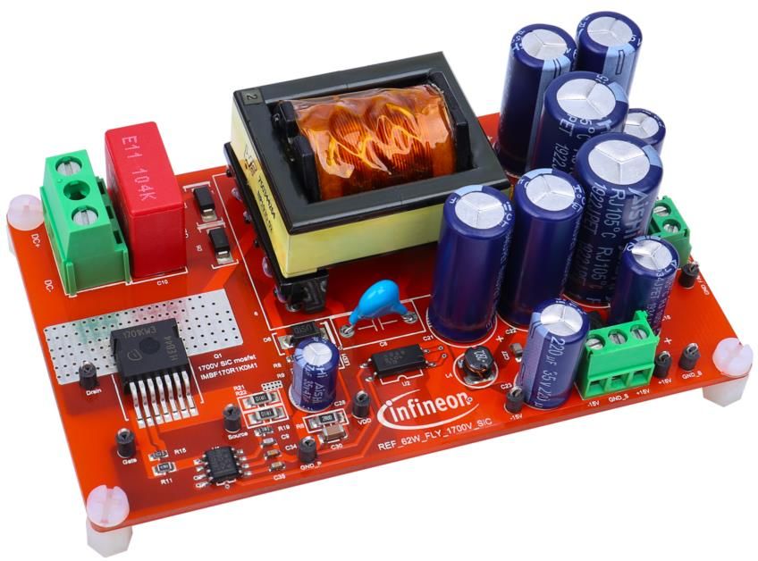
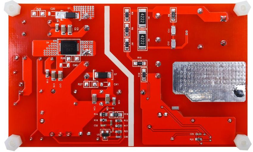
62.5W auxiliary power supply for three-phase power converter
Using the 1700 V CoolSiC™ MOSFET

4 Reference board specifications and descriptions
This section contains information about the reference board including the flyback transformer construction.

4.1 Board pictures
Figure 5 and Figure 6 show the top and bottom side of the reference board. The board has a size of 60mm x
100m x 25mm.
0

 1- Input voltage
 1
 VDC connector
 CN1
 2- Output voltage
 +/-15V
 connector CN2
 3- Output voltage
 4 +24V
 3
 connector CN3
 4- 1700V SiC
 MOSFET
 IMBF170R1K0
 2 M1

Figure 5 Top side of the reference board.

Figure 6 Bottom side of the reference board.

Application Note page 8 of 23 V 1.0
 2020-03-12

62.5W auxiliary power supply for three-phase power converter
Using the 1700 V CoolSiC™ MOSFET

4.2 The technical specification of board
The reference board is intended to support customers designing an auxiliary power supply for three-phase
converters using the Infineon 1700 V CoolSiC™ MOSFET. Potential applications includes solar inverters, energy
storage, EV-chargers, UPS and motor drives. Table 2 lists the key board specifications.

Table 2 Technical specification
 Input voltage 200 VDC to 1000 VDC
 Output power 62.5 W
 Topology Single-ended flyback
 Output voltage +24 V +15 V -15 V
 Tolerance 5% 2% 2%
 Output current 1A 2A 0.5 A
 Frequency 80 kHz, QR mode
 Derating of switches VDS 85% (1450 V)
 Efficiency at full load >85%

Application Note page 9 of 23 V 1.0
 2020-03-12
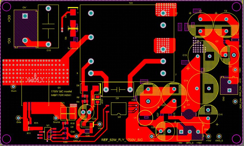
62.5W auxiliary power supply for three-phase power converter
Using the 1700 V CoolSiC™ MOSFET

4.3 Schematic
Figure 7 shows the schematic of the single-ended flyback converter for this reference board.

Figure 7 Schematic of the reference board.

Application Note page 10 of 23 V 1.0
 2020-03-12
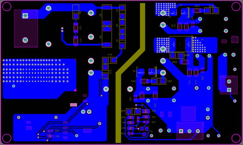
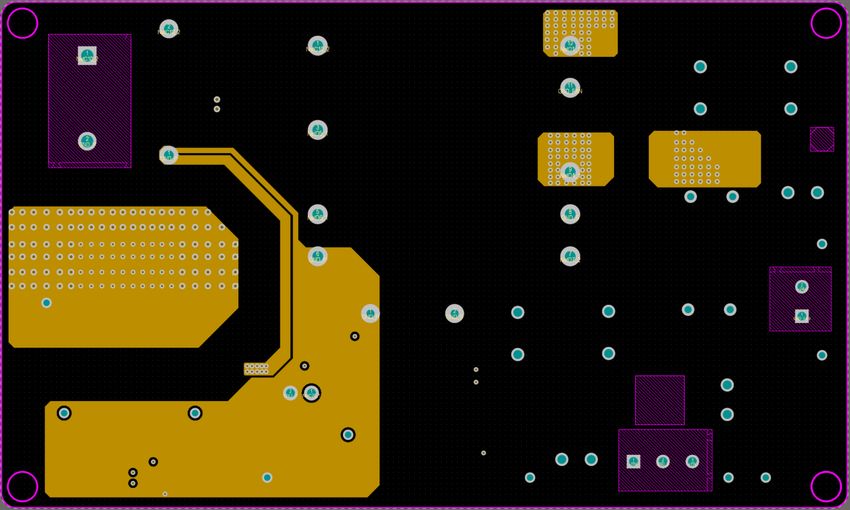
62.5W auxiliary power supply for three-phase power converter
Using the 1700 V CoolSiC™ MOSFET

4.4 PCB layout
The following pictures show the PCB layout and the component assembly marked with its respective
designators.

Figure 8 PCB top layer

Figure 9 PCB middle 1 layer
Application Note page 11 of 23 V 1.0
 2020-03-12
62.5W auxiliary power supply for three-phase power converter
Using the 1700 V CoolSiC™ MOSFET

Figure 10 PCB middle 2 layer

Figure 11 PCB bottom layer

Application Note page 12 of 23 V 1.0
 2020-03-12
62.5W auxiliary power supply for three-phase power converter
Using the 1700 V CoolSiC™ MOSFET

4.5 Bill of material
The BOM lists all components used for the PCB.

Table 3 Bill of material
Designator Description Part number Manufacturer Quantity
 -15V, +15V, TEST POINT PC 5002 KEYSTONE 10
 +24V, VDD, MINI .040"D WHITE ELECTRONICS
 GND_FAN,
 GND_P, GND_S,
 Gate, Drain,
 Source
 C1, C2, C21, C22 Electrolytic capacitor, 680uF, 20%, 35V ERJ1VM681G25OT Aishi 4

 C3, C16, C23 Electrolytic capacitor, 220uF, 20%, 35V ERJ1VM221F16OT Aishi 3
 C4, C5, C17, Ceramic capacitor, 10uF, X7R, 50V, C3216X7R1HK160A TDK 7
 C19, C24, C25, CAP1206
 C30
 C6, C7, C15, Ceramic capacitor, 1uF, X7R, 50V, 885012207103 Wurth 6
 C18, C26, C27 CAP0805
 C8 Y1 capacitor, 2.2nF, 500VAC, DE1E3RB222MN4AR01F Murata 1
 C9,C36 Ceramic capacitor, 100pF, X7R, 25V, 885012206053 Wurth 2
 CAP0603
 C10 Film Capacitor,100nF/1000V 890493425009CS Wurth 1
 C11, C12 Ceramic capacitor, 220pF, X7R, 1kV, CC1206KKX7RCBB221 Yageo 2
 CAP1206
 C13, C14 Electrolytic capacitor, 1800uF, 20%, ERJ1EM182W25OT Aishi 2
 25V
 C20, C40, C41 NC 3
 C28 Electrolytic capacitor, 47uF, 20%, 35V ERJ1VM470E09OT Aishi 1
 C29 Ceramic capacitor, 100nF, X7R, 50V, 885012206095 Wurth 1
 CAP0603
 C32 Ceramic capacitor, 1nF, X7R, 25V, 885012206059 Wurth 1
 CAP0603
 C33 Ceramic capacitor, 33nF, X7R, 25V, 885012206068 Wurth 1
 CAP0603
 C34 Ceramic capacitor, 390pF, X7R, 25V, C0603C391K3RACTU Kemet 1
 CAP0603
 C35 Ceramic capacitor, 10nF, X7R, 25V, 885012206065 Wurth 1
 CAP0603
 CN1 Horizontal entry with rising cage clamp 691216610002 Wurth 1
 WR-TBL, 2 pin
 CN2 Horizontal entry modular with rising 691214110003S Wurth 1
 cage clamp WR-TBL, 3 pin

Application Note page 13 of 23 V 1.0
 2020-03-12
62.5W auxiliary power supply for three-phase power converter
Using the 1700 V CoolSiC™ MOSFET

 CN3 Horizontal entry modular with rising 691214110002S Wurth 1
 cage clamp WR-TBL, 2 pin
 D1, D7 High voltage power Schottky rectifier MBR2150 Diodes 2
 D2 Schottky rectifier MBR0540 ONsemi 1
 D3, D5 1.0A surface mount ultra-fast rectifier US1M Diodes 2
 D4 Power Schottky rectifier STPS4S200 ST 1
 D6 1.0A surface mount ultra-fast rectifier US1D Diodes 1
 L1 WE-TPC SMT Tiny Power Inductor 744025003 Wurth 1
 L3 WE-TPC SMT Tiny Power Inductor 7440520018 Wurth 1
 L4 WE-PD2 SMD Power Inductor 744773022 Wurth 1
 LED1 LED RED CLEAR 0805 SMD 150080RS75000 Wurth 1
 Q1 1700V SiC MOSFET IMBF170R1K0M1 Infineon 1
 R1, R2 Resistor, 42.2k, 1%, RES2512 RC2512FR-0742K2L Yageo 2
 R3, R5, R7, R10, Resistor, 806K, 1%, RES1206 RC1206FR-07806KL Yageo 5
 R13
 R4 Resistor, 316R, 1%, RES1206 RC1206FR-07316RL Yageo 1
 R8 Resistor, 143k, 1%, RES0603 RC1206FR-07143KL Yageo 1
 R9 Resistor, 43k, 1%, RES0603 RC1206FR-0743KL Yageo 1
 R11 Resistor, 47R, 1%, RES0805 RC1206FR-0747RL Yageo 1
 R12, R20 Resistor, 10k, 1%, RES0603 RC1206FR-0710KL Yageo 2
 R14 Resistor, 1.2k, 1%, RES0805 RC1206FR-071K2L Yageo 1
 R15 Resistor, 4.7k, 1%, RES0603 RC1206FR-074K7L Yageo 1
 R16 Resistor, 1.3k, 1%, RES1206 RC1206FR-071K3L Yageo 1
 R17, R23 Resistor, 2.49k, 1%, RES0603 RC1206FR-072K49L Yageo 2
 R18 Resistor, 10.2k, 1%, RES0603 RC1206FR-0710K2L Yageo 1
 R19 Resistor, 2.15k, 1%, RES0603 RC1206FR-072K15L Yageo 1
 R21, R22 Resistor, 1R1, 1%, RES1206 RC1206FR-071R1L Yageo 2
 R25, R26, R27 NC
 TX1 flyback transformer 750344264-02 Wurth 1
 U1 Quasi-resonant controller UCC28600 TI 1
 U2 Long creepage photocoupler EL1013 Everlight 1
 U3 Precision programmable reference TL431BIDBZR TI 1

Application Note page 14 of 23 V 1.0
 2020-03-12
62.5W auxiliary power supply for three-phase power converter
Using the 1700 V CoolSiC™ MOSFET

4.6 Transformer construction
The flyback transformer was manufactured by Wurth. The following tables and figures shows key specifications
and information.

Table 4 Transformer specification
 Manufacturer and part number Wurth 750344264-02
 Core size ER28/17/11
 Core material DMR95
 Bobbin 12 pins ER28 vertical
 Primary inductance 772 uH measured from pin 1 to pin3 @100 kHz
 Leakage inductance
62.5W auxiliary power supply for three-phase power converter
Using the 1700 V CoolSiC™ MOSFET

Figures below depict the transformer setup and recommended land pattern.

Figure 13 Transformer setup diagram. Dimensions in brackets are in mm.

Figure 14 Transformer recommended land pattern. Dimensions in brackets are in mm.

Application Note page 16 of 23 V 1.0
 2020-03-12
62.5W auxiliary power supply for three-phase power converter Using the 1700 V CoolSiC™ MOSFET 5 Test results To demonstrate the high performance of the reference board with 1700 V CoolSiC™ MOSFETs, efficiency was measured accompanied with the switch voltage waveforms and thermal performance of the board. 5.1 Efficiency result Efficiency of the reference board was measured and test result is found in Figure 15, peak efficiency is 90.56% at a full load specification of 62.5 W with a gate resistor value of 47 . Figure 15 Measured efficiency versus DC input voltage. Test conditions: PO = 62.5 W and RG = 47 ohms. Application Note page 17 of 23 V 1.0 2020-03-12
62.5W auxiliary power supply for three-phase power converter
Using the 1700 V CoolSiC™ MOSFET

5.2 Waveforms
The next three figures show the drain-source voltage (VDS) and gate-source voltage (VGS) waveforms of the 1700V
CoolSiC™ MOSFET at different input voltage with full rated output load, and in these three waveforms, yellow
one is gate voltage VGS, purple one is drain-source voltage VDS.

Figure 16 Drain source and gate voltage at input voltage of 200 VDC

Figure 17 Drain source and gate voltage at input voltage of 800 VDC

Application Note page 18 of 23 V 1.0
 2020-03-12
62.5W auxiliary power supply for three-phase power converter
Using the 1700 V CoolSiC™ MOSFET

Figure 18 Drain source and gate voltage at input voltage of 1000 VDC

5.3 Thermal performance
By the nature of the reflow soldering process, there will be a certain number of voids in the solder joint, especially
on large-area pad, such as this TO263-7 package. One method to be considered when trying to reduce voids is
dividing whole big pad to small separated segments, segmentation of the stencil for exposed pads or other big
pads is shown in the following sketch, Figure 19.
With thermal through-holes (vias) and additional copper areas for heat spreading in inner layers of the PCB, an
improved thermal path from component to ambient is ready, and MOSFET will have an excellent thermal
performance without heatsink.

Figure 19 Example of a stencil design for a PG-TO263-7 package with and without vias in pad.

Application Note page 19 of 23 V 1.0
 2020-03-12
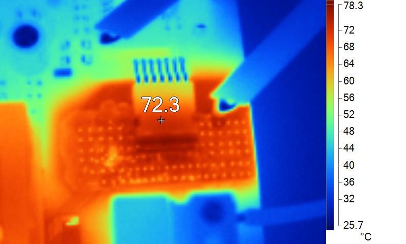
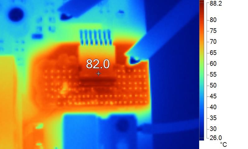
62.5W auxiliary power supply for three-phase power converter
Using the 1700 V CoolSiC™ MOSFET

The next three thermal images depict the thermal performance of the 1700 V CoolSiC™ MOSFET at different
input voltage with full rated output load and natural cooling at 25℃.

Figure 20 Thermal image at 600 VDC with full load

Figure 21 Thermal image at 700 VDC with full load

Application Note page 20 of 23 V 1.0
 2020-03-12
62.5W auxiliary power supply for three-phase power converter
Using the 1700 V CoolSiC™ MOSFET

Figure 22 Thermal image at 800 VDC with full load

Application Note page 21 of 23 V 1.0
 2020-03-12
62.5W auxiliary power supply for three-phase power converter
Using the 1700 V CoolSiC™ MOSFET

6 References
[1] IMBF170R1K0M1 datasheet, 1700 V CoolSiC™ MOSFET
[2] UCC28600 datasheet, 8-Pin Quasi-Resonant flyback Green-Mode Controller
[3] Gate resistor for power devices, Infineon Technologies, application note AN2015-06
[4] 62 W Auxiliary power supply for three-phase power converters using Infineon 1700 V silicon carbide
 MOSFET, PCIM Europe 2020

Attention: Infineon´s Product Registration is online now. Register your board and download more
 information

Three easy steps to register:
1. Go to www.Infineon.com/ login to my Infineon
2. Click on “Product Registration”
3. Choose your board and enter board series number, download the related information package

Revision History
 Page or reference Revision Date Description of change
 1.0 2020-03-12 Initial version

Application Note page 22 of 23 V 1.0
 2020-03-12
Trademarks
All referenced product or service names and trademarks are the property of their respective owners.

Edition 2020-03-12 For further information on the product, technology,
 delivery terms and conditions and prices please
 Published by contact your nearest Infineon Technologies office
 Infineon Technologies AG (www.infineon.com).
 81726 Munich, Germany
 WARNINGS
 Due to technical requirements products may contain
 © 2020 Infineon Technologies AG. dangerous substances. For information on the types
 All Rights Reserved. in question please contact your nearest Infineon
 Technologies office.
 Do you have a question about this
 Except as otherwise explicitly approved by Infineon
 document? Technologies in a written document signed by
 Email: erratum@infineon.com authorized representatives of Infineon
 Technologies, Infineon Technologies’ products may
 not be used in any applications where a failure of the
 Document reference product or any consequences of the use thereof can
 reasonably be expected to result in personal injury.
 AN2020-39
You can also read