Chapter 4: Medical, Health and Wearables - Heterogeneous ...
←
→
Page content transcription
If your browser does not render page correctly, please read the page content below
2020 Edition

                       Chapter 4: Medical,
                      Health and Wearables
                                   http://eps.ieee.org/hir

The HIR is devised and intended for technology assessment only and is without regard to
    any commercial considerations pertaining to individual products or equipment.
    We acknowledge with gratitude the use of material and figures in this Roadmap that are excerpted from original sources.
                    Figures & tables should be re-used only with the permission of the original source.
January, 2021                                                                                                                                   Medical, Health and Wearables
              Table of Contents
                                                                                                     To download additional chapters, please visit
                                                                                                                   http://eps.ieee.org/hir
   CHAPTER 1: HETEROGENEOUS INTEGRATION ROADMAP:
              DRIVING FORCE AND ENABLING TECHNOLOGY FOR SYSTEMS OF THE FUTURE
   CHAPTER 2: HIGH PERFORMANCE COMPUTING AND DATA CENTERS
   CHAPTER 3: THE INTERNET OF THINGS (IOT)
   CHAPTER 4: APPLICATIONS FOR MEDICAL, HEALTH AND WEARABLES
     EXECUTIVE SUMMARY ................................................................................................................................................................ 1
     INTRODUCTION ......................................................................................................................................................................... 1
     SCOPE ..................................................................................................................................................................................... 3
     DRIVERS AND EXAMPLES ............................................................................................................................................................. 3
     INTERCONNECT REQUIREMENTS ................................................................................................................................................... 6
     SUBSTRATE MATERIALS, TRACE FABRICATION, AND ASSEMBLY ........................................................................................................... 7
     EXAMPLES OF RECENT ADVANCES AND EMERGING TECHNOLOGIES ..................................................................................................... 9
     MATERIALS AND POWER ........................................................................................................................................................... 12
     CHALLENGES........................................................................................................................................................................... 12
   CHAPTER 5: AUTOMOTIVE
   CHAPTER 6: AEROSPACE AND DEFENSE
   CHAPTER 7: MOBILE
   CHAPTER 8: SINGLE CHIP AND MULTI CHIP INTEGRATION
   CHAPTER 9: INTEGRATED PHOTONICS
   CHAPTER 10: INTEGRATED POWER ELECTRONICS
   CHAPTER 11: MEMS AND SENSOR INTEGRATION
   CHAPTER 12: 5G COMMUNICATIONS
   CHAPTER 13: CO DESIGN FOR HETEROGENEOUS INTEGRATION
   CHAPTER 14: MODELING AND SIMULATION
   CHAPTER 15: MATERIALS AND EMERGING RESEARCH MATERIALS
   CHAPTER 16: EMERGING RESEARCH DEVICES
   CHAPTER 17: TEST TECHNOLOGY
   CHAPTER 18: SUPPLY CHAIN
   CHAPTER 19: SECURITY
   CHAPTER 20: THERMAL
   CHAPTER 21: SIP AND MODULE SYSTEM INTEGRATION
   CHAPTER 22: INTERCONNECTS FOR 2D AND 3D ARCHITECTURES
   CHAPTER 23: WAFER‐LEVEL PACKAGING (WLP)

HIR 2020 Version (eps.ieee.org/hir)                                                                                                     Heterogeneous Integration Roadmap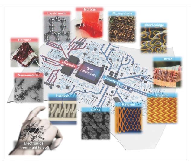
January, 2021                                                                            Medical, Health and Wearables

Chapter 4: Applications for Medical, Health and Wearables
Executive Summary                                                             Send corrections, comments and
   With increasing interest in miniaturization, there is a need for         suggested updates to the TWG chair,
packages that provide greater functionality in a smaller space. This            using our HIR SmartSheet:
technology roadmap recognizes miniaturization as a major driver in
consumer-electronics-based health monitors, diagnostics devices, and            https://rebrand.ly/HIR-feedback
aids, as well as implantable medical devices. While traditional
medical electronics remain conservative in the adoption of advanced packaging and assembly technology, the
emerging area of connected and distributed healthcare (including wearables attached directly to the skin) is in the
early stages, and many new materials and assembly methods are in development. The roadmap outlines today's
technology examples, including the materials and deposition methods, and discusses trends and challenges as the
technology moves forward. The roadmap recognizes the need for the integration of heterogeneous electronics in a
high-density design. Both 2D and 3D structures will continue in production. An increasing number of products will
also need to communicate and send data, balance power and thermal budgets, and are expected to drive the use of
radio systems. The roadmap for these devices is covered in the 5G/RF Communications chapter.
   There is increasing interest in wireless medical and health monitoring. The adoption and continued innovation in
flexible hybrid electronics is expected to drive this industry in the years to come. Miniaturization will drive the need
for packages that provide greater functionality in thinner and smaller spaces for both medical-grade- and consumer-
grade-based health monitors, as well as implantable and other medical devices. While traditional medical electronics
may remain conservative in design, the adoption of flexible hybrid electronics for wearables is attractive due to the
advantages in comfort and form factor. The integration of a variety of components and die (including thinned and
unpackaged processors, memory, sensors, MEMS, RF, optical, etc.) together with printed circuits on thin flexible
substrates will create the next generation of wearable medical systems. Many new materials, assembly methods and
applications are demonstrated in the literature. Prototypes are available for evaluation from a variety of companies.
The ability to integrate power sources (thin batteries, RF induction and energy harvesting), sensors (chemical,
electrical, optical and MEMS), RF (components and communications) and displays in thin flexible and comfortably
wearable formats will be critical. This chapter will describe these technologies, including target applications,
materials, deposition methods, components, device integration, and reliability; it will discuss trends and challenges
expected in the coming years. The following is an initial summary of flexible hybrid electronics applications for
medical, health and wearable technologies that are relevant to the progress needed over the next 10 to 15 years.
1. Introduction
   Medical and healthcare products including hearing aids – implantable devices such as pacemakers, defibrillators,
and neurostimulators, as well as portable monitoring systems such as a smart inhaler – are increasingly challenged
by the need for miniaturization. Miniaturization is a major driver in consumer electronics-based health monitors and
aids, as well as implantable devices and portable systems. Manufacturers of cardio implants, such as pacemakers and
defibrillators, and neurostimulators, cochlear implants, and insulin pumps are investigating the use of heterogeneous
integration to achieve the goals of smaller form factors with increased performance. Novel heterogeneous SiP
(System-in-Package) integration configurations enable these devices to meet user needs. MCPs (Multi-Chip
Packages) have been in production for a few decades, primarily for improved time-to-market and for critical
heterogeneous integration needs. A variety of package types are used, including lead-frame, wafer level packages
(WLP), fan-out WLP (FO-WLP), and laminate packages such as land grid arrays (LGAs) and ball grid arrays (BGAs).
Flex circuit is common across product types. Laminate substrates are also popular. Traditional interconnect methods
continue to include flip chip and wire bond while embedded die solutions, where interconnect is realized by plating,
are moving into production. New methods such as printed electronics and 3D printing are emerging. Roll-to-roll
and panel processing are being adopted. Low power is key for many applications, and new developments in battery,
battery management, and energy harvesting are needed. All these technologies have to be optimized for cost and at
the same time be sustainably compliant to an increasingly aware customer base as well as global environmental
legislations.
   Market studies and industry literature [1] describe sensors for medical wearable applications and a detailed
description of the currently available sensors, the application, the company that produces it, and its market
HIR 2020 versio (eps.ieee.org/hir)            Chapter 4, Page 1                     Heterogeneous Integration Roadmap
January, 2021 Medical, Health and Wearables
(regulatory) status. Examples include: Cefaly, a forehead wearable for migraine headache prevention; Backtrack
Skyn, a wrist wearable for blood alcohol monitoring; and CarePredict: Tempo, a wrist wearable ADL activity
monitor. Applications for maternal and neonatal care that include Ovulation Tracking and TempTraq baby
temperature monitoring are available. These devices are not limited to human use, and devices for veterinary
applications that include multiparameter sensors for respiration, heart rate, and distance are also available.
Representative Sensors for Medical Wearables typically include the following types:
ECG, PPG, Microphone, Inertial, Ultrasound, Electrochemical, Temperature, Pressure, EEG, and their
wearable formats for which they are available are presented in a tabulated list (i.e., wristband, patch,
headset, etc.)
Optical and Electrical Sensors are described for the detection of heart rate, cardiac function, blood
pressure, oximetry, and UV sensing.
Ultrasound Sensors for urinary incontinence.
Chemical Sensors for glucose monitoring, sweat, blood, and tears analysis
Microfluidics for analytes collection using MEMS-produced microneedles and micropumps
pH sensors in microfluidic patch and needle array formats
Pressure Sensors for blood pressure monitoring, respiratory monitoring and treatment (eg, sleep apnea),
gait analysis, and strain gauges for interocular pressure measurement (glaucoma).
MEMS microphones for use in hearing aids and cochlear implants.
Inertial Sensors for rehabilitation monitoring, activity tracking, and fall detection.
Dosage and fluid level counting.
Thermopiles for body temperature monitoring, especially for women's health (i.e., hormone changes).
Medical Wearables Supply Chain
This section describes the suppliers and manufacturers of sensors and systems that make up the wearables
ecosystem. These are strongly linked to IoT and mobility products and also require IT networks, cloud computing,
software, and AI developers. The ecosystem is evolving such that single sensor producers are working to develop
multisensory capability, and eventually devices with fully integrated multiplexed sensing, analysis, and
communications capability.
Challenges:
Current wearables such as activity trackers do not have sufficient accuracy to be used for medical
applications.
In the consumer market for medical wearables, the user is a consumer, not a patient, leading to variability
in device use and thus data.
Standards have not yet been set to ensure consumers, patients, and doctors can rely on data integrity across
many devices.
Mobile Phone applications are needed for use with smartphones capable of interfacing to new devices.
Data use acceptance within the medical community.
General Technology Trends:
Increasing miniaturization
Lower Power consumption and Energy production/harvesting
Increasing Accuracy
Increasing Connectivity
Shape, flexibility, and conformance improvements for wearability
Toward noninvasive skin wearable
From electrochemical toward optical sensing
Market studies [2] describe the global forecast for growth in the medical wearable device markets from 2018
through 2024. The report shows revenue growth, during this period, increasing from $7B to $32B. The sale of sensors
for medical device applications will dominate the growth with an increase over the period (of approximately 21.6%)
to $2.8B. In 2018 the dominant sensors were pressure and microphone units integrated into respiratory and hearing
aid devices. The largest growth areas will be devices for sensing respiratory and movement disorders, metabolic and
HIR version 1.0 (eps.ieee.org/hir) Chapter 4, Page 2 Heterogeneous Integration Roadmap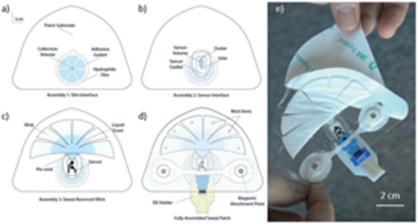
January, 2021 Medical, Health and Wearables
cardiovascular monitoring, blood glucose level monitoring, and drug delivery. These will be primarily incorporated
in banded wearable devices such as smartwatches. Such applications are enabled by shrinking size and increased
functionality of microelectronic sensors capable of near-field wireless communication to increasingly ubiquitous
smartphones, which in turn are able to easily connect to the internet. This provides a grand scheme of interconnection
for data transmission in support of medical monitoring and diagnostics.
Currently, no wearable products with high conformability and flexibility have successfully reached the market,
although this is indeed the goal. The majority of currently marketed wearables are for fitness monitoring including
heart rate, activity, sleep quality, and temperature, and are incorporated into wrist-worn (89%) smartwatches.
Developers are focusing on multiplexed sensing devices that integrate multiple sensing capabilities (with lowest
power consumption and added energy harvesting) into flexible and conformal (e.g., skin wearable) packaging
formats. These will require the development of thin and flexible sensor, logic, memory, and battery components.
Currently, many new and novel sensors are under development such as those for sleep apnea, oxygen diffusion to
track wound healing, and for chemical analysis of biofluids such as sweat, saliva, blood, and tears.
Limitations in the use of wearable medical devices include high cost, incompatibility across all smartphone
operating systems, and a lack of data format standards. Devices must not only be comfortable, but also their proper
use is dependent upon the wearer and as such are prone to variable responses. There is also a lack of understanding
by medical professionals relating to how to acquire, utilize, and interpret data. In terms of device vetting, there is
also a lack of available data supporting their safety, accuracy, reliability, and effectiveness, all necessary for the
establishment of regulatory standards for their manufacture, performance and use. As evidence, very few Class II
and Class III flexible wearable medical devices have been approved for sale in the US due to the need to meet ISO
standards and gain FDA approval. These approvals can delay marketing of a medical device significantly. In the US
the typical time (delay) required for launching a new medical device due to these approval requirements is 1-3 years,
compared to a much shorter (typical) 45-day delay for marketing non-medical consumer electronics. For globally
marketed products, even more regulations may apply.
2. Scope
This roadmap chapter has a two-fold purpose:
Define products and their packaging requirements.
Examine materials and package trends, including substrate materials and features.
Analyze new manufacturing trends such as flexible manufacturing with printed electronics.
Devices continue to be populated with a wide variety of sensors such as air quality particle counters,
humidity, temperature, pH. Currently several of these sensors are discrete and need individual assembly to
the substrate i.e., PCB. This drives the size of the smart device larger than the predecessor. Miniaturization
and integration structure that do multi-modal sensing will help enable smarter but thinner devices.
The chapter is organized into three primary areas:
Product examples including the substrates, devices, interconnect methods, and packages
Substrate trends
Manufacturing trends
Challenges
3. Drivers and Examples
"Nanopackaging for Component Assembly and Embedded Power in Flexible Electronics: Heterogeneous
Component Integration for Flexible Systems" [3] describes which applications and products drive the growth of
flexible and printed electronics. Drivers typically include flexible displays, aviation and automotive, wearable health
and medical devices, bioelectronics, and devices for IoT. The functions of a flexible package may include sensing,
computing, communication, and power management. Flexible electronics have requirements different from
traditional print-and-etch rigid PWB electronics. They require:
Flex Substrate: supports wiring and components
Interconnection and component assembly: Flexible conductive adhesives, flexible (eg, nano copper)
interconnects, new assembly technology i.e. thinned die pick and place, lower temperature solders
Flexible power supplies/batteries/energy harvesting: solar, piezoelectric, thermoelectric, inductors, pyro-
and triboelectric
HIR version 1.0 (eps.ieee.org/hir) Chapter 4, Page 3 Heterogeneous Integration Roadmap
January, 2021 Medical, Health and Wearables
Printed discrete elements including flexible capacitors and inductors
General trends and expectations include:
Flexible electronics typically require all components of the system be flexible.
Majority of flex substrates are organic, and hence processing and applications are limited to lower
temperatures.
Commercial economic viability requires existing manufacturing infrastructure be adapted to fabricate these
electronics.
Materials for printing electronics on substrates are deficient in electrical properties compared to traditional
materials i.e. lower-conductivity conductors, higher dielectric constant dielectrics.
Inferior adhesion and materials (if used) mean lower resistance to stressing, and hence lower thermal and
mechanical reliabilities.
Energy storage capacity and power delivery is deficient compared to traditional devices. Conventional
batteries and semiconductors do not perform as expected when stretched or bent, thus developments in
materials and their combined usage are required here.
Flexible electronics cannot currently match the transistor density of traditional rigid electronics. Hence, the
requirement for flexible hybrid electronic devices.
Medical and healthcare products including implantable devices such as pacemakers, defibrillators, and
neurostimulators, insulin pumps, hearing aids and cochlear implants, as well as portable image and monitoring
systems such as smart inhalers, air quality monitors, continuous glucose monitors, and point-of-care diagnostic
devices are increasingly challenged by the need for miniaturization. Miniaturized packaging for many sensor and
human-machine interface (displays, radios) applications is required for healthcare products, including biometric
sensors. Sensor and communication gateway and power use is expected to increase. Heterogeneous integration of
electronics in a high-density design is required to not only reduce size but to integrate performance and reduce power
consumption. An increasing number of products will need to communicate and send data, driving the use of radio
systems that will also be in the form of heterogeneous integration.
Medical devices that are permanently implanted or used within the body for limited periods are constrained by
considerations of the biocompatibility of the surfaces, hermeticity, and toxicity of construction materials. In many
cases, the strength and rigidity or flexibility of the structure may be important for long term use. Surfaces in contact
with tissue are often coated to minimize inflammatory responses and to prevent tissue damage. These considerations
are application dependent and must be taken into account during the earliest stages of the design process, and will
guide solution pathways, often requiring different materials than used in standard consumer electronics.
Medical implantable devices such as pacemakers have decreased in size, from when the first pacemakers were
introduced as external units in 1957 to implantable devices that required surgery, and now to small leadless products
that are a fraction of the size and do not require surgery. Both Abbott's (formerly St. Jude) Nanostim and Medtronic's
Mica are delivered to the heart via a catheter snaked up through the femoral artery. Medtronic indicates its pacemaker
required extremely dense electronics packaging. The integrated circuits are very thin and are stacked on top of each
other and packaged in a very dense module. The laminate substrate is ultra-thin. The pacemaker has wireless
functionality, so Medtronic redesigned its own wireless antenna integrated into the device. ECGs are also expected
to use SiP. A prototype flexible hybrid electronics module 2-inches by 2-inches has been developed by i3Electronics
to wirelessly monitor EEG output through a surface-mounted Bluetooth module attached to a patient. Modules
include 8-channel (12 bit) analog-to-digital converters, SRAM, and flash memory. Examples of other technologies
include:
Neurostimulation modulation requires small form factor electronics, and many new packaging
configurations are under investigation. [4] A typical product may contain two die and 100 passive
components. These devices are mounted on a PCB substrate. Die sizes are typically 7 mm x 7 mm and
include a transceiver. The requirements for neural stimulation probes include biocompatibility and
hermetic connections. Implants under the cranium (skull) must be low power and highly efficient to
prevent brain fluid temperature changes. [5] For long-term implant stability and to avoid scar tissue
formation, the probes should have mechanical properties and surface chemistry similar to the surrounding
tissue. [6]
HIR version 1.0 (eps.ieee.org/hir) Chapter 4, Page 4 Heterogeneous Integration Roadmap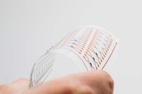
January, 2021 Medical, Health and Wearables
Smaller Cochlear implants that require miniaturization of electronics are under development. Pill cameras
also need high-density packaging, including stacked die, to meet form factor requirements. In one
example, three flip chip die and 96 SMT are mounted on the substrate and encapsulated. A full RF module
contains five components (Transceiver, SAE filter, crystal, ferrite, and diode) plus an integrated passive
device.
Balloon catheters with electrodes for neurostimulation or ablation use extremely flexible ultra-thin two-
layer liquid crystal polymer film (LCP) build-up with 50µm thickness. There is one thermistor per
electrode, coupled with the thin film layers. The LCP has 25µm lines and spaces and one-sided Cu plating
with 100% via-fill. The surface finish is electroplated gold on Cu for a short-term implant.
Ultrasound imaging products typically use off-the-shelf components instead of custom devices. Devices
include analog, digital signal processors (DSPs), and field programmable gate arrays (FPGAs). Ultrasound
modules have been fabricated using 14µm line and space single-sided flex with 11µm line and space
double-sided flex with 25µm through vias.
Hearing devices (hearables) include ear buds, hearing aids, and Cohclear implants. Devices include MCU,
audio CODEC, switches, battery chargers, Flash memory, amplifiers, controllers, and digital signal
processors. Hearing aids originally used ceramic substrates, but many have transitioned to include FR-4 or
BT-resin for the rigid circuit and flex circuit. In some cases, the flex circuit is folded, and multiple die are
attached. Bending zones have interconnects between different assembly portions. Low loss dissipation is
required for the substrate. Often an integrated electromagnetic shielding is used.
SiP formats include embedded die in Cu-polyimide flex circuits. In one structure the thinned die is embedded in
an adhesive-based polyimide film flex circuit with Cu features. Conductive paste is used for via connections. The
die are prepared for embedding with a fan-in RDL WLP process. Examples in production include embedding of a
single die with 5 to 9 wiring layers with a total thickness of 280 to 500 µm and a two-die stack with 10 to 13 wiring
layers and a thickness of 580 to 700 µm. In the future, three-die single stacks and two stacks will be in production.
There will be 14 to 16 wiring layers and the thickness will be 800 to 980 µm. The module size will be 9.9 mm x 6.6
mm x 0.85 mm with for the two stacks of three die each. The embedded die size is 3.2 mm squared, and the I/O pitch
of the embedded chip is 0.4 mm [7].
Embedded subsystems in substrates for medical applications also include insulin pumps, cochlear implants, and
cardiac implants. A two-layer SiP was fabricated with 35µm copper line spacing using a semi-additive process, and
many fine blind and through vias were fabricated. Die stacking processes have been demonstrated. In one example
the module was only of 3.48 mm x 3.48 mm x 1.5 mm [8]. Applications include:
A Cochlear implant fabricated with LCP as a biocompatible material without copper for a long-term
implant. Features are 125µm traces on 250µm pads and structures have 15µm lines and spaces. Au and Pt
are used for electrodes. Au is used for good adhesion and flexible properties. The implant uses 90% wires
of platinum and 10% iridium. Up to 24 wires are connected to an audio processor. The electrode array and
coil are injected with silicone and cured. The final device is housed in a titanium block.
A short-term embedded blood glucose sensor is embedded for 30 days in the human body and measures
capacitive electric current charge; it is typically a three-electrode system with a counter electrode, a
reference electrode, and a work electrode.
Smartwatches and fitness bands are a wearable that may or may not be classified as medical devices.
Devices in these products include Flash and DRAM, controllers, an RF front end module (FEM), heart rate
sensor, application processor with modem, power management IC (PMIC), WiFi, Bluetooth, NGSS
receiver, antenna switch, USB switch, and Hall Effect sensor.
Point-of-case diagnostic and drug delivery devices include MCU, audio CODEC, switches, battery chargers,
Flash, amplifiers, controllers, displays and digital signal processors. They also include sensors for air quality, sweat,
humidity, temperature, motion, Hall, proximity, contact, mechanical operation, and counter sensors. Several of these
platforms may end up on flexible substrates made of PET or thermoplastic polyurethane (TPU). Increasing
integration but minimizing heat dissipation will be critical in such applications. The terminations of such devices
will also have to consider the potential for assembly on silver ink traces with conductive adhesives or extremely low
temperature solders.
Stretchable and printable medical electronics, including textiles, are in the early stages of development and in
some cases the devices are printed and in others the devices are attached using adhesives or surface mount technology
HIR version 1.0 (eps.ieee.org/hir) Chapter 4, Page 5 Heterogeneous Integration Roadmap
January, 2021 Medical, Health and Wearables
(SMT). In some cases, the electrodes are screen printed on (TPU film substrates and bonded to a textile by a hot melt
adhesive. Silver micro-flakes are mixed with a TPU film and heat-cured to make a stretchable fabric. In some cases,
the width of the line is 520 µm and the space is 480 µm [9].
Sensors attached directly to the skin are increasingly used to monitor health, athletic performance, and muscle and
nerve conditions. Sensors placed on a fingernail are in development. A wearable fingernail deformation sensor
system uses a 40 µm thick silicon strain sensor, a three-axis accelerometer, and an RF module to transmit the signal.
Handle tape is used to attach the silicon layers [10].
Many new developments are taking place in smart textiles in many organizations, including universities and start-
ups. For example, Carnegie Mellon University researchers have developed a self-healing circuit material that can
repair itself. The material is composed of liquid metal droplets suspended in a soft elastomer. This is the foundation
of the self-repair process. The material can be used in self-healing electrical circuits, which when produced with
conductive traces of this material, remain fully and continuously operational if severed or punctured [11]. In another
example, researchers at the University of California San Diego have fabricated a stretchable electronic patch with
wireless monitoring that can be worn on the skin, similar to a bandage.
A sensor patch system has been fabricated using a Tegaderm polymer film with a Cu sensor electrode fabricated
on it. The sensor patch is placed over a cannula needle inserted into the patient's vein for drug or fluid delivery to
detect skin swelling. The sensor electrode pattern is laser machined onto a 400µm thick silicon wafer, and the
polymer film is attached to the back of the stencil wafer and a sputtering process is used to pattern the sensor electrode
and pad. The first layer of metal is Ti, acting as an adhesive layer between the second metal layer, Cu, and the
polymer film. The 2µm Cu layer is sputtered, followed by a thin (200 angstroms) layer of Au (to act as a passivation
layer). The conductors are attached with double-sided conductive film [12].
Embedded die are used for other sensor applications. Assembly of ultra-thin die on flexible substrates is
challenging. In one example, a small, thin die is embedded in a flexible substrate using a FO-WLP process with fine-
pitch wiring. Small 2.5mm x 2.5mm die with 100µm thickness are embedded. Devices include photodiodes and a
micro-LED driver. The structure can be mounted on a curved human fingernail and used for trans-nail pulse wave
monitoring [13]. In another approach, a thinned die is embedded using a highly flexible elastomeric molding
compound, polydimethylsiloxane (PDMS), using a FO-WLP process. This embedded substrate approach allows a 2
mm bending range. Foldable displays have been demonstrated, and the technology can be used for multi-channel
surface electromyography systems or optogenetics for neural implants [14]. Other examples include the following:
Wireless, implantable, stretchable biosensor systems have been developed, comprised of a miniaturized
capacitive sensor and inductive coil without a battery. In some cases, the capacitive sensor is fabricated
using aerosol jet printing of silver nanoparticles and polyimide. Silicone elastomer is used to encapsulate
the sensor prior to conformal integration onto a medical stent [15].
Examples of heterogeneous integration include the fabrication of an ECG monitor with a
microcontroller/Bluetooth, antenna, ECG electrodes, analog front-end on a 2-inch x 2-inch polyimide
substrate with 64 plated Cu through holes. Capacitive electrodes are formed by alternate deposition of 166
layers of Al2O3 and TiO2. The total thickness is 103 nm, the dielectric constant is 120, and 0.53
microF/cm2 [16].
A wearable passive pH sensor for health monitoring consisting of Ag/AgCl and Sb/Sb2O3 electrodes and a
transponder consisting of an RF front end and an antenna has been fabricated. The electrodes are
fabricated and connected to Cu pads on a 380µm thick PTFE substrate. The sensor tag and transponder are
integrated into a mouthguard. An energy-harvesting method is used instead of a battery to power the system
[17].
Ultra-small passive devices are used in a variety of products. In some cases, integrated passives are used.
Examples include Murata's IPDIA used for pacemakers, medical sensors, and brain stimulation.
4. Interconnect Requirements
Wire-bond interconnects continue to be used in some applications for connections between die and package or
board. Au wire is most common. An increasing number of products require 3D integration to achieve desired form
factors. The 3D integration can take the form of stacked die with wire bonds. Within-Package Interconnects enable
lateral connections between two nodes or electrodes. Package-to-Board Interconnects are between the package and
the next level, typically the motherboard, and are referred to as the second level interconnect (SLI).
HIR version 1.0 (eps.ieee.org/hir) Chapter 4, Page 6 Heterogeneous Integration RoadmapJanuary, 2021 Medical, Health and Wearables Wafer level packages (WLP) and flip chip interconnect are also increasingly used in consumer wearables. The number of WLPs in smartwatches and fitness products continues to increase from none to a few in early products to four to nine in fitness bands and as many as 27 in today's smartwatches with health or medical functions. The number of WLPs in a smartwatch has increased from 18 to 27, for the highest-end modes. Many of these are found inside the SiP. Fan-out WLPs with multiple die are also being adopted. These are considered examples of heterogeneous integration. Increased use of SiPs is expected in formats that include wire bond, flip chip, and WLP. Driven by miniaturization, functionality, and durability, SiPs may take the form of embedded die. Flip chip continues to be used for a variety of products ranging from hearing aids and pacemakers to smartwatches. Typically, the flip chip devices are
January, 2021 Medical, Health and Wearables
additively deposited noble metals (such as Au or Pt) are used as surface finishes and for implantable (electrode)
applications.
Plated metal circuits on lower-cost substrates such as PET (see the
picture on the right) will emerge as a compromise between
conductivity and cost in certain applications.
Wearable electronics in the form of implanted or skin-attached
products are in development, but the work is still in the early stages.
TPU, polyimide (Kapton and Upilex), and PET are being used for
skin patches.
The terminations of devices on such substrates will also have to
consider the potential for assembly on silver ink traces with conductive
adhesives or extremely low temperature solders.
Knitting or weaving conductive threads into textiles is under development with Ag, Cu, Sn, or Ni alloy
metalized threads. Coating or deposition of conductive polymers is under investigation.
Conductors (typically inks) are deposited by aerosol jet, inkjet, or screen printing. Features of 10 µm line and
space have been fabricated. Inkjet droplets (pico-liter in volume) can be jetted by thousands of individually
addressable nozzles at the same time and are deposited in a non-contact manner. Inkjet printing is proposed as a low-
cost direct patterning method to provide higher resolution than weaving. Inkjet printing for semiconductor packaging
applications requires higher accuracy and reliability than today's inkjet printer technology. It requires the use of piezo
driven heads used in large-scale graphics printers. A high-precision motion platform, precise pattern rendering,
modular design, head inspection, and easy maintenance are required. These requirements add cost to a semiconductor
inkjet system, but the total cost is significantly less than the BEOL lithography in use today. Other advantages to
inkjet printing for BEOL include quick change of pattering (digital printing), efficient use of materials (fewer
subtractive processes, if any), ability to handle larger-area substrates (panel size), and significant cost reductions
(compared to lithography). Inkjet printing can be used to fill vias, trenches, and cavities from a micron to a millimeter
in thicknesses.
Inkjet materials will be critical to the success of applying printed electronics to BEOL technologies. Materials
come in several groupings: dielectrics (such as polyimide), fast-curing UV polymers, resists for etch or plating
masking, and conductive inks. The most popular of the conductive inks are Cu and Ag nanoparticle suspensions in
solvents that cure below 150°C. Ink materials must have viscosities in the 2-20 centipoise (cP) range, controlled
surface tension, and uniform particle sizes and particle loading. Future ink materials could include special adhesives,
graphene, quantum dot ink, sensor materials, optical sensors, biomaterials, and passive component materials (resistors
and capacitors). Carbon nanotube (CNT) is also under investigation.
Inks can be printed at room temperature and take about 15 minutes to dry. There is no need to pause the deposition
process for the ink to dry. Layers can be printed one over another while curing, with no effect on the final material's
properties. New inks continue to be developed that can improve the performance and manufacturability of printed
electronics. Cu paste for screen printing has been developed that provides high adhesive strength to glass, PET,
polyimide, FR4, and ITO, and high conductivity of 20 to 30 microOhm/cm using a low-temperature (120°C) sintering
process; some Cu inks require a reducing atmosphere for sintering. It is capable of printing 50µm lines/spaces. It is
targeted to replace Ag paste in applications. Black phosphorus, a two-dimensional material similar to graphene, has
been incorporated into an ink that is compatible with conventional inkjet printers. The material can be printed on
silicon, so it can be used to make transistors or photodetectors. It could be printed on plastic and used to make flexible
displays, or on glass for transparent devices. While not as conductive as graphene, black phosphorus is believed to
be sensitive to a greater region of the electromagnetic spectrum, including infrared, making it suitable for the
development of optoelectronic devices including solder cells, light emitters, optical fibers, and sensors [18].
Inkjet printing of electrodes on paper and then transfer as a temporary tattoo has also been reported. Silver-
flake ink has been used [19].
One of the challenges is printing on a rough and porous surface; therefore, coating an interface layer on
fibrous substrates before printing is being proposed. A polyurethane-based ultraviolet curable paste has
been proposed as an interface layer to fill pores in textiles and improve surface roughness before an antenna
is printed. Ag nanoparticle inks have been demonstrated [20].
HIR version 1.0 (eps.ieee.org/hir) Chapter 4, Page 8 Heterogeneous Integration RoadmapJanuary, 2021 Medical, Health and Wearables
More conventional methods of component attachment to flexible circuits have also been proposed. Circuits
have been mounted with SnBiAg or SAC305 solder on Cu clad stretchable material [21].
Anisotropic conductive adhesive film (ACF) has been demonstrated to provide good electrical connections
with a low-temperature process. In one example, 50µm thick silicon chips with Cu/Ni/Au bumps using
ACF and thermo-compression bonding were attached to a substrate. The Cu-patterned polymer flexible
substrate uses a polyester/rayon woven fabric with a 12µm thick Cu foil and 40µm thick B-stage adhesive
(styrene-isoprene-styrene block copolymer elastomer) added during fabrication. Stable joint resistance has
been reported after 12mm radius convex and concave bending [22]. Companies are also investigating and
moving into production with flip chip attached to PET flex circuits using ACA and advanced z-axis
materials.
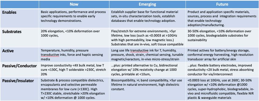
Summary of Trends in Materials for Flexible Hybrid Electronics
Trends in Device, Integration, Packaging and Assembly of Flexible Hybrid Electronics
Now Emerging Future
Enables Thinned die and compliant assembly Clothing/textile substrates for wearable Embedded components and integrated
methods. Stretchable and conformal applications. Printed features for RF and hi‐ passives. Encapsulation for harsh
substrates. Flexible low dielectric and speed function. Flexible interposed for fine‐ environments. From sheets to roll based
low loss RF materials. pitch die attach device assembly.
Circuitization Low I/O (200µm) for Flexible substrates w/ stretchable circuitry, Multi‐layer flex circuits w/ internal
controllers, memory, communication w/ RF materials, textile substrates power/ground, vias and embedded
compliant chip attach function. Printed conductors,
transmission lines, dielectrics, vias RCL,
sensors and 3D features
Non‐printed Thin die flip‐chip bonding Flexible interposer for fine‐pitch,January, 2021 Medical, Health and Wearables
The device facilitates healing without removing the bandage and has the potential to change the way diabetic wounds
are treated [24]. A similar effort was conducted at Purdue and supported by NextFlex.
"A Wearable Electrochemical Platform for Noninvasive Simultaneous Monitoring of Ca2+ and pH" [25] describes
wearable and disposable PET flex for concurrent pH, temperature, Ca+2 sensing. Sensor Flex is interfaced to a
concurrently worn rigid circuit board that enables selective real-time quantitative analysis and wireless transmission
of Ca+2 in body fluids such as sweat, tears, and urine with pH and temperature correction.
"A wearable patch for continuous monitoring of sweat
electrolytes during exertion" [26] is the demonstration of a
fully integrated, wireless, wearable, and flexible sweat
sensing device for non-obtrusive and continuous
monitoring of electrolytes during moderate to intense
exertion as a metric for hydration status. The focus of this
work is two-fold: 1) design of a conformable fluidics
system to suit conditions of operation for sweat collection
(to minimize sensor lag) with rapid removal of sweat from
the sensing site (to minimize effects on sweat physiology).
2) integration of Na+ and K+ ion-selective electrodes
(ISEs) with flexible microfluidics and low noise small footprint electronic components to enable wireless, wearable
sweat monitoring. While this device is specific to electrolyte analysis during intense perspiration, the lessons in
microfluidics and overall system design are likely applicable across a broad range of analytes. The device is
composed of a flexible disposable sensor/microfluidics module and a reusable electronics module. Key challenge:
clinical acceptance. Potential shortcoming: not accurate at low perspiration rates.
"Flexible Electronics toward Wearable Sensing" [27] is a summary of recent studies on the design of flexible
electronic devices and systems for chemical and physical monitoring. It discusses material innovations, sensor
design, device fabrication, system integration, and human studies employed toward continuous noninvasive wearable
sensing.
"Battery-free, stretchable optoelectronic systems for wireless optical characterization of the skin," [28] introduces
active optoelectronic systems that function without batteries and in an entirely wireless mode, with examples in thin,
stretchable platforms designed for multiwavelength optical characterization of the skin. Magnetic inductive coupling
and near-field communication (NFC) schemes deliver power to multicolored light-emitting diodes and extract digital
data from integrated photodetectors in ways compatible with standard NFC-enabled platforms, such as smartphones
and tablet computers. Examples in the monitoring of heart rate and temporal dynamics of arterial blood flow, in
quantifying tissue oxygenation and ultraviolet dosimetry, and performing four-color spectroscopic evaluation of the
skin demonstrate the versatility of these concepts. The results have potential relevance in both hospital care and at-
home diagnostics.
"Highly flexible, wearable, and disposable cardiac biosensors for remote and ambulatory monitoring" [29] reports
on advancing contemporary cardiac and heart rate monitoring devices that capture physiological signals using optical
and electrode-based sensors. However, these devices generally lack the form factor and mechanical flexibility
necessary for use in ambulatory and home environments. It reports an ultrathin (~1 mm average thickness) and highly
flexible wearable cardiac sensor (WiSP) designed to be minimal in cost (disposable), lightweight (1.2 g), water-
resistant, and capable of wireless energy harvesting. Theoretical analyses of system-level bending mechanics show
the advantages of WiSP's flexible electronics, soft encapsulation layers, and bio-adhesives, enabling intimate skin
coupling. A clinical feasibility study conducted in atrial fibrillation patients demonstrates that the WiSP device
effectively measures cardiac signals matching the Holter monitor and is more comfortable. WiSP's physical attributes
and performance results demonstrate its utility for monitoring cardiac signals during daily activity, exertion, and
sleep, with implications for home-based care. The WiSP device is comparable in size to a standard adhesive bandage
(58 mm × 25 mm × 1 mm) and streams physiological data to commercial smartphones via standard near-field-
communication (NFC) for use in both ambulatory and home-based settings.
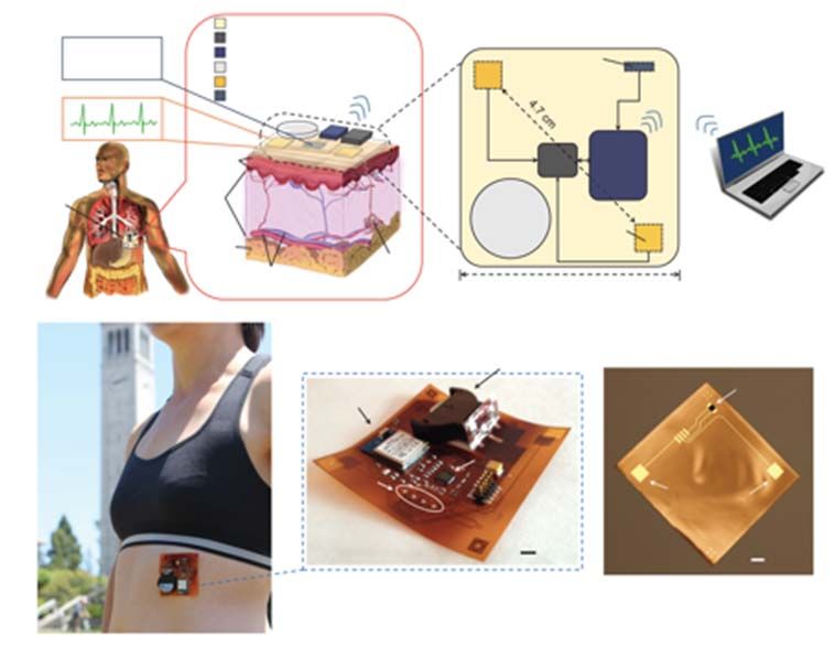
"Flexible Hybrid Electronics: Direct Interfacing of Soft and Hard Electronics for Wearable Health Monitoring"
[30] describes interfacing of soft and hard electronics as a key challenge for flexible hybrid electronics. Here, a single
substrate interfacing approach is reported, where soft devices, i.e., sensors, are directly printed on Kapton polyimide
substrates that are widely used for fabricating flexible printed circuit boards (FPCBs). Utilizing a process flow
compatible with the FPCB assembly process, a wearable sensor patch is fabricated using inkjet‐printed gold
HIR version 1.0 (eps.ieee.org/hir) Chapter 4, Page 10 Heterogeneous Integration RoadmapJanuary, 2021 Medical, Health and Wearables
electrocardiography (ECG) electrodes and a stencil‐printed nickel oxide
thermistor. The ECG electrodes provide 1 mVp-p ECG signal at 4.7 cm
electrode spacing, and the thermistor is highly sensitive at normal body
temperatures and demonstrates temperature coefficient, α ≈ –5.84% K–
1
and material constant, β ≈ 4330 K. This sensor platform can be
extended to a more sophisticated multi-sensor platform where sensors
fabricated using solution-processable functional inks can be interfaced to
hard electronics for health and performance monitoring, as well as
internet of things applications.
New stretchable electronic patches could transform rehabilitation and
long-term care [31]. Prof. John A. Rogers at Northwestern University is
developing a wearable patch that could record acoustics within the body,
such as sounds within a joint or vibrations from speech. The goal was to build a soft, wireless, skin-interfaced device
with the form factor of a bandage and the functions of a stethoscope to continuously and precisely measure the body's
subtle mechanical and acoustic signatures. The result yielded a real diagnostic and treatment tool to measure a
rehabilitating stroke patient's patterns of speech and swallowing. The result, the first wearable device designed for
the throat, is a "much more personalized, quantitative approach to rehabilitation.” The throat sensor is just one in a
portfolio of innovations developed in Northwestern's Center for Bio-Integrated Electronics. Rogers and his
collaborators have developed materials and design approaches that transform electronics from traditional rigid silicon
circuits into soft, conforming, thin devices that integrate with the body while transmitting real-time information
wirelessly to both physicians and machine-learning algorithms that can find new patterns within data.
The team has also developed devices that can be worn on the body to measure sweat rate and chemistry, or to
quantify exposure to solar UV radiation, as well as devices that can be implanted within the body to harvest energy
from organs and automatically treat abnormal heart conditions. “The patch had to be constructed so that people forget
it's there once they put it on," Rogers was quoted: "We strive on the engineering and materials side to make it fully
skin-like and physically imperceptible."
In "Smart Skin - Electronics that stick and stretch like a temporary tattoo" [32], engineers developed a device
platform that combines electronic components for sensing, medical diagnostics, communications and human-machine
interfaces, all on an ultrathin skin-like patch that mounts directly onto the skin with the ease, flexibility and comfort
of a temporary tattoo.
Application Roadmap for Wearable Flexible Hybrid Electronics
HIR version 1.0 (eps.ieee.org/hir) Chapter 4, Page 11 Heterogeneous Integration RoadmapJanuary, 2021 Medical, Health and Wearables
7. Materials and Power
"Materials and Structures toward Soft Electronics" [33] presents a comprehensive discussion of the strategies in
materials innovation and structural design to build soft electronic devices and systems on non-planer surfaces. For
each strategy, the presentation focuses on the fundamental materials science and mechanics, and example device
applications are highlighted where possible. Finally, perspectives on the key challenges and future directions of this
field are presented.
The implications of soft electronics integrating with nonplanar objects are multifold. First, the intimate contact
between the device and the nonplanar object will allow high‐quality data to be collected. With rigid electronics, air
gaps at the interface between the device and the object reduce the contact area, and can potentially introduce noise
and artifacts, which compromise signal quality. Second,
foldable, low‐profile devices can enable mobile and
distributed sensing, which hold great promise for
Internet‐of‐Things technology. Finally, in the area of
medical devices, which is probably the major driving
force of this field at present, soft electronics have similar
mechanical properties and thus cause minimal irritation
to the human skin, which can be a key enabling
technology for continuous healthcare.
Two strategies can be applied to achieve stretchability
in electronics: 1) materials innovation, by developing
novel materials that are stretchable in single or
aggregated forms; 2) structural design, by making non-
stretchable materials into specific structures that can
absorb the applied strain without fracturing, e.g., by
inducing mixed modes of mechanical deformations. In
this review, we summarize state‐of‐the‐art advances in
both strategies, covering a broad range of topics (see
figure), including hydrogels, liquid metals, conductive polymers, and nanomaterials for the material approach, and
waves/wrinkles, "island–bridges," textiles, origami, kirigami, cracks, and interlocks for the structural approach.
Outlooks on the challenges in the field and possible future research directions are included in this review.
Power sources are critical for nearly all wearable devices. A number of companies are offering flexible or printed
batteries (e.g. Imprint Energy, ITN Energy Systems, NGK, Blue Spark, etc.). "A Review of Advanced Flexible
Lithium‐Ion Batteries" [34] describes flexible Li-ion battery technology for flexible electronics with special focus on
the selectivity of flexible electrode/electrolyte materials, cell structure design, and full cell assembly process.
Traditional Li-ion battery materials and structures are brittle. There is a need to use flexible materials for the
electrodes, current collectors, solid-state-electrode, and structural design of the cells. Examples are materials for
anode, cathode, and electrolyte such as graphene, carbon nanofibers or cloth, carbon nanotubes, and carbon paper.
Alternate approaches for power are reported in "Flexible and stretchable power sources for wearable electronics."
35
[ ] There are no previous reports of wire/ribbon batteries with fatigue resistance sufficient for wearable applications;
a helical band spring for omni-directional flex, or a serpentine shaped battery, accommodates stretch along the length.
This is a unique approach that demonstrates mechanically robust, intrinsically safe silver-zinc batteries. This
approach uses current collectors with enhanced mechanical design, such as helical springs and serpentines, as a
structural support and backbone for all battery components. Wire-shaped batteries that are based on helical band
springs are resilient to fatigue and retain electrochemical performance over 17,000 flexure cycles at a 0.5-cm bending
radius. Serpentine-shaped batteries can be stretched with tunable degree and directionality while maintaining their
specific capacity. Finally, the batteries are integrated, as a wearable device, with a photovoltaic module that enables
recharging of the batteries.
8. Challenges
Medical devices, especially implantable devices, are driven by the requirement of miniaturization. At the same
time, there is a push to lower cost and maintain reliability. Medical implantable devices must last more than nine
years, haveJanuary, 2021 Medical, Health and Wearables
Emerging technologies for medical electronics include smart fabrics and skin patches. There are a number of
issues that need to be addressed for commercialization of these developments. Highly conductive, conformal
electrode materials are needed to reduce contact impedance with human skin. Facile patterning and integration
procedures for large-area multi-channel electrodes with high throughput and low cost are required. Good adhesion
between the electrodes and the substrate materials to avoid delamination after multiple uses is required.
• Fabrics used in sensing garments or systems must be non-irritating to the wearer’s skin. The Oeko-TEX®
Standard 100 certifies that textiles do not contain substances harmful to humans.
• Products must pass bend and stretch tests, and often wash testing. IPC's D-70 E-Textiles Committee has
released IPC WP-024, White Paper on Reliability and Washability of Smart Textile Structures.
• Acceleration factors will have to be developed for new stacks to be able to assess lifetime.
• Improvements in inks with higher conductivity are needed.
• TPU substrates offer limited protection against strain localization in traces when deformed. Repeated
stretching and the effects of temperature and humidity can cause issues [36].
• Battery life is a concern and research is under way in energy harvesting and development of new battery
methods.
• The terminations of such devices will also have to consider the potential for assembly on silver ink traces
with conductive adhesives or extremely low temperature solders.
• Compatibility of encapsulation materials with inks, substrates and conductive adhesives.
9. Summary
This chapter has accomplished two primary objectives: to present drivers and methods for selected medical
wearables, and to discuss emerging trends in developing future medical wearables devices.
• "Wearable" devices will increasingly use thinned silicon devices mounted to flexible, conformal, or
stretchable substrates.
• Substrates will include thin plastic films, non-woven papers, and fabrics. Devices will be laminated onto
garments.
• A diverse range of sensors making use of electrochemical, microfluidic, optical, and electrical-mechanical
devices/transducers will be integrated to provide advanced functions. The "wearable" device will be
"heterogeneously integrated" in the diversity of components, materials, non-traditional interfaces, and
assembly.
• Microfluidic technologies will allow body fluids to be wicked from the surface of the skin or below the
skin (using micro-needles). Fluids will be analyzed onboard and results will be wirelessly communicated
to mobile devices for further processing. "High-performance" will be on the mobile device.
• Plated Cu metal circuits will migrate to printed metals and/or stretchable liquid metal conductors,
depending on the application. However, plated metal circuits on lower cost substrates such as PET will
emerge as a compromise between conductivity and cost in certain applications. Interconnects will be
compliant to mechanical deformation and diverse environments.
• Wireless communications will dominate. RF antennas and components will be printed for low-cost
applications.
• Low power devices will operate based on RF induction.
• Power density in (flexible) Li-ion batteries will continue to limit function and duration of use.
• The need for standards, test and design for reliability (for the application) will be on-going.
10. Acknowledgments
TWG members: Mark D. Poliks, Mark Schadt (Binghamton University), E. Jan Vardaman (TechSearch
International, Inc.), Girish Wable (Jabil), Nancy Stoffel (GE Global Research), S.V. Sreenivasan (UT, Austin),
Chan (Binghamton University), Scott M. Miller (NextFlex), and Suresh K. Sitaraman (Georgia Institute of
Technology). The TWG members would like to acknowledge the many contributions of industry experts: Grace
O'Malley and iNEMI for providing input and to Jason Marsh and Wilfred Bair (formerly of NextFlex). We would
also like to acknowledge the contributions of the other TWGs. Mark Poliks and S. V. Sreenivasan acknowledge the
support from NSF Award Number 1840406 that funded the "NSF-NextFlex Joint Workshop on Accelerating
Innovative Manufacturing Technology for Flexible Hybrid Electronics."
HIR version 1.0 (eps.ieee.org/hir) Chapter 4, Page 13 Heterogeneous Integration RoadmapYou can also read