ECONOMIC FRIENDLY ZNO-BASED UV SENSORS USING HYDROTHERMAL GROWTH: A REVIEW
←
→
Page content transcription
If your browser does not render page correctly, please read the page content below
materials
Review
Economic Friendly ZnO-Based UV Sensors Using
Hydrothermal Growth: A Review
Liguo Qin * , Fagla Jules Mawignon, Mehboob Hussain, Nsilani Kouediatouka Ange, Shan Lu, Mahshid Hafezi
and Guangneng Dong

                                          Key Laboratory of Education Ministry for Modern Design and Rotor-Bearing System, Institute of Design Science
                                          and Basic Components, School of Mechanical Engineering, Xi’an Jiaotong University, Xi’an 710049, China;
                                          mawignon@stu.xjtu.edu.cn (F.J.M.); mehboob@stu.xjtu.edu.cn (M.H.); angensilani@stu.xjtu.edu.cn (N.K.A.);
                                          Shanlu@stu.xjtu.edu.cn (S.L.); mahshid.hafezi@stu.xjtu.edu.cn (M.H.); donggn@xjtu.edu.cn (G.D.)
                                          * Correspondence: liguoqin@xjtu.edu.cn

                                          Abstract: Ultraviolet (UV) sensors offer significant advantages in human health protection and
                                          environmental pollution monitoring. Amongst various materials for UV sensors, the zinc oxide (ZnO)
                                          nanostructure is considered as one of the most promising candidates due to its incredible electrical,
                                          optical, biomedical, energetic and preparing properties. Compared to other fabricating techniques,
                                          hydrothermal synthesis has been proven to show special advantages such as economic cost, low-
                                          temperature process and excellent and high-yield production. Here, we summarize the latest progress
                                          in research about the hydrothermal synthesis of ZnO nanostructures for UV sensing. We particularly
                                          focus on the selective hydrothermal processes and reveal the effect of key factors/parameters on
                                          ZnO architectures, such as the laser power source, temperature, growth time, precursor, seeding

                                   solution and bases. Furthermore, ZnO hydrothermal nanostructures for UV applications as well
Citation: Qin, L.; Mawignon, F.J.;        as their mechanisms are also summarized. This review will therefore enlighten future ideas of
Hussain, M.; Ange, N.K.; Lu, S.;          low-temperature and low-cost ZnO-based UV sensors.
Hafezi, M.; Dong, G. Economic
Friendly ZnO-Based UV Sensors             Keywords: zinc oxide nanostructures; hydrothermal; localized heat growth; seed patterned growth;
Using Hydrothermal Growth: A              growth critical parameters; UV sensors
Review. Materials 2021, 14, 4083.
https://doi.org/10.3390/ma14154083

Academic Editor:                          1. Introduction
Antonio Di Bartolomeo
                                                Ultraviolet (UV) light provides a special benefit on the well-being of humans by killing
                                          microorganisms. However, higher exposure has been reported to cause side effects such as
Received: 10 June 2021
Accepted: 19 July 2021
                                          skin cancer, cataracts or immune system suppression. Therefore, sensors that possess the
Published: 22 July 2021
                                          ability of efficiently detecting UV signals have attracted huge attention [1–3]. These UV
                                          sensors were divided into two groups, including vacuum UV sensors and solid-state UV
Publisher’s Note: MDPI stays neutral
                                          sensors [4–6]. Vacuum UV sensors are based on photomultiplier tubes and their derived de-
with regard to jurisdictional claims in
                                          vices, whereas solid-state UV sensors are based on semiconductor materials [4]. Compared
published maps and institutional affil-   to solid-state UV sensors, vacuum UV sensors have some disadvantages such as large
iations.                                  size, high power consumption, low quantum efficiency, high pressure, low-temperature
                                          working conditions and high cost [7]. Therefore, solid-state UV sensors are the new focus
                                          for UV technology [4,8–11].
                                                In the last few decades, semiconducting metal oxide nanoscale materials were the
Copyright: © 2021 by the authors.
                                          most likely candidates for electronic, optical, biomedical and thermal applications. They
Licensee MDPI, Basel, Switzerland.
                                          were widely used in UV lasers, sensors, field-effect transistors, field emission devices,
This article is an open access article
                                          energy harvesters, light-emitting sources, phonic devices and nanogenerators [3,4,12–22].
distributed under the terms and           These metal oxide materials include zinc oxide (ZnO), nickel oxide (NiO), titanium oxide
conditions of the Creative Commons        (TiO2 ), copper oxide (CuO), tin oxide (SnO2 ), iron oxide (Fe2 O3 ), indium oxide (In2 O3 ),
Attribution (CC BY) license (https://     tungsten trioxide (WO3 ) and vanadium oxide (V2 O3 ) [1,4,14,17,19,23–28]. Among all of
creativecommons.org/licenses/by/          these materials, ZnO has gained considerable interest due to its fascinating unique prop-
4.0/).                                    erties, as mentioned in Table 1. Its properties include a direct large bandgap (3.37 eV),

Materials 2021, 14, 4083. https://doi.org/10.3390/ma14154083                                               https://www.mdpi.com/journal/materials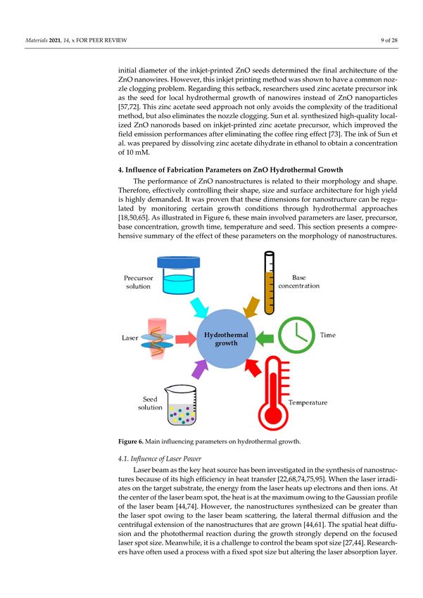
Materials 2021, 14, 4083                                                                                                       2 of 26

                           huge excitation binding energy (60 meV), excellent electron mobility (1 to 200 cm2 /V. s)
                           and huge piezoelectric coefficient (d33 ~12 pm/V) [13,16,17,23,29–31]. Excellent biocompat-
                           ibility, biodegradability and chemical stability, as well as amazing electrical and optical
                           properties are also some great characteristics of ZnO [12,13,15,17,20,25,32,33]. Meanwhile,
                           various morphologies of ZnO nanomaterials have been investigated, such as nanoparticles,
                           nanowires, nanoneedles and nanotubes, which accordingly expand their applications in
                           various fields [12–14,17,19,34].

                           Table 1. Summary of ZnO nanostructure properties.

                                 Type of Property                                        Property
                                                           Easy to grow [12].
                                                           Low- and high-temperature operation capability.
                                    Preparation
                                                           Architecture and property controllability.
                                                           Facility of integration on either rigid or flexible devices [20].
                                                           Large bandgap [13].
                                                           Good transparency to visible light.
                                      Optical
                                                           Luminescent material [20].
                                                           Good transmissibility and reflexibility [35,36].
                                                           Semiconductor material.
                                                           Good electron mobility [37].
                                     Electrical
                                                           Good chemical stability [16].
                                                           Huge piezoelectric coefficient [11,38].
                                                           Excellent biocompatibility [13,20].
                                    Biomedical             Excellent biodegradability [25].
                                                           Non-toxicity [33,37].
                                                           Huge excitation binding energy [16,23].
                                      Energy
                                                           Photocatalytic material [37,39].

                                 ZnO is available in three crystalline structures, including wurtzite, zinc blende and rock
                           salt. Wurtzite structure is a two-lattice parameter-based hexagonal unit cell with a = 0.3296 nm
                           and c = 0.52065 nm [13,18,40]. ZnO wurtzite is stable under ambient conditions, but it is
                           transformed into rock salt at relatively high pressure (approximately 10 GPa) [18,41]. The zinc
                           blende can only be obtained at its stable phase on cubic substrates [20,41].
                                 Various methods have been established to synthesize ZnO nanostructures. These meth-
                           ods can be divided into three groups as follows: (a) wet-chemical synthesis, (b) solid-state
                           synthesis and (c) vapor-phase synthesis [41–43]. Wet chemical synthesis is carried out at low
                           temperatures (
Materials 2021, 14, 4083                                                                                            3 of 26

                           bulk heating [61,68], microcontact printing [17,63,69–71], inkjet printing [17,57,62,72,73] and
                           laser-induced heating [44,46,61,68,74,75] have been developed via the hydrothermal method.
                           These approaches require different setups, processing factors and also different ways for
                           required factors. There are several parameters, such as laser power, seeding of the substrate,
                           the type and concentration of precursor solution, growth duration and temperature, which
                           influence ZnO’s morphology and shape during the growing process. Since properties of ZnO
                           nanostructures are strongly correlated with their morphologies and shapes, it is valuable
                           better to understand these parameters for desired applications [12,21,25]. Furthermore, even
                           though these approaches mentioned above belong to the same family of growth, they possess
                           different advantages and disadvantages.

                           Figure 1. The different synthesis methods of ZnO nanostructures.

                                Recently, comprehensive work was reported in synthesizing ZnO nanostructures for
                           UV sensors [4,40,76]. Their majority was focusing on various synthesis methods. However,
                           each method possesses various approaches and it was short of a detail interpretation about
                           the mechanism of each method. As economic cost for the synthesis is under increasing
                           challenge, a comprehensive review on each method is of great importance for the future
                           study. To the best of authors’ knowledge, no previous review has precisely examined all
                           of hydrothermal approaches and summarized the effect of critical parameters on the ZnO
                           synthesis. Therefore, the current review aims on the latest approaches of ZnO hydrothermal
                           growths and the effect of different parameters on its morphology. This paper provides
                           an overview of the recent developments in ZnO nanostructure synthesis for UV sensors,
                           particularly the hydrothermal synthesis. Different hydrothermal approaches are compared,
                           and the critical parameters are discussed in detail. Lastly, the hydrothermal ZnO-based UV
                           sensors for UV light are discussed as well. This review may provide a better comprehension
                           of the current research status for hydrothermal ZnO-based applications.

                           2. ZnO Nanostructures’ Hydrothermal Growth
                           2.1. Different Types of ZnO Nanostructures
                               ZnO is a fascinating material with various morphologies. The chemical and physical
                           characteristics vary as a function of morphology, size, shape and crystalline structures.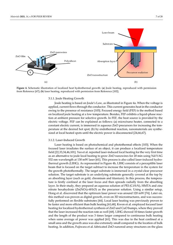
Materials 2021, 14, 4083 4 of 26
Previous works have demonstrated that this material can be modelled on the desired shape
and size [12,14,17,18,42,77].
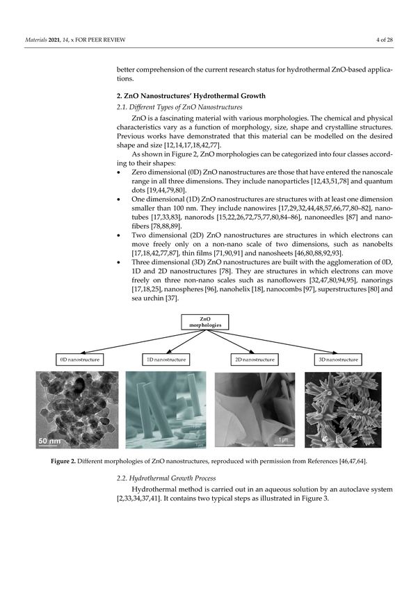
As shown in Figure 2, ZnO morphologies can be categorized into four classes accord-
ing to their shapes:
• Zero dimensional (0D) ZnO nanostructures are those that have entered the nanoscale
range in all three dimensions. They include nanoparticles [12,43,51,78] and quantum
dots [19,44,79,80].
• One dimensional (1D) ZnO nanostructures are structures with at least one dimen-
sion smaller than 100 nm. They include nanowires [17,29,32,44,48,57,66,77,80–82],
nanotubes [17,33,83], nanorods [15,22,26,72,75,77,80,84–86], nanoneedles [87] and
nanofibers [78,88,89].
• Two dimensional (2D) ZnO nanostructures are structures in which electrons can move
freely only on a non-nano scale of two dimensions, such as nanobelts [17,18,42,77,87],
thin films [71,90,91] and nanosheets [46,80,88,92,93].
• Three dimensional (3D) ZnO nanostructures are built with the agglomeration of
0D, 1D and 2D nanostructures [78]. They are structures in which electrons can
move freely on three non-nano scales such as nanoflowers [32,47,80,94,95], nanor-
ings [17,18,25], nanospheres [96], nanohelix [18], nanocombs [97], superstructures [80]
and sea urchin [37].
Figure 2. Different morphologies of ZnO nanostructures, reproduced with permission from References [46,47,64].
2.2. Hydrothermal Growth Process
Hydrothermal method is carried out in an aqueous solution by an autoclave sys-
tem [2,33,34,37,41]. It contains two typical steps as illustrated in Figure 3.
• Seeding: The subtract is seeded with a layer of ZnO nanoparticles. The seeded
nanoparticles play a role in promoting nucleation for nanostructure growth by de-
creasing the thermodynamic barrier. The less the nucleation of ZnO is, the bigger ZnO
growth and the better the crystallinity of ZnO [98].
• Growing: The seeded subtract is kept in the precursor at a certain temperature for a
fixed period to ensure stable growing regimes. The precursor is a mixture of aqueous
solutions containing alkaline reagent (such as NaOH, KOH and hexamethylenete-
tramine (HMTA)) and zinc ion salt (such as Zn (NO3 )2 and ZnCl2 ) [39,40,47,99]. In
addition to the precursor, a guiding agent (such as polyethyleneimine (PEI)) is inserted
to decrease the lateral growth and maximize the length of nanostructures.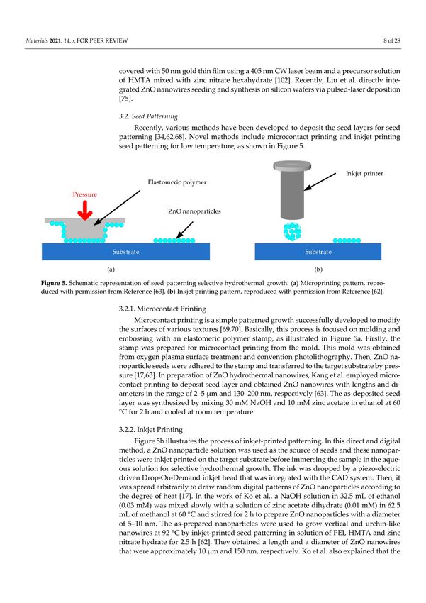
Materials 2021, 14, 4083                                                                                                    5 of 26

                       Figure 3. Diagram of hydrothermal process, reproduced with permission from Reference [2].

                                        Deng et al. employed the hydrothermal process to grow ZnO nanorods on flexible
                                   Kapton substrate at low temperature with an equimolar solution of HMTA and zinc nitrate
                                   hexahydrate as a precursor [19]. They obtained nanorods in the form of regular hexagonal
                                   prisms with a length of 60 nm and a diameter of 100 nm. Vijayakumar et al. presented
                                   ZnO nanotubes synthesized by hydrothermal method in autoclave for 4 h at 90 ◦ C for CO
                                   gas sensing [83]. Hu et al. hydrothermally synthesized ZnO nanowires on polyethylene
                                   terephthalate (PET) fabrics at 95 ◦ C for 4 h [34]. The as-grown nanowires were treated
                                   hydrophobically by polydimethylsiloxane (PDMS) for lotus effect. Via hydrothermal
                                   growth, Wu et al. demonstrated the synthesis of graphene quantum dot doped ZnO
                                   superstructures for weak UV intensity sensor application at 90 ◦ C for 2 h [80].
                                        Typically, the hydrothermal method consists of a series of four chemical reactions. The
                                   chemistry reactions were discussed by Young et al. [40]. Firstly, HMTA was often used
                                   as a precursor and hydrolyzed to the OH- and ammonia. Secondly, OH- ions with Zn2+
                                   ions form a complex of hydroxide of zinc Zn(OH)2 . After then, the Zn(OH)2 was thermally
                                   decomposed into ZnO. These reactions are as follows [33,37,39–41,45,75]:

                                                                C6 H12 N4 +H2 O → 6HCHO + 4NH3                                 (1)

                                                                    NH3 +H2 O → NH4+ +OH−                                      (2)

                                                                     2OH− +Zn2+ → Zn(OH)2                                      (3)
                                                                     2Zn(OH)2 → ZnO + H2 0                                     (4)
                                        In order to control the morphology, orientation, aspect ratio and surface density of the
                                   ZnO nanostructure, parameters involved in the process must be optimized. Examples of
                                   parameters affecting nanostructure growth morphology are the pH of the solution, reagents,
                                   seed layers, temperature, guiding agents, growth time and mechanical agitations [18,50].
                                        Over decades, the hydrothermal technique has proven beneficial for the synthesis of
                                   ZnO nanostructures on either rigid or flexible substrates. Rigid substrates are often con-
                                   cerned about glass [2,22,33,44,48,59,61], whereas flexible substrates include silicon [45,100],
                                   polyimide (PI) [44,45,48,100], PET [19,34,68], polycarbonate (PC) [48,100], Kapton [101],
                                   PDMS [17], carbon fiber [17,29] and paper [17].

                                   3. ZnO Selective Hydrothermal Growth
                                        Recent hydrothermal growths have been developed to synthesize ZnO nanostructures
                                   directly at a localized area on the substrate. These methods are called selective hydrothermal
                                   growth and were categorized into two groups: localized heat and seed patterning. Table 2
                                   summarizes the advantages and disadvantages of these selective hydrothermal growths.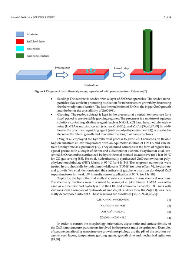
Materials 2021, 14, 4083                                                                                                                         6 of 26

                                   Table 2. Advantages and disadvantages of selective hydrothermal growths.

  Group of           Type of
  Selective         Selective                               Advantages                                           Disadvantages
  Growth            Growth
                                     •      Simple for fabrication [24].
                      Joule          •      Low temperature and single step.                    •   Difficult to apply for 3D complex system [44].
  Localized
    heat          heat-induced       •      Less usage of energy and chemicals.                 •   Problem of leakage current.
                    growth           •      Strong mechanical and electrical contact between    •   Failure at electrical contacts.
                                            the nanomaterials and the devices.
                                     •      Simple and rapid [44,61].
                      Laser-         •      Low temperature, maskless and fully digital.        •   Limited smallest local growth spot size to
                    induced          •      Well-defined configurations.                            several microns [66,68].
                     growth          •      High packing density and possibility of 3D          •   Difficulty of laser power control [44].
                                            structures growth [61,66].
                                     •      Low temperature [63].
                                                                                                •   Fabrication of mold [44].
     Seed         Microcontact       •      Simple.
  patterning       printing                                                                     •   Impossibility of modification of the mold once
                                     •      Freedom of substrate choice.
                                                                                                    fabrication is complete [62].
                                     •      Controllability of geometry.
                                     •      Fast, maskless and digital [62].
                                     •      Low temperature and environmental benign process.   •   Extra step required [44,63].
                 Inkjet printing     •      Freedom of substrate.                               •   Inkjet nozzle clogging problem [72].
                                     •      Scale up for mass production.                       •   Limited ink choice in concentration and viscosity.
                                     •      Ease modification of the growth location due to a
                                            CAD system.

                                         3.1. Localized Heat
                                              In the past decade, two main approaches of localized heat have been established for
                                         selective hydrothermal growth. These approaches include Joule heating and laser heating,
                                         as shown in Figure 4.

      Figure 4. Schematic illustration of localized heat hydrothermal growth: (a) Joule heating, reproduced with permission from
      Reference [67]; (b) laser heating, reproduced with permission from Reference [102].

                                         3.1.1. Joule Heating Growth
                                              Joule heating is based on Joule’s Law, as illustrated in Figure 4a. When the voltage is
                                         applied, current flows through the conductor. This current generates heat in the conductor
                                         owing to the presence of resistance [103]. Focused energy field (FEF) is the method based on
                                         localized joule heating at a low temperature. Besides, FEF exhibits a liquid-phase reaction
                                         at ambient pressure for selective growth. In FEF, the heat source is provided by the electric
                                         voltage. FEF can be explained as follows: (a) micro/nano heater, connected to a constant
                                         electric current, is immersed in aqueous ZnO precursors for increasing the temperature at
                                         the desired hot spot; (b) by endothermal reaction, nanomaterials are synthesized at local
                                         heated spots until the electric power is disconnected [24,66,67].
Materials 2021, 14, 4083 7 of 26
3.1.2. Laser-Induced Growth
Laser heating is based on photochemical and photothermal effects [103]. When the
focused laser irradiates the surface of an object, it can produce a localized temperature
field [22,33,34,46,101]. Yeo et al. reported laser-induced local heating for the very first
time as an alternative to joule local heating to grow ZnO nanowires for 20 min using
Nd:YAG 532 nm wavelength at 130 mW laser [61]. This process is also called laser-induced
hydrothermal growth (LIHG). As represented in Figure 4b, LIHG consists of a perceptible
laser beam that is focused on the target subtract to increase the temperature in the system
for the growth photothermally. The target substrate is immersed in a crystal-clear precursor
solution. The target substrate is an underlying substrate generally covered at the top by an
absorbing layer (such as gold, chromium and titanium). In this process, the temperature is
firstly confined at the laser focus and then spreads radially from the absorbing layer. In
their study, they prepared an aqueous solution of PEI (C2 H5 N), HMTA and zinc nitrate
hexahydrate (Zn(NO3 )2 ·6H2 O) as the precursor solution. Using a similar setup, Hong et al.
discovered that the optimum laser power was around 120 mW [74]. Later on, this method
was proven as digital growth, even on 3D microstructures, and was successfully performed
on flexible substrates [44]. Local laser heating was previously proven to be faster and
more efficient than bulk heating [61,68]. Kwon et al. employed focused laser heating for
localized hydrothermal synthesis of ZnO and CuO bumps, where they proved that the
laser increased the reaction rate as well [68]. LIHG showed 10 times faster growth and
the length of the product was 3 times larger compared to continuous bulk heating when
same average of power was applied [61]. This was due to the heat confined at a small area
and the growth area was also extremely small compared to the location of bulk heating. In
addition, Fujiwara et al. fabricated ZnO nanorod array structures on the glass covered with
50 nm gold thin film using a 405 nm CW laser beam and a precursor solution of HMTA
mixed with zinc nitrate hexahydrate [102]. Recently, Liu et al. directly integrated ZnO
nanowires seeding and synthesis on silicon wafers via pulsed-laser deposition [75].
3.2. Seed Patterning
Recently, various methods have been developed to deposit the seed layers for seed
patterning [34,62,68]. Novel methods include microcontact printing and inkjet printing
seed patterning for low temperature, as shown in Figure 5.
Figure 5. Schematic representation of seed patterning selective hydrothermal growth. (a) Microprinting pattern, reproduced
with permission from Reference [63]. (b) Inkjet printing pattern, reproduced with permission from Reference [62].
3.2.1. Microcontact Printing
Microcontact printing is a simple patterned growth successfully developed to modify the
surfaces of various textures [69,70]. Basically, this process is focused on molding and embossing
with an elastomeric polymer stamp, as illustrated in Figure 5a. Firstly, the stamp was prepared
for microcontact printing from the mold. This mold was obtained from oxygen plasma surface
treatment and convention photolithography. Then, ZnO nanoparticle seeds were adhered to
the stamp and transferred to the target substrate by pressure [17,63]. In preparation of ZnOMaterials 2021, 14, 4083 8 of 26
hydrothermal nanowires, Kang et al. employed microcontact printing to deposit seed layer and
obtained ZnO nanowires with lengths and diameters in the range of 2–5 µm and 130–200 nm,
respectively [63]. The as-deposited seed layer was synthesized by mixing 30 mM NaOH and
10 mM zinc acetate in ethanol at 60 ◦ C for 2 h and cooled at room temperature.
3.2.2. Inkjet Printing
Figure 5b illustrates the process of inkjet-printed patterning. In this direct and digital
method, a ZnO nanoparticle solution was used as the source of seeds and these nanoparti-
cles were inkjet printed on the target substrate before immersing the sample in the aqueous
solution for selective hydrothermal growth. The ink was dropped by a piezo-electric
driven Drop-On-Demand inkjet head that was integrated with the CAD system. Then, it
was spread arbitrarily to draw random digital patterns of ZnO nanoparticles according
to the degree of heat [17]. In the work of Ko et al., a NaOH solution in 32.5 mL of ethanol
(0.03 mM) was mixed slowly with a solution of zinc acetate dihydrate (0.01 mM) in 62.5 mL
of methanol at 60 ◦ C and stirred for 2 h to prepare ZnO nanoparticles with a diameter
of 5–10 nm. The as-prepared nanoparticles were used to grow vertical and urchin-like
nanowires at 92 ◦ C by inkjet-printed seed patterning in solution of PEI, HMTA and zinc
nitrate hydrate for 2.5 h [62]. They obtained a length and a diameter of ZnO nanowires that
were approximately 10 µm and 150 nm, respectively. Ko et al. also explained that the initial
diameter of the inkjet-printed ZnO seeds determined the final architecture of the ZnO
nanowires. However, this inkjet printing method was shown to have a common nozzle
clogging problem. Regarding this setback, researchers used zinc acetate precursor ink as
the seed for local hydrothermal growth of nanowires instead of ZnO nanoparticles [57,72].
This zinc acetate seed approach not only avoids the complexity of the traditional method,
but also eliminates the nozzle clogging. Sun et al. synthesized high-quality localized ZnO
nanorods based on inkjet-printed zinc acetate precursor, which improved the field emission
performances after eliminating the coffee ring effect [73]. The ink of Sun et al. was prepared
by dissolving zinc acetate dihydrate in ethanol to obtain a concentration of 10 mM.
4. Influence of Fabrication Parameters on ZnO Hydrothermal Growth
The performance of ZnO nanostructures is related to their morphology and shape.
Therefore, effectively controlling their shape, size and surface architecture for high yield is
highly demanded. It was proven that these dimensions for nanostructure can be regulated
by monitoring certain growth conditions through hydrothermal approaches [18,50,65]. As
illustrated in Figure 6, these main involved parameters are laser, precursor, base concentra-
tion, growth time, temperature and seed. This section presents a comprehensive summary
of the effect of these parameters on the morphology of nanostructures.
Figure 6. Main influencing parameters on hydrothermal growth.Materials 2021, 14, 4083 9 of 26
4.1. Influence of Laser Power
Laser beam as the key heat source has been investigated in the synthesis of nanos-
tructures because of its high efficiency in heat transfer [22,68,74,75,95]. When the laser
irradiates on the target substrate, the energy from the laser heats up electrons and then ions.
At the center of the laser beam spot, the heat is at the maximum owing to the Gaussian
profile of the laser beam [44,74]. However, the nanostructures synthesized can be greater
than the laser spot owing to the laser beam scattering, the lateral thermal diffusion and the
centrifugal extension of the nanostructures that are grown [44,61]. The spatial heat diffu-
sion and the photothermal reaction during the growth strongly depend on the focused laser
spot size. Meanwhile, it is a challenge to control the beam spot size [27,44]. Researchers
have often used a process with a fixed spot size but altering the laser absorption layer. As a
result, the laser-induced temperature was regulated via changing the thermal conductivity
or the physical dimension (such as thickness and diameter) of the absorbing layer [44].
The laser plays three significant roles in hydrothermal growth. Firstly, the direction of
the laser beam towards the target substrate is crucial. Two laser beam irradiation configu-
rations are possible. The laser beam is either focused from the top on the same side of the
subtract (Figure 7) or from the bottom (Figure 4b). Yeo et al. proved that higher quality
of ZnO nanowires was obtained when the laser beam irradiation was on the opposite
side to the growth due to a low induced temperature [61]. Fujiwara et al. also employed
a similar irradiation direction to optimize the random lasing properties [102]. However,
Yeo et al. successfully synthesized digital ZnO nanowires with a greater dimension than
that of the laser spot directly on the growth side [44]. Liu et al. also used top focusing of
the laser for the successful nucleation of ZnO nanoparticles and ZnO nanowire growth [75].
Even so, the bottom focusing case is more efficient, stable and preferable because there
is no direct interaction between the nanostructures and the laser beam [61]. Secondly,
it is because of the laser intensity. A higher intensity increases the growth rate because
more photons are absorbed and then a higher temperature is generated. Fujiwara et al.
discovered that the quality of ZnO nanorods was improved with an increase of the ex-
citation laser intensity [102]. The higher value of the laser intensity made an increase in
ZnO film quality and a decrease in sheet strength [32]. However, there was a maximum
laser intensity and its excess destroyed the synthesized nanostructures [29,32,61]. Third,
laser power is associated with the diameter of the laser as well. Jung et al. conducted
two growth experiments to show that the laser power and beam diameter significantly
influence the nanostructure morphology [104]. It was found that the laser beam with the
smaller diameter produced ZnO faster and longer owing to higher laser energy at the spot
center. Results showed that the growth output is proportional to laser power due to the
increase of induced temperature, which plays a role of a catalyst in the chemical reactions.
Furthermore, there is a minimum laser power for nanostructure growth to occur.
Figure 7. Top focusing method of laser-induced hydrothermal growth, reproduced with permission
from Reference [44].Materials 2021, 14, 4083 10 of 26
4.2. Influence of Precursor Solution
The mixture of precursor solution is mainly responsible for the chemical reaction
during hydrothermal process. The careful control of initial reaction and precursor condi-
tions gave predicted stoichiometric compositions of final arrivals. Multiple metal oxide
nanostructures can be directly grown on the same substrate with consecutive hydrothermal
growths with different precursor mixtures [1,2,44]. For instance, Yeo et al. applied LIHG
twice with separate precursors to synthesize ZnO and TiO2 nanowires on the same PI
substrate [44]. As mentioned in Table 3, precursors play an important role on the size of
the nanostructures.
Table 3. Advantages and disadvantages of selective hydrothermal growths.
ZnO Synthesis Growth Diameter of ZnO Length of ZnO
Starting Materials References
Morphology Temperature (◦ C) Time Nanostructures Nanostructures
25 mM of zinc nitrate hexahydrate,
Nanowires 95 1h 200–400 nm 10–12 µm [61]
25 mM HMTA and 5–7 mM PEI.
25 mM of zinc nitrate hexahydrate,
Nanowires 25 mM HMTA, 5–7 mM PEI and 95 1h >20 µm - [44]
deionized (DI) water.
25 mM of zinc nitrate hexahydrate,
Nanowires - - - 9.9 µm [24]
25 mM HMTA and 6 mM PEI.
25 mM of zinc nitrate hexahydrate,
Nanowires 90 2.5 h 100–150 nm 1–3 µm [72]
25 mM HMTA and 5–7 mM PEI.
25 mM of zinc nitrate hexahydrate,
Nanowires 95 1h 15 µm 200–400 nm [105]
25 mM HMTA and 5–7 mM PEI.
Hemispherical Mixture of equimolar zinc nitrate
90 5h 400 nm 2.2 µm [64]
bumps hexahydrate and HMTA.
Mixture of equimolar zinc nitrate
Nanorods 90 3h 100 nm 800 nm [106]
hexahydrate and HMTA.
50 mL of solution containing
Nanorods 0.1 M zinc nitrate hexahydrate, 90 2h 70 nm 15 µm [26]
0.1 M HMTA and DI water.
Mixture of equimolar zinc nitrate
Nanorods 90 4h 1.2 - [2]
hexahydrate and HMTA
Flower-like Zinc acetate dehydrate and NaOH. 120 15 min 0.6 µm 5.2 µm [32]
structure
Nanowires ZnCl2 . NaCO3 and DI water. 140 6h 50 nm 1 µm [65]
Vertical
aligned Zn(CH3 COO)2 ·2H2 O, HMTA, absolute 400 - 50 nm 500 nm [13]
ethanol and distilled water.
nanorods
10 mL Zn(Ac)2 .2H2 O in 0.1 M methanol,
20 mL NaOH in 0.5 M methanol, 150 2.8 nm 26 nm
DI water (K2 SnO3 ,3H2 O, 95%), 24 h
0.75 g of urea.
Nanorods [42]
90 ◦ C for 100 min,
dried for 12 h
20 mM Zn(NO3 )2 and 20 mM HMTA at 60 ◦ C and - 290–330 nm 3.2–3.4 µm
annealed 1 h
at 500◦ C.
-: Not reported.
The change of the precursors significantly influences the output results [65,78,98].
Naif et al. investigated the effect by altering zinc acetate dehydrate, zinc nitrate hexahydrate
and zinc chloride [65]. Their finding was that the zinc salt precursors significantly influence
the aspect ratio and the morphology of nanowires.
Adequate control over the chemical reactants was utilized to regulate morphologies
and the size of the final ZnO-grown nanostructures [31,32,64,78,106]. By varying the
concentration of the reactants from 0 to 400 mM, Amin et al. demonstrated that the length,
diameter and density of the ZnO nano/micro rods were also varied [64]. According to
their findings, nano/microrod, wire-like rods and ultrathin nanowires can be obtained by
adjusting the precursor concentration. There is limit for only the radial growth when the
concentration is continuously increased. The rods became thin film at higher concentration.Materials 2021, 14, 4083 11 of 26
Additionally, Yeasmin et al. proved that nanorods synthesized under low precursor
molarity resulted in thinner rods [31].
The pH value of the precursor mixture has an important influence on the output
products for the growth of nanomaterials with chemical route [39,64,65,89,104]. When the
pH increased by adding ammonium, ammonia hydrolyzed into NH4+ through Equation (2)
and Zn(OH)2 rose according to the increase of OH- concentration in the solution described
by Equation (3). When the pH was decreased by adding HCl or HNO3 (pH < 7), the disso-
lution of the precipitates occurred through Equation (3) followed by the rise of formation
of Zn2+ ions leading to larger and longer nanorods. According to Amin et al.’s work,
morphologies and sizes were varied with the pH and there was a critical pH value where
there was etch instead of growth [64]. Figure 8 shows the variation of ZnO morphologies
with different pH of the precursor solution. ZnO nanorods were obtained at pH = 6.6,
nanotetrapod ZnO was obtained at pH = 8, flower-like structures were obtained at pH = 9.1,
urchin-like structures at pH = 11.2, no growth at pH < 1.8 and ultralong and ultra-large
nanorods at a pH between 1.8 and 4.6 [64]. Young et al. also synthesized nanowires,
nanostars and nanoflowers at pH = 6.53, 8.18 and 9.18, respectively [107].
Figure 8. ZnO morphology versus pH of precursor.
4.3. Influence of Base Concentration
To get desired nanostructure morphologies, base solutions such as NH4 , NaOH and
KOH were added to the growth solution [17,18,20,41,99]. It was proved that a supersat-
urated solution in Na2 CO3 was a significant factor for the synthesis of nanowires due to
its action as a weak base hydrolyser in the water solution and producer of OH [77]. Naif
et al. experimented with the base concentration of 2.044 M, 2.673 M, 3.145 M, 4.193 M
and 4.717 M to scale up the fabrication of nanowires [65]. According to their findings, the
synthesis of nanowires was started when the base was above the saturation concentration
of Na2 CO3 (in their case, the saturation level was 2.673 M). They also found that an increase
of Na2 CO3 concentration caused the enhancement in the length of ZnO nanowires, but
a decrease in diameter because higher Na2 CO3 concentration resulted in the side facets
becoming positively charged and suppressing lateral growth. Altering the concentration
of base solutions in the aqueous solution resulted in ZnO nanostructures with different
properties [16,89]. Lu et al. hydrothermally achieved the growth of ultralong nanobelts
with honey-like micropattern on the Zn foil at 150 ◦ C with concentrations of NaOH and
(NH4 )2 S2 O8 of 2 M and 0.4 M, respectively [108].
With cautious adding ammonium hydroxide NH4 OH in the precursor mixture, Boube-
nia et al. discovered a possibility of enhancing the nucleation sites, which led to the control
of nanowires’ electrical properties and expanded the applications for flexible and elec-
tromechanical devices [16]. Based on their work, they explained the density-controlled
synthesis growth mechanism of ZnO nanowires as follows: The amount of NH4 OH had
a straight effect over the concentration of Zn (II) complexes, which would significantly
impact the Zn solubility in the solution. Thus, the supersaturation of precursor solution
was controlled as well as the quantity of nuclei over the target substrate.Materials 2021, 14, 4083 12 of 26
4.4. Influence of Growth Time
In hydrothermal growth process, growth time is another important critical parameter
of ZnO nanostructures [48,65,87,97,99]. As shown in Table 3, researchers fabricated ZnO
nanostructures with different growth times to set up the relationship between yield of
growth and their morphologies.
In laser-induced growth, nanorods’ diameter became larger and their density became
less with the increase of growth time, but the nanorod lengths were almost unchanged with
the growth time [22,102]. Control over the growth time enabled only an optimization of the
radial growth of ZnO nanowires, as indicated in Figure 9a [44,61,74]. This phenomenon is
due to the nucleation and growth theory, where rather than forming new nanostructures,
ZnO was successively deposited on the preformed ZnO nanostructures. Initially, it was
the absorbing layer that heated the precursor solution. At a certain level of the precursor
solution’s temperature, the continuous formed ZnO components were oversaturated and
resulted in a trigger of the nucleation process. Then, the ZnO nanostructures were nucleated
and the growth on the hot area of the absorbing layer was taken place. Once the nucleation
began, the growth of ZnO nanostructures consumed the ZnO component in the precursor
solution and this avoided further oversaturation of ZnO components. Thus, it became
impossible to form new ZnO nanostructures nuclei to enhance the packaging density [22].
Figure 9. ZnO nanowires synthesized by hydrothermal method at different growth time. (a) SEM images of diameter, repro-
duced with permission from Reference [44]; (b) SEM images of length, reproduced with permission from Reference [100];
and (c) length and diameter versus growth time, reproduced with permission from Reference [65].
The growth time monitors the aspect ratio of ZnO morphology. In hydrothermal
growth, the length of nanorods was continuously and steadily increased with the increase
of time, as shown in Figure 9b [64,65,100]. Above a specific time, there was no further
expansion of the length due to a closure–precipitation equilibrium. Amin et al. attributed
this observation to the fact that at a certain time, the OH- was consumed due to the
hydrolyze of OH- in water from HMTA, leading to the termination of the reaction [64].
Naif et al. successfully synthesized ZnO at different growth times from 3 to 26 h in the
following conditions: 140 ◦ C with 4.193 M Na2 CO3 and 0.032 M ZnCl2 . As shown in
Figure 9c, the results firstly emphasized that the length of ZnO nanowires increased fromMaterials 2021, 14, 4083 13 of 26
1.1 to 3.3 µm with a prolonged growth time due to an Ostwald ripening process, while
the diameter was kept constant around 41 nm. Secondly, the length of ZnO was almost
constant from 16 h since Zn2+ ions were consumed in the mixture [65]. By further increasing
the time, ZnO nanorods continually grew longer along the (001) direction and became
wider along the (010) direction, whereas, with higher growth durations, the diameter
decreased [106,108]. These results pointed out that the ZnO nanostructures grew only
along the c-axis after the initial nucleation. The mechanism responsible for this exclusive
axial growth may be the alkaline condition of the precursor solution. This mechanism was
due to track ions such as acetate ions and/or carbonate ions. In fact, when the precursor
solution was alkaline, the (1120) side facets and the (0001) end facets of ZnO nanowires
became positively and negatively charged, respectively. This in turn suppressed the radial
growth [65].
4.5. Influence of Growth Temperature
The hydrothermal method occurs at low temperatures and in an autoclave environ-
ment. Therefore, the temperature also has a significant role in controlling the structure
morphology. Table 3 mentioned the effect of temperature on the geometry of ZnO.
The role of the temperature is to heat the mixture of precursors in autoclave to activate
the chemical reactions. For example, the growth reaction was accelerated at higher tempera-
tures because an increase of OH– ion concentration was caused by the faster decomposition
of HMTA at higher temperatures [104]. The range of appropriate temperature growth
depended on the different semiconductor materials. For instance, the range of proper
temperature for TiO2 nanowires (120–180 ◦ C) was higher than for that of ZnO nanowires
(60–120 ◦ C) [44].
The temperature was found to control the size of ZnO nanostructures [64,65,73,78].
To investigate the influence of the temperature on ZnO nanowires, Amin et al. conducted
a hydrothermal growth of nanorods in aqueous solution with a constant pH (pH = 6.6),
specific growth time (t = 5 h) and a fixed precursor concentration (100 mM), and the
growth temperature was changed from 50 ◦ C to 110 ◦ C [64]. Their results indicated that
the ZnO nanorods’ aspect ratio increased with the temperature up to 95 ◦ C but no further
enhancement was found in the aspect ratio above 110 ◦ C. Through their findings, they
affirmed that the feasible temperature for growth was less than 100 ◦ C. There was an
optimum temperature where a high density of ZnO nanowires grew in a uniform and
conform fashion [100]. Naif et al. carried out similar work at higher temperatures (at
120 ◦ C, 140 ◦ C and 160 ◦ C) and discovered that the high yield of growth was centered
around 140 ◦ C (diameter and length are 50 nm and 1 µm, respectively) [65].
The type of synthesized ZnO nanostructures is also affected by the temperature. On
the Zn foil substrate, Lu et al. synthesized well-aligned ZnO nanorods of 30 nm in diameter
and 200 nm in length at 22 ◦ C and ultralong ZnO nanowires arrays with honeycomb-like
structures of 60 to 200 nm in diameter and 10 to 30 mm in length at elevated temperature
under similar conditions [108].
In hydrothermal method, ZnO nanostructures were treated with thermal annealing af-
ter either the seed deposition or the growth in order to alter their properties [1,106,109,110].
For instance, Filip et al. reported a significant difference in crystalline structure on a seed
layer between annealed and non-annealed substrates [35]. Lupan et al. demonstrated that
post-treatment thermal annealing led to improvement in the crystallinity and the perfor-
mance of ZnO nanomaterials [82]. Sandeep Sanjeev and Dhananjaya Kekuda also showed
that annealing temperature affected the structural and optical properties of the ZnO thin
film [36]. Wahid et al. reported that the optimum annealing temperature was 150 ◦ C, where
they obtained high-resistant ZnO nanorods with a length and diameter of 4000 nm and
379 nm, respectively [86]. They also discovered that the ZnO growth rate depended on
the annealing temperature, as vertical nanorods were observed below 150 ◦ C and ZnO
homocentric bundles on the vertical nanorods above 150 ◦ C. Through careful analysis of
the seed layer, Wahid et al. explained the mechanism behind this observation as follows.Materials 2021, 14, 4083 14 of 26
At annealing temperatures above 150 ◦ C, more energy was present in the seed layer, which
enhanced the kinetic energy of the seed layer molecule. In consequence, the molecular mo-
tion increased and this caused the seed layer to stretch more and reduce the surface tension.
As a result, the seed nanoparticles agglomerated, which then brought the nanoparticles
together during the annealing process. As the seed nanoparticles were agglomerating,
the active nucleation sites of ZnO seed were disorientated, resulting in multifarious ZnO
nanorod growth orientation, which promoted bundling of the ZnO nanorods [86,111].
Meanwhile, Wei et al. reported that this agglomeration phenomenon happened because
annealing produced the dried organic compound (diethanolamine) [112].
4.6. Influence of the Seed Solution
The seed layer condition and coating are critical for high-yield ZnO nanostructures’
growth from the initial crystal nucleation [17,100]. ZnO nanowires and nanorods were
unsuccessfully grown without seed coating [95,100]. Asib et al. discovered that bigger and
less distributed ZnO nanorods were synthesized on glass without a seed layer compared
to a compact and denser distribution of thin ZnO nanorods synthesized on glass with a
TiO2 layer because the glass did not provide the nucleation for nanostructures to grow [2].
Yoo et al. hydrothermally synthesized a conform and uniform large area of ZnO nanowires
using ZnO nanoparticle seeds and Ag seeds [100]. They explained that the Ag-seeded
substrate needed a longer time and higher temperature (130 ◦ C) compared to the ZnO-
seeded substrate for the same length.
In the work of Farhad et al., they revealed that pre-depositing ZnO seed layer was
beneficial for synthesizing aligned ZnO nanorods along the c-axis direction parallel to the
substrate due to the high relaxation [95]. They also showed that the optical characteristics,
such as reflection and transmission of ZnO nanorods, were enhanced. Still, the optical
bandgap stayed unchanged when nanorods were prepared on seeded soda line glass
(SLG) and fluorinated tin oxide (FTO) compared to those prepared on a non-seeded layer.
The reason was that the pre-deposition of the ZnO seed layer promoted thicker and
denser ZnO nanostructures. In the same perspective, Filip et al. also demonstrated the
similar impact of seed treatment on the structures, morphology and optical properties
using a one-step hydrothermal process [35]. Their results showed a successful synthesis
of ZnO nanorods and nanoplates with homogeneous configuration on seeded glasses
with three different seeded layers (zinc acetate, ethanolamine and 2-methoxyethanol).
Filip et al.’s nanostructures provided excellent antireflection properties with an enhancing
of transmittance up to 90% and a reduction of the bandgap energy to 3.22 eV.
Lower concentrations of seed solution result in better crystallinity of ZnO. Eom et al.
reported that the shape of the ZnO structures changed to nanowires while the crystallinity
was poorer and the size of the crystalline was smaller when the seed solution to growth
solution (S/G) ratio was increased. Nanorods with the best crystallinity and wurtzite
structure were successfully achieved with S/G = 1:10 [98].
5. ZnO-Based UV Sensors
UV sensors have great applications, including flame detection, UV communication, UV
calibration and monitoring, missile tracking, astronomical science, industrial production
and healthcare, as classified in Figure 10 [3,4,17,19]. Therefore, a strong and high demand
for the excellent performance, high stability and a simpler fabrication process in UV detec-
tion systems is increasing. This requires excellent photoresponsivity in the UV wavelength
bands [19]. Based on the working principle of UV sensors, ZnO-based UV detectors can be
summarized in five types, including photoconductive, metal-semiconductor-metal (MSM),
Schottky barrier, p-n and p-i-n junctions [4,5]. Zou et al. detailed the explanation of the
mechanism, and the advantages and the disadvantages of each type [4].Materials 2021, 14, 4083 15 of 26
Figure 10. Application of UV sensors (military, medical, industrial and other applications).
The properties of ZnO, including piezo-phototronics and piezotronics, are of great
interest for the realization of UV sensors [38,60,113,114]. The piezo-phototronic effect of
ZnO boosted ZnO-based UV sensors through coupling photons with semiconducting,
optical and piezoelectric properties in the material [81,115]. Particularly, the strain/stress-
induced piezoelectric polarization charges may tune one or more of the procedures during
the photon–semiconductor interaction, such as photon-excited carrier creation, separa-
tion, transport and recombination at the p–n junction and metal-semiconductor (M–S)
contact [10,93]. Besides, the piezo-phototronic effect may provide tunable optoelectronics
by using piezoelectric polarization charges as the gate bias to regulate the interface of the
Schottky barrier or electronic energy states. On the other hand, piezotronics couples the
semiconducting and piezoelectric properties of ZnO through stress/strain [11,38,113]. The
polarity and magnitude of the piezoelectric potential within ZnO depend on the polar
direction of the crystal as well as the magnitude and direction of the mechanical actuation.
The generated piezoelectric potential can tune the Schottky barrier at the M–S interface by
altering the redistribution of free carriers during the contact [93]. Recently, Boruah clarified
the plasmonic, piezo-phototropic and phototropic effects of ZnO for the optimization of the
performance of UV photodetectors (PDs) [76]. He also classified UV PDs in two categories:
conventional and self-powered UV PDs. Conventional UV PDs include MSM and the
Schottky junction. Self-powered UV PDs include the Schottky junction, p-n junction and
photoelectrochemical cells.
In this work, all the above-mentioned sensors are classified on the basis of the compo-
sition of ZnO nanostructures. This classification consists of two groups, including pure
ZnO nanostructures and ZnO composites. In this section, we elaborate on full insight into
ZnO UV applications.
5.1. Pure ZnO Nanostructures for UV Sensing
It is known that the conductivity of ZnO nanostructures changes when they are
exposed to UV light [61,72,74,88]. Numerous works reported that two ZnO nanostructures
arrays connected as a bridge network could be used for MSM UV detection during the lastMaterials 2021, 14, 4083 16 of 26
decade, as shown in Figure 11a [20,24,72]. The longer the nanostructures were, the better
they were connected [61]. Consequently, the sensitivity of the device increased. For instance,
Yeo et al. demonstrated the applicability of ZnO nanowires on 3D structures for use in
MSM PDs [61]. The current of Yeo et al.’s sensor with the UV light was approximately 11 nA
under 1 V external bias. Kwon et al. designed a similar UV sensor using ZnO hemispherical
bumps, but with the photocurrent of 100 nA at a 1 V bias voltage [68]. Table 4 summarizes
the UV sensing property of pure ZnO with different morphologies.
Figure 11. ZnO nanostructure-based UV sensor. (a) Schematic diagram of UV sensor with ZnO nanostructures, bridge
network and (b) sensing mechanism, reproduced with permission from Reference [75].
The principle of the MSM UV sensor is illustrated in Figure 11b. In the dark environ-
ment, the oxygen molecules capture the free electrons to form a depletion region. Under
UV illumination, ZnO absorbs UV light to excite electrons in the valence band to the con-
duction band and generate electron–hole pairs. Amongst these photo-induced hole pairs,
holes are trapped at the oxygen-related hole-trapping states. Generally, these states exist at
the surface of the nanostructure. Since the number of electrons and holes is unbalanced, the
recombination rate decreases. The remained electrons are either re-adsorbed to the oxygen
molecules at the surface, aggregated at the anode or recombined with the ionized hole. The
sensor mechanism is described through the three reactions as follows [23,61,68,74]:
O2(g) +e− → O2−(ad) (5)Materials 2021, 14, 4083 17 of 26
hv → h+ +e− (6)
h +O2−(ad) → O2(g)
+
(7)
For the light with shorter wavelength than the bandgap of ZnO, the photo-generated
holes combine with adsorbed oxygen ions and thereby are detached from the surface of ZnO
nanostructures. Furthermore, the conductivity is also increased by these photo-generated
electrons due to the increase in density of electrical carriers [68,74].
Table 4. Summary of UV sensing properties of pure ZnO nanostructures.
UV Light Photocurrent Dark Current Responsivity Response/Recovery
ZnO Morphology (nm) Iph (A) Idark (A) (A/W) Time (s) References
Nanowires 365 1.1 × 10⁻⁵ 20 Idark - - 20/40 [72]
Nanorods 300–370 - - 2 72/110 [23]
Nanowires - - - - 4.2/4.41 and 29.32/38.86 [74]
Nanorods Sunlight 118 Idark - - 35/46 [106]
Nanorods 365 - - - 50–100/35–40 [98]
Nanorods 365 2.7 × 10⁻³ 2 × 10⁻⁵ 2 × 10⁴ - [26]
Nanorods - 1.98 × 10⁻⁸ 1.97 × 10⁻⁸ 2.22 × 10⁻⁷ 60/- [2]
Nanoflowers 184–365 8× 10⁻⁴ 10−4 92 - [32]
Nanowires - - - 12.4 × 10⁻³ - [110]
Nanowires 365 2.7 × 10⁻⁶ 1.1 × 10⁻⁶ - 1.18/>12.1 [9]
-: Not reported.
By controlling the laser power and growth time, Hong et al. easily integrated ZnO
nanowires into the prefabricated electrode layers to form a photoconductive channel [74].
They used LIHG twice for bridging the gaps between the two electrode pads to demonstrate
a photoconductive UV sensor. Their sensor displayed a significant increase of current by 2
to 3 orders of magnitude when exposed to UV light at a fixed voltage, which showed an
apparent response to UV light. Comparing the performance of sensors with single, double
and triple ZnO nanowires, Hong et al. discovered that the triple junction showed the best
photoresponsivity with rising times of 4.2 s and 29.32 s and decay times are of 4.41 s and
38.6 s, respectively.
Powerful UV devices have also been designed on flexible material through hydrother-
mal methods because of their low temperature. Yang et al. employed FEF-synthesized
nanowires to design ZnO-based devices with outstanding UV and gas sensing as well as
excellent robustness and mechanical loading conditions on a PI substrate [24]. At a 1 V bias,
the current of the designed sensor was significantly enhanced from 240 pA in the dark to
24.1 nA under UV light. Their sensor showed fast responsivity, high sensitivity and good
repeatability. Furthermore, Samoucco et al. fabricated sensors that successfully detected
UV light with a responsivity of 2 and 92 nA/W at a bias of 1 V for PEI and PI substrates,
respectively [32]. They selected and deposited flower-like and rod-like ZnO nanostructures
with a higher surface-to-volume ratio through drop-casting on the electrodes, which, in
turn, were optimized to improve the electrical properties via varying the laser power and
speed. Additionally, their PI sensor proved to operate under strain and be stable after long
hours of operation.
Recently, the excellent control over the concentration of solutions (either seed solution,
precursor solution or both) has significantly resulted in fabrications of higher-quality UV
devices. Nagpal et al. manufactured a cost-effective and non-degradable UV sensor, corre-
sponding to the WHO standard UV sensor [106]. They hydrothermally synthesized ZnO
nanorods on ITO electrodes with varying precursor concentrations and growth durationsMaterials 2021, 14, 4083 18 of 26
for the device. They reported that the sensitivity and the response speed of UV device
decreased with increases in both precursor concentration and growth time. Nanorods
with the best morphology were obtained with from 5 mM concentration and 3 h growth
duration (vertical nanorods and an aspect ratio of 6). Their UV sensor showed a good
response under sunlight with a sensitivity of 118, rise time of 35 s and decay time of 65 s.
Eom et al. studied four different values of S/G (0.1, 4, 10 and 20) to investigate their effect
on the electrical properties and reactivity of UV light sensors [98]. This study discovered
that increasing the molecular concentration of the growth solution allowed them to grow
ZnO in the shape of nanowires rather than nanorods. Moreover, the photocurrent, response
and UV sensitivity of the sensor worsened because the increase of seeds increased the
nucleation site, which limited the growth of ZnO and further degraded the crystallinity of
ZnO. In addition, their study showed that good crystallinity of ZnO nanorods controlled
the high maximum photocurrent and response of UV sensors because they acted well as an
electron transport layer. A UV sensor with a higher photocurrent, higher reactivity and
shorter response time was fabricated with the ratio S/G equal to 1:10.
To design sensors with pure ZnO nanostructures, Qazi et al. prepared ZnO nanorods
at a low temperature (90 ◦ C) on pre-molded seeded substrates by a selective hydrother-
mal method [23]. The as-prepared nanorods formed a bridge between two microspace
electrodes without destroying the electrode interface and geometry. Sensors showed fasci-
nating performances such as low power, fast sensitivity and reproducibility. The designed
sensor was in high gain (3.11) and its sensitivity was 2 A/W at 5 V applied voltage. The
response and recovery times were 72 s and 110 s, respectively.
In order to prove the improvement of UV sensors via heterojunction, scientists fabri-
cated pure ZnO-based UV sensors with an acceptable speed response to UV light [2,9,26,110].
For instance, Liu et al. designed a pure ZnO nanowire-based UV PD on Si substrate with
sensitivity lower than that of a graphene/ZnO one (1.46 compared to 10.71) by growing
nanowires at 120 ◦ C [9]. Noothongkaew et al. also prepared a pure ZnO nanorod that
showed a lower UV response (2 × 10⁴ A/W) to 365 nm UV light compared to CuO/ZnO
composite one (8 × 10⁴ A/W) through their investigation [26].
5.2. ZnO-Based Composites for UV Sensing
Hybrid ZnO with other materials enhanced the sensing property of ZnO-based sen-
sors [12,17,21,33,41,71]. This enhancement is due to two reasons. Firstly, combined ma-
terials form the heterojunction, homojunction and Schottky junction, which reduce the
grain boundaries’ barrier and allow electrons to migrate easily inside the material. Sec-
ondly, there are synergistic effects among the different components of the material com-
posite [4,12,21,116]. These combined materials include hetero-elements (such as Ni, Cu,
Pt . . . etc.), metal oxide (such as CuO, SnO2 and In2 O3 ), carbon materials (such as carbon
nanofiber and carbon nanotube) and two-dimensional materials (such as GaN, SiC and
graphene) [4,7,25,28,79,99,116]. Table 5 summarizes the UV sensing performance of ZnO
composites materials. Here, we discuss ZnO-based composite UV applications.
To fabricate a transparent and flexible UV sensor, Yoo et al. successfully developed
low-temperature Ag-seeded hydrothermal nanowires grown on flexible plastics such
as PET and PC [100]. Under UV light, the role of Ag electrodes was to collect the free
electrons separated from the generated excitons inside the ZnO nanowires, resulting in a
photocurrent signal [85]. The investigation of these UV sensors showed a clear response
to UV power density. They also optimized the sensing performance as well as device
transmittance by adjusting the ZnO nanowires’ Ag structures via the variation of growth
time and temperature [100].
Using a composite detection structure consisting of ZnO nanorods and nanofiber,
Feng et al. reported a simple, efficient and cost-effective UV light detection configuration
with wavelength selectivity [89]. Via their experimental work, they discovered OH− as the
key factor in the hydrothermal growth of ZnO nanorods. When the concentration of OH−
was varied between 0.01 and 0.03 M, ZnO nanorod films with different configurations wereMaterials 2021, 14, 4083 19 of 26
obtained. The OH− concentration of 0.015 M was reported the most appropriate condition
of ZnO nanorod growth and nanorods with higher density, uniformity and higher specific
area were obtained.
Table 5. Summary of UV sensing performance of ZnO composites.
Composite ZnO UV Light Photocurrent Dark Current Sensitivity Responsivity Response/
Recovery References
Materials Morphology (nm) Iph (A) Idark (A) W/(mW cm−2 ) (A/W)
Time (s)
Single-mode
nanorods 365 - - 7.096 - - [89]
fiber/ZnO
Si/ZnO nanowires 325 - - - 17 × 10−3 7 × 10⁻⁴ /- [60]
TiO2 /ZnO nanorods - 8.92 × 10⁻⁵ 9.31 × 10⁻⁶ - 1.7 × 10⁻¹ 50/150 [2]
CuO/ZnO nanorods 365 11.2 × 10⁻³ 2 × 10⁻⁵ - 8.4 × 10⁴ 5/3–5 [26]
Graphene
Oxide/ZnO
nanowires 365 - - - 10.13 × 10³ 11.2/81 [8]
SnO2 /ZnO nanocones 254 - - - 68 × 10−3 - [1]
Ga-doped ZnO - - - 23.1 × 10⁻³ 10.1/17.8
In-doped ZnO
nanowires 360–400
- - - 34.2 × 10⁻³ 10.8/13.3 [110]
Ga+In-doped
ZnO 1.1 × 10⁻³ - - 27.1 × 10⁻³ 13.2/16.9
Ag-doped ZnO nanorods 365 - - 4.33 × 10⁻⁸ - - [88]
Graphene/ZnO nanoflakes 365 - - 4.2776 × 10⁻⁷ - - [7]
nanowires - - - 1.45 × 10² -
Graphene/ZnO nanostars - - - 3.02 × 10² -
nanoflowers - - 3.5 × 10² 3.5 × 10² -
350 [107]
nanowires - - - 7.91 × 10- 6 -
MoS2 /ZnO nanostars - - 8.99 × 10⁻⁴ 1.02 × 10⁻⁴ -
nanoflowers - - - 8.99 × 10⁻⁴ -
GaN/ZnO
Graphene 4.6 × 10⁻³ 9.73 × 10⁻² - 1204 1.12/1.16
nanorods 325 [79]
Quantum dots
+ GaN/ZnO 1.314 × 10⁻² 79 × 10−2 - 3.2 × 10³ 159/68.7
Graphene/ZnO nanowires 365 3 × 10⁻⁶ 2.8 × 10⁻⁷ 10.71 - 1.02/0.34 [9]
-: Not reported.
For the hydrothermal growth of ZnO pyroelectric nanowires, Dong et al. prepared a
mixture of 0.02 mM HMTA and 0.02 mM zinc nitrate [60]. Before nanowire growth, they
deposited a 100 nm thick layer of ZnO seed on the p-Si substrate by the radio-frequency
magnetron sputtering technique [19,21,59]. The as-grown nanowires were uniform with
diameters of 40–70 nm and lengths of approximatively 2 µm. The nanowires of Deng et al.
were used to construct self-powered p-Si/n-ZnO heterojuncted UV PD [60]. Without ex-
ternally applied voltage, the PD had a uniform and stable UV detection capability with
outstanding photoresponsivity. Furthermore, the as-prepared UV PD showed the rela-
tionship between the pyro-phototronic effect and the temperature. At a lower ambient
temperature, the temperature variation (T) caused by UV light varied more than that of at
room temperature (RT), which reduced the responsivity of the UV PD via the pyroelectric
effect. At 77 K, the photoresponse of the UV PD improved by more than 1304%, whereas
at RT, the response only improved by 532.6%. The UV PD worked perfectly even if the
temperature was raised to 85 ◦ C. When the temperature was 85 ◦ C, the photoresponse of the
sensors significantly increased by more than 567% because of the pyro-phototronic effect.
Metal oxides also proved to be efficient hybrid materials to improve the quality of
ZnO-UV devices [116]. Asib et al. presented Ti02 /ZnO nanorod thin films for manufactur-
ing faster response and high-sensitivity UV sensors via the hydrothermal technique [2].
During their manufacturing, they prepared different samples of TiO2 seed layer, ZnO
and TiO2 /ZnO nanorods as the base material for UV sensors. Investigations showed theYou can also read