Designer quantum matter in van der Waals heterostructures
←
→
Page content transcription
If your browser does not render page correctly, please read the page content below
Designer quantum matter in van der Waals heterostructures

                                                                                                 Jose L. Lado and Peter Liljeroth
                                                                             Department of Applied Physics, Aalto University, FI-00076 Aalto, Finland.

                                                                     Van der Waals materials can be easily combined in lateral and vertical heterostructures, providing
                                                                  an outstanding platform to engineer elusive quantum states of matter. However, a critical problem
                                                                  in material science is to establish tangible links between real materials properties and terms that
                                                                  can be cooked up on the model Hamiltonian level to realize different exotic phenomena. Our
                                                                  review aims to do precisely this: we first discuss, in a way accessible to the materials community,
                                                                  what ingredients need to be included in the hybrid quantum materials recipe, and second, we
arXiv:2102.11779v1 [cond-mat.mes-hall] 23 Feb 2021

                                                                  elaborate on the specific materials that would possess the necessary qualities. We will review the
                                                                  well-established procedures for realizing 2D topological superconductors, quantum spin-liquids and
                                                                  flat bands systems, emphasizing the connection between well-known model Hamiltonians and real
                                                                  compounds. We will use the most recent experimental results to illustrate the power of the designer
                                                                  approach.

                                                                     I.   INTRODUCTION                                tuning between spin-interactions, which is one of the limi-
                                                                                                                      tations to finding them in non-tunable compounds. VdW
                                                                                                                      heterostructures provide a way around this, with their
                                                        Two-dimensional materials are at a focus of intense
                                                                                                                      possibility of finely tuning magnetic interactions in a two-
                                                     research efforts, with the paradigmatic examples of
                                                                                                                      dimensional magnet by a proper choice of 2D substrate.
                                                     graphene, hexagonal boron nitride, transition metal
                                                                                                                      We will also discuss the prospects of realizing QSL in
                                                     dichalcogenides, and transition metal trihalides. The
                                                                                                                      artificial systems.
                                                     genuine interest in these materials stems from the many
                                                     high-quality synthesis possibilities, together with the             Finally, as the third example, we discuss how combin-
                                                     richness of different behaviours. These compounds have           ing two-dimensional materials allow us to create dramat-
                                                     been shown to realize properties starting from conven-           ically new electronic dispersions beyond simple superpo-
                                                     tional insulating and metallic behaviour, all the way up         sition of the electronic orders of parent compounds. The
                                                     to complex many-body ground states such as supercon-             most dramatic case of this consists of the emergence of
                                                     ductors and topological insulators.                              flat bands from a material with highly dispersive elec-
                                                        Besides their intrinsically interesting properties, lay-      trons. This is exemplified by structurally engineered
                                                     ered 2D vdW materials can be easily combined in lateral          on-surface graphene structures, and the whole family of
                                                     and vertical heterostructures. As the layers only inter-         twisted vdW heterostructures.
                                                     act via the weak vdW forces, the individual layers can
                                                     retain their intrinsic properties. This property alone al-
                                                     lows creating combinations of electronic orders that no
                                                     naturally occurring material possesses. This possibility
                                                     has given birth to the field designer quantum materials,
                                                     where heterostructures are exploited to realize elusive
                                                                                                                            II.   ARTIFICIAL VDW TOPOLOGICAL
                                                     quantum phases of matter not present in conventional
                                                                                                                                          SYSTEMS
                                                     compounds. In this review, we present a quantum mate-
                                                     rials cookbook point of view on how to achieve this and
                                                     use three elusive quantum states engineered in vdW het-
                                                                                                                         The engineering of novel topological states of matter[1,
                                                     erostructures as examples: topological superconductors,
                                                                                                                      2] represents one of the milestones of current materi-
                                                     quantum spin-liquids and flat band systems.
                                                                                                                      als engineering. While a variety of natural topologi-
                                                        The creation of topological superconductivity repre-          cal compounds have been identified in nature[3], artifi-
                                                     sents the first paradigmatic example of the possibilities        cial engineered systems open new prospects for poten-
                                                     brought by this flexibility. It is well known that topolog-      tial technological applications with common compounds.
                                                     ical superconductivity can be artificially engineered by         Ultimately, this topological engineering can ultimately
                                                     combining s-wave superconductivity, spin-orbit effects,          lead to the realization of states that no natural com-
                                                     and magnetism. Materials with these properties can be            pound hosts. Topological states of matter encompass a
                                                     combined in heterostructures of 2D materials by using            wealth of states, including crystalline, higher-order and
                                                     layered superconductors, monolayer magnetic materials,           quasiperiodic topological states. Here, we will focus on
                                                     and strong spin-orbit effects as the necessary ingredients       two paradigmatic cases, namely quantum anomalous Hall
                                                     of realizing topological superconductivity.                      insulators[4] and topological superconductors[5]. These
                                                        A second example consists of engineered quantum spin-         two topological states represent critical milestones for the
                                                     liquids, highly entangled quantum magnets. The emer-             fields of electronics and topological quantum computing,
                                                     gence of quantum spin-liquids is known to require a fine-        respectively.
2

    a                                         c                                                             e   expt.     theory
                                                               Nb d-band

                                 Rashba SOC

                magnetization    SC           d
    b                                                CrBr3

                                                  10 nm
                                                               NbSe2

FIG. 1. (a) Schematic of the band structure with the “ingredients” of topological SC: Rashba-type spin-orbit coupling, mag-
netization, and superconductivity. (b) Resulting topological phase diagram. (c) Nb d-band band structure in NbSe2 and the
topological phase diagram in this this system with a triangular lattice [6]. (d) Realization of the TSC in a van der Waals
  Figure 1
heterostructure. Left panel shows an STM topographic image of a CrBr3 /NbSe2 heterostucture and dI/dV spectroscopy on
the three spots indicated is shown in the right panel [6]. (e) LDOS maps compared with theoretical modelling showing the
presence of Majorana zero modes at the island edges [6].

        A.   Artificial topological superconductors             atomically engineered chains [23–30] and topological
                                                                insulators[10, 31]. In all these systems, the critical em-
   The creation of topological superconductivity[7] repre-      phasis is put on combining different materials containing
sents the first paradigmatic example of the milestones of       magnetism and superconductivity, a task in which inter-
artificial engineering[5]. It is well known that topological    face physics is known to play a critical role[32]. Two-
superconductivity can be artificially engineered by com-        dimensional materials provide a unique opportunity in
bining s-wave superconductivity, spin-orbit effects, and        this direction, due to the weak van der Waals forces that
magnetism[5, 8–12]. Materials with these properties can         allow combining different layers[13, 16], namely super-
be combined in heterostructures of 2D materials[13] by          conducting and magnetic, on a single van der Waals het-
using layered superconductors[14], monolayer magnetic           erostructure.
materials[15, 16], and strong spin-orbit effects as the nec-       The requirement of these different order parameters
essary ingredients to realize topological superconductiv-       to engineer a topological superconductor can be easily
ity.                                                            rationalized. In short, engineering topological supercon-
   Topological superconductivity represents one of the          ductivity requires creating an effective spinless supercon-
most pursued quantum states of matter in modern con-            ductor, whose minimal model gives rise to a topologi-
densed matter physics. Besides the interest in this state       cal superconducting state. For this sake, let us start
sparkled from the rise of topological insulators, topologi-     with the simplest model for topological superconductiv-
cal superconductors represent one of the potential corner-      ity: the one-dimensional Kitaev model[7]. This model
stones for topological quantum computing[17–19]. How-           considers spinless electrons on a one-dimensional chain
ever, topological superconductors are extremely rare in         in the presence of a finite first nearest-neighbor pairing,
nature, and thus a great amount of experimental efforts         whose Hamiltonian takes the form
have been focused on engineering this state in a variety of                         X               X
platforms[5, 12]. The fundamental requirements for cre-                        H=       tc†n cn +       ∆cn cn+1 + h.c.        (1)
ating topological superconductivity rely on creating an                             n               n
effective superconducting spin-triplet state[7, 20] start-
                                                                It should be noted that for spinless fermions, on-site su-
ing from a conventional spin-singlet s-wave superconduc-
                                                                perconductivity is forbidden from the fermionic anticom-
tor. This can be achieved by creating fine-tuned spin tex-
                                                                mutation relations. The previous Hamiltonian in Fourier
tures in materials combining exchange fields and strong
                                                                space takes the form
Rashba spin-orbit coupling. Based on this idea, a variety
                                                                           t cos(ka)c†k ck +
                                                                       X                     X
of proposals and realizations have been demonstrated in           H=                           ∆ sin(ka)ck c−k + h.c. (2)
the last years in semiconducting nanowires[9, 19, 21, 22],                 n                        n
3

giving rise to a fully gapped eigenspectra k =
q                                                               van der Waals materials[6]. Finally, it is worth empha-
              2             2
   t2 cos (ka) + ∆2 sin (ka) . Despite its fully gapped         sizing that besides the Majorana edge modes, topological
                                                                superconductors are also expected to show Majorana ex-
structure, solving the Hamiltonian Eq. 1 with open
                                                                citations at domain walls[35, 36] and vortices[37–40].
boundary conditions gives rise to a zero mode, which
in the case of the exactly solvable point ∆ = t has an
associated eigenstate of the form γ = 12 (c0 + c†0 ). For fi-
                                                                        B.    Materials for artificial topological
nite chemical potential µ, an exponentially localized zero
                                                                                   superconductors
mode exists, yet with a more complex spatial profile. In
contrast with conventional fermions, this creation oper-
ator is its own dagger γ = γ † . This implies that these           The section above lays out the rather stringent require-
particles are their own antiparticles, which is expressed       ments for realizing topological superconductivity, and we
in this model through this mathematical property, as ex-        need materials that will retain their magnetic and super-
pected from a Majorana operator. Similar models can be          conducting properties in a heterostructure. This strongly
written for a two-dimensional system, in which case the         suggests using vdW materials: this allows for a rational
single-Majorana mode becomes a propagating Majorana             design of the heterostructure as we expect to retain the
edge state in an otherwise fully gapped spectrum.               intrinsic properties of the different constituents. Topo-
   The central question of artificial topological supercon-     logical superconductivity has been realized in atomic-
ductivity is to find procedures of engineering an effective     scale structures using conventional materials (e.g. iron
spinless superconductor, starting from spin-singlet super-      atom chains on a lead or rhenium substrates [24–27],
conducting term of the form                                     cobalt islands under a Pb monolayer, and iron islands on
                                                                an oxygen-terminated rhenium substrate [32, 41]). How-
                                                                ever, considering the strong chemical bonding between
                   tij c†i cj +                                 the materials in this case, these systems are susceptible
               X                  X
          H=                          ∆cn,↑ cn,↓ + h.c.   (3)
                                  n
                                                                to disorder, and interface engineering might be required
                                                                in some cases [32].
Many of the strategies to engineer topological super-              While many monolayer ferromagnet materials are
conductivity rely on designing a pseudo-helical electron        available for exfoliation (e.g. CrI3 ), they are very reactive,
gas[9, 10] (states crossing the Fermi level have a spin         and accessing the topological edge modes in scanning
that is locked to their momentum, i.e. a certain momen-         probe microscopy and other experiments requires the sys-
tum implies certain spin direction), yielding an effective      tem to have very clean edges. This points out towards
single degree of freedom and with a finite projection on        the use of e.g. molecular-beam epitaxy (MBE) growth
the spin-singlet state above, which interestingly could be      and luckily high-quality growth of several materials has
directly engineered with two-dimensional van der Waals          been demonstrated (Fe3 GeTe2 [42], CrBr3 [43, 44]). For
topological insulators[33]. The previous idea implies that      the superconductor material, typical suggestions would
the electronic modes must have a finite spin-momentum           include the 2H phase of the NbS2 , NbSe2 , TaS2 , and
coupling so that the propagation direction depends on           TaSe2 [45, 46]. The scheme for realizing TSC is also
the spin channel. Such spin-momentum coupling can be            applicable to bulk superconducting substrates, there the
realized by different forms of spin-orbit coupling[9, 10],      magnetic layer will couple strongly to the top layer of
or by exploiting non-collinear magnetic textures[23, 34].       the SC, and as long as the substrate has relatively weak
It is interesting to note that these strategies work both       interactions between the layers, it is expected to work
in one and two-dimensions, and as a result, recipes for         similarly to the monolayer case [6, 47]. These real mate-
one-dimensional topological superconductivity can easily        rials have hexagonal symmetry, which is reflected in the
be generalized to two dimensions.                               band structure. Instead of a single high-symmetry point
   The typical recipe for achieving topological super-          in the Brillouin zone, there are several (Γ, M , and K
conductivity is illustrated in Fig. 1a. Starting with a         points), and the topological superconducting phase can
parabolic band, the addition of Rashba-type spin-orbit          be realized at any of these points. This means that tun-
coupling and magnetization creates the type of band             ing the Fermi level across the relevant band (e.g. the Nb
structure required for TSC as explained above. The addi-        d-band in the case of NbSe2 ), there are three different
tion of superconductivity completes the requirements and        topological phases that have different Chern numbers as
results in a system that realizes the phase diagram shown       illustrated in Fig. 1c. In a real vdW heterostructure,
in Fig. 1b. When the chemical potential is tuned to the         the doping of the substrate will determine whether the
band crossing point at k = 0, even a very small magneti-        system will enter a topological phase.
zation is sufficient to drive the system into the topological      This route to TSC has been realized experimentally in
phase. If the chemical potential is tuned away from this        CrBr3 / NbSe2 heterostructures [6, 44]. As can be seen
point, then stronger magnetization is needed. Although          from the calculated Nb d-band bandstructure shown in
this procedure requires very precise fine-tuning between        Fig. 1c, the M point is closest to the Fermi level, and
the system parameters, it has been successfully demon-          it is likely that the topological phase arises from this
strated for a variety of semiconductor devices[21, 22], and     point. Experimentally, the strongest signature is the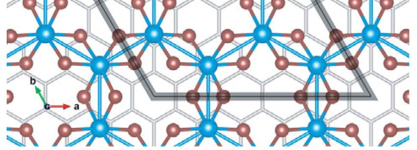
4

Majorana edge modes that appear at the interface be-            bands in twisted graphene bilayers is the starting point
tween the trivial and topological phases. This is shown         for realizing the Chern insulator states[55, 56].
in Fig. 1d, which shows an STM topographic image of                Flat bands in twisted bilayers can be interpreted as
CrBr3 island on a bulk NbSe2 substrate and three dI/dV          pseudo-Landau levels of an artificial gauge field, gen-
spectra (the signal is proportional to the local density of     erated by the modulated stacking in the unit cell[57].
states, LDOS, at the position of the STM tip): on the           Close to charge neutrality, these flat bands yield an 8-
NbSe2 substrate (blue), on the CrBr3 island (red) and           fold manifold, two-fold degeneracy coming from electron-
right at the edge of the island (green). The spectrum           hole states, two-fold coming from valley symmetry and
recorded on the island edge has a strong peak centered          two-fold coming from spin[55, 56, 58, 59]. As Landau
around the Fermi level (zero bias) consistent with the ex-      levels[57, 60], each flat band is expected to carry a non-
pected LDOS corresponding to the Majorana zero modes.           trivial Chern number, analogous to conventional Landau
Fig. 1e shows the measured (left) and theoretical LDOS          levels of quantum Hall states[61]. However, the origi-
(right) as a function of the energy. At the Fermi energy,       nal system is time-reversal symmetric, implying that flat
both the bulk phases are gapped, and only the Majorana          bands stemming from opposite valleys will carry oppo-
modes at the edges of the islands are visible. As the en-       site Chern numbers[57, 62]. This property suggests that
ergy is increased, we eventually start to see excitations       if valley symmetry is spontaneously broken, for exam-
in the topological superconductor with the edge modes           ple, due to electronic interactions, twisted graphene bi-
overlapping with bulk states. Finally, above the super-         layers become natural Chern insulators[63]. The break-
conducting gap, all significant LDOS contrast is lost.          ing of valley symmetry takes place when electronic inter-
   Comparison between theory and experiment allowed             actions create a spontaneous symmetry breaking, lead-
estimating the values of the model parameters, namely,          ing to a filling of just on the the valley flat bands. A
the induced magnetization in the top NbSe2 layer due            specific feature that must be taken into account is that
to the proximity of the CrBr3 layer and the magnitude           due to the existence of Dirac points in the electronic
of the Rashba spin-orbit coupling. These estimates sug-         structure[55, 56, 58, 59], leading to the Chern insula-
gest that the magnetization and the spin-orbit coupling         tor regime requires to first opening a gap at the Dirac
are of a similar magnitude, a few tens of meV. This val-        points[63–65]. This is done by taking aligned hBN layers
ues were also consistent with density-functional theory         with the twisted bilayer that induce a small symmetry
(DFT) calculations and in-line with proximity induced           breaking in the twisted bilayer lifting the original Dirac
exchange coupling in CrI3 /WSe2 and CrBr3 /MoSe2 het-           points. Ultimately, in the presence of partial filling, this
erostructures [48, 49]. Finally, the moiré pattern between      could lead to the emergence of fractional Chern states
CrBr3 and NbSe2 was suggested to further stabilize the          [66].
topological superconducting state[50].

                                                                     D.   Materials for artificial Chern insulators
            C.   Artificial Chern insulators
                                                                   These predictions were realized in twisted graphene bi-
   Chern insulators [54] represent another paradigmatic         layers with the twist angle (θ = 1.15◦ ) tuned to yield
state of matter in two-dimensional systems. Besides their       flat bands in the electronic spectrum [53, 55, 56]. The
conventional engineering by combining spin-orbit cou-           sample fabrication followed the usual “tear and stack”
pling and exchange fields [4], van der Waals materials          process [52, 67, 68], but TBG was aligned with the un-
offer a novel approach to engineered Chern insulators.          derlying h-BN layer. The alignment with BN turns out
This new approach to engineer Chern bands specifically          to be critical in lifting the low energy Dirac points, allow-
exploits moire patterns in twisted two-dimensional ma-          ing for the emergence of a valley polarized state. These
terials. The emergence of flat bands stems from a non-          state-of-the-art devices typically use TBG encapsulated
abelian elastic gauge field and will be further addressed in    by h-BN layers, and atomically smooth graphite flake
more detail in section IV E. As illustrated in Fig. 2a-c, the   is used as the gate electrode (see Fig. 2a). Finally, the
varying lattice registry in twisted bilayer graphene cre-       stack is electrically contacted using so-called edge con-
ates a long-wavelength moiré pattern. This moiré mod-           tacts, which have high transparency and avoid unwanted
ulation creates moiré mini-Brillouin zones at the K and         doping of the TBG [51]. Fig. 2d shows the longitudi-
K 0 points of the two graphene layers. These valleys are        nal (Rxx ) and the Hall (Rxy ) resistances measured as a
well-separated, and each valley hosts two Dirac cones of        function of the carrier density on a magic angle TBG
the same chirality. The Dirac cones living at the K 1 and       device at T = 1.6 K and under an external magnetic
K 2 (and at K 01 and K 02 ) hybridize, and when the respec-     field of B = +150 mT [53]. As expected for a quantum
tive Dirac points are sufficiently close to each other in the   Hall state, Rxy reaches h/e2 and Rxx approaches zero
k-space, this hybridization results in the formation of a       when the electron density is tuned to filling factor ν = 3
flat band with narrow bandwidth that is well separated          (ν, where ν is the number of the electrons in the flat
from other bands is formed as the twist angle θ is tuned        band per moiré unit w.r.t. no external doping, i.e. ν can
across the magic angle (Fig. 2c). This emergence of flat        have values between -4 and 4). The previous phenomena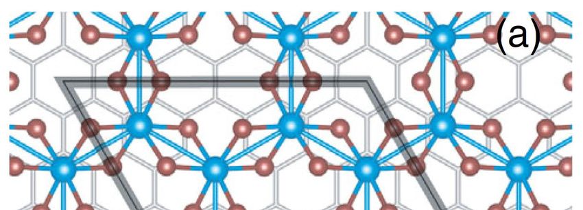
5

    a                                             c                             d
                                                                                                                                   d

                             b
                                                                                e                       f

FIG. 2. Chern insulating states in twisted bilayer graphene. (a) Illustration of a typical state-of-the-art device for TBG
transport experiment. TBG is sandwiched between two layers of h-BN and atomically smooth graphite flake is used as the
gate electrode. the contacts are so called edge contacts that have high transparency and avoid unwanted doping of the TBG
[51]. (b) The moiré modulation creates moiré mini-Brillouin zones at the K and K 0 points of the two graphene layers. These
valleys are well-separated and each valley hosts two Dirac cones of the same chirality. (c) Evolution of the band structure as
     https://www.nature.com/articles/nature26154/figures/1
the twist  angle is tuned. At the magic angle, a flat band with narrow band width that is well separated from other bands is
formed. Panels a-c from Ref. [52]. (d) Longitudinal (Rxx ) and the Hall (Rxy ) resistances measured as a function of the carrier
     https://journals.aps.org/prresearch/abstract/10.1103/PhysRevResearch.1.013001
density on a magic angle TBG device at T = 1.6 K and under an external magnetic field of B = +150 mT. (e) Rxx and Rxy
measured at the filling factor ν = 3 as a function of magnetic field B. (f) Schematic band structure at full filling of a moiré
unit cell (ν = 4) and ν = 3. Panels e-f from Ref. [53].

are the hallmarks of the QAHE state, and most impor-              the external magnetic field, the transition can be iden-
tantly it is retained in the absence of the field as shown        tified as a topological transition. Tracking the electron
in Fig. 2 - The Hall resistivity is hysteretic (Fig. 2e), with    densities at which these transitions happen as a function
a coercive field of several tens of millitesla. The Hall re-      of the magnetic field B, gives direct access to the asso-
                                                                                                  dn
sistivity is quantized (Rxy = h/e2 ) and the longitudinal         ciated Chern number C via dB       = C/Φ0 , where Φ0 is
resistivity remains small through zero external magnetic          the magnetic flux quantum. In addition to a host of lev-
field, which demonstrates that the quantum anomalous              els arising from the zeroth Landau level at ν = 0 with
Hall state is stabilized by spontaneously broken time-            Chern numbers C = 0, ±1, ±2, ±3, ±4, ±8, ±12, the au-
reversal symmetry. In particular, this time-reversal sym-         thors observe a hierarchy of correlated Chern insulating
metry breaking is purely associated to the valley sector,         phases with Chern numbers C = ±1, ±2, ±3 emerging as
where spontaneous symmetry-breaking leads just one of             a function of magnetic field from the different filling fac-
the valley filled as sketched in Fig. 2f. Finally, it worth to    tors ν = ±3, ±2, ±1, respectively. All these phases are
note that it is quite typical in the TBG experiments that         stabilized by a magnetic field.
the observed phenomena are device-specific, with minor               In addition to the example above, the Chern insulat-
differences in the device parameters being decisive which         ing state and the quantum anomalous Hall effect has also
states are formed. For example, robust, thermally acti-           been realized in rhombohedral (ABC-stacked) graphene
vated, trivial insulator behavior and the QAH state can           trilayers and twisted monolayer - bilayer graphene sam-
occur in very similar devices.                                    ples [70–72] and recent experiments on magic-angle bi-
   Typically, the Chern number can be estimated from              layers also suggest the possibility of realizing fractional
the value of the quantized Hall conductance, but this             Chern insulator states [73].
measurement requires working on a transport setup, and
it would be extremely interesting to be able to some-
how measure the Chern number directly and indepen-                       III.       VDW QUANTUM SPIN-LIQUIDS
dently. Precisely this was done by a scanning tunnel-
ing microscopy-based technique to directly measure the              Quantum spin-liquids[78, 79] are highly entangled
Chern numbers of the different Chern insulating states            quantum magnets, characterized by the emergence of
[69]. The topological gaps can be identified by measur-           novel fractionalized particles. These many-body states
ing the LDOS as a function of the electron density in             are classified to their pattern of long-range entangle-
the system (controlled through external doping) at dif-           ment. In terms of their excitation spectrum, quantum
ferent external magnetic fields. If the electron density at       spin-liquids can be classified in gapped or gapless, and
which gap opening and closing takes place depends on              in a minimal picture, this is ascribed to a gapless or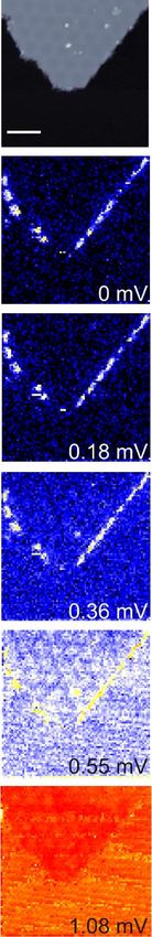
6

                         a                                   c

                         b                                       d

FIG. 3. (a) Sketch of a spin model with frustration stemming from anisotropic interactions. (b) Phase diagram of RuCl3 [74]
taking constant second and third neighbour exchange coupling. The red diamond indicates the estimated parameters for bulk
RuCl3 and the blue circle those for monolayer RuCl3 on graphene [74–76]. (c) The phase diagram of α−RuCl3 in an external
magnetic field at θ = 60◦ . Open and closed diamonds represent the onset temperature of zigzag type AFM order based on
thermal Hall conductivity measurements. A half-integer quantized plateau of the 2D thermal Hall conductance is observed
in the red area and open blue squares represent the fields where the thermal Hall response disappears [77]. (d) Top view of
α−RuCl3 /graphene heterostructure, where the blue and maroon spheres represent Ru and Cl atoms, respectively, and the gray
hexagon indicates the graphene monolayer [75].

gapped quasiparticle spinon excitations[79–81]. In ad-               tum spin-liquid models represents one of the open prob-
dition, quantum spin-liquids can be described by a de-               lems in many-body physics. A great amount of insight
confined gauge field theory [79, 82, 83], namely a theory            can, however, be obtained from finely tuned models that
that involves free spinons capable of propagating [84]. A            allow for an exact solution. Among these specially tuned
fundamental question is, which mechanisms capable of                 models, we encounter the Toric code and the anisotropic
driving a system from a magnetically ordered state to a              Kitaev honeycomb model[85]. In particular, the Kitaev
quantum disordered one can be designed.                              model realizes a highly anisotropic spin model in a hon-
                                                                     eycomb lattice that takes the form

 A.    QSL from frustrated anisotropic interactions
                                                                                               X
                                                                                          H=           Siγ Sjγ             (4)
   A first strategy to design quantum spin-liquids is to                                        hiji
focus on models showing highly directional interactions
that are inherently frustrated [85]. This can be done, for
example, by taking square [86] or honeycomb lattices[85],
and imposing anisotropic spin-spin interactions that are             where hiji denote first neighbors and γ labels the spin-
dependent on the bond considered. As magnetic interac-               component that interacts for each bond as depicted in
tions in materials are rotational symmetric in the absence           Fig. 3a). The genuine feature of the Kitaev honeycomb
of spin-orbit coupling, these mechanisms are expected to             model stems from the possibility of obtaining an exact
be realized in materials containing heavy atoms in which             solution in terms of single particle excitations. Remark-
spin-orbit effect compete and even overcome other inter-             ably, the single-particle excitation are of Majorana type,
actions present [87–90].                                             and depending on the parameter regime, realize gapless
   Due to their interacting nature, the solution of quan-            or gapped Majorana states[85].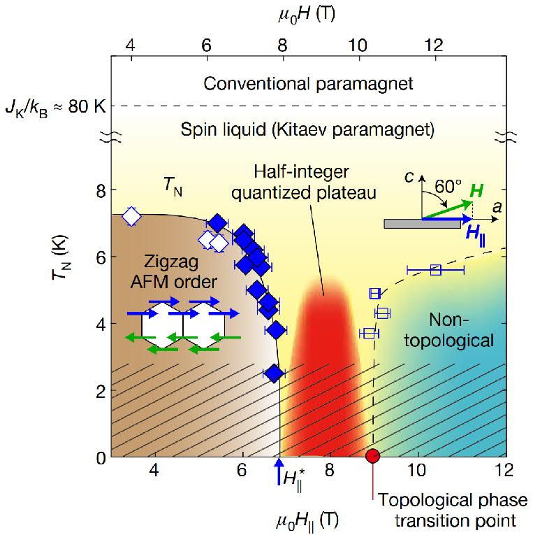
7

B.   Experiments QSL with anisotropic interactions             and doped in this heterostructure. This might even drive
                                                               an insulator-to-metal transition and help to realize pre-
   Interestingly, the Kitaev honeycomb model [85] (il-         dicted, exotic superconducting states in quantum spin-
lustrated in Fig. 3a) can be potentially adiabatically         liquids[75, 101]. In any case, the strain and doping are
connected to quantum spin-liquid states realized in α-         predicted to enhance the Kitaev interactions (increasing
RuCl3 (RuCl3 ) [74, 89, 91–93], and thus in the follow-        K and decreasing J and Γ) and move the system closer to
ing we will focus on this compound. RuCl3 is a lay-            the Kitaev. RuCl3 /graphene heterostructures have been
ered Mott insulator with significant spin-orbit interac-       also realized experimentally[102, 103], but not yet down
tions that is in the close proximity to the quantum spin-      to the monolayer limit. However, experiment on thicker
liquid ground state [66, 74, 75]. However, these materials     RuCl3 layers already give indications of the charge trans-
often host complex Hamiltonians having several contribu-       fer and hybridization between the RuCl3 and graphene
tions beyond the Kitaev exchange, including first, second      bands[102, 103].
and third neighbor exchange, and symmetric off-diagonal
exchange[74, 94–96]. The model typically employed for
this compound gives rise to the phase diagram sketched in                C.    QSL from geometric frustration
Fig. 3b as a function of the first neighbor couplings, keep-
ing the second and third neighbor exchange finite[74]. In
                                                                  Geometric frustration can lead to spin-liquid behavior
Fig. 3b, the x-axis represents the ratio of the Heisenberg
                                                               and considering a simple picture of three spins can give
(J) to Kitaev -type (K) spin coupling and Γ is symmetric
                                                               a flavor of the general idea: Consider three spins at the
off-diagonal exchange coupling. The whole diagram has
                                                               corners of a triangle with antiferromagnetic interactions.
been evaluated with the ratio of Hund’s coupling (JH )
                                                               This system does not have a configuration where all an-
to the Coulomb on-site interaction (U ) of JH /U = 0.2,
                                                               tiferromagnetic interactions can be simultaneously satis-
which can be estimated from ab initio calculations. It can
                                                               fied, i.e. the system is frustrated. This geometric frustra-
be seen that the phase diagram hosts ordered magnetic
                                                               tion leads to unusually large ground state degeneracies,
phases ranging from ferromagnetic (FM) and antiferro-
                                                               already at the classical level. The situation described
magnetic (AFM) to more complicated zigzag (ZZ), 120
                                                               above corresponds to a classically frustrated system, in
and incommensurate order (I) phases, even without con-
                                                               which quantum entanglement between sites is not consid-
sidering variations in the further neighbor exchange. The
                                                               ered and corresponds to the so-called spin ice models. In
best estimate for the parameters corresponding to bulk
                                                               the quantum realm, an effective strategy to realize quan-
RuCl3 is shown as a red diamond. This implies that the
                                                               tum spin-liquid physics is to focus on models realizing
ground state of RuCl3 is actually an ordered magnetic
                                                               non-bipartite lattices, such as triangular and kagome lat-
phase, which has been experimentally confirmed using,
                                                               tices. Kagome lattice models[104–106] have been known
e.g., thermal Hall conductance measurements[77].
                                                               to be a paradigmatic platform for quantum spin-liquid
   Remarkably, it was experimentally demonstrated that
                                                               physics. Since triangular lattices are often more common
applying a sufficient in-plane magnetic field can destroy
                                                               in the van der Waals world, we will in the following focus
the long-range order of the magnetic ground state and
                                                               on that case. Focusing on the triangular lattice model, in
give rise to quantum spin-liquid behaviour [77]. This is
                                                               the minimal case in which only first neighbor interactions
illustrated in the phase diagram shown in Fig. 3c, where
                                                               are considered, the ground state is actually an ordered
the boundaries of the different phases have been followed
                                                               state with 120 degrees spin spiral[107–109]. However,
using thermal Hall conductance measurements. Interest-
                                                               this model can be pushed to a more frustrated regime by
ingly, the Majorana edge modes that arise in the quan-
                                                               including additional interactions[110, 111], and in partic-
tum spin-liquid ground state can be directly verified as
                                                               ular, a second neighbor exchange coupling[112], driving
half-integer quantized thermal conductance, which is ob-
                                                               the system to a quantum spin-liquid ground state. Al-
served in the region shaded with red in Fig. 3c. Further
                                                               though an exact solution cannot be obtained in this limit,
increasing the lateral magnetic field gives rise to a phase
                                                               tensor network calculations have shown strong signatures
transition to some other non-topological phase.
                                                               of a gapless QSL liquid state in this regime, featuring
   In addition to the application of a lateral magnetic        gapless Dirac spinons.[112]
field, many other routes (e.g. external pressure and chem-
                                                                  The low energy excitations of these models in terms of
ical doping) are being tested to suppress magnetism, en-
                                                               chargeless emergent fractionalized excitations with S =
hance the pure Kitaev interactions and drive the sys-
                                                               1/2 known as spinons. We start with a Heisenberg model
tem towards the quantum liquid state. In the spirit of                            P        ~i · S
                                                                                                ~j where Si are the local spin
the designer material principles, we highlight a couple        of the form H = ij Jij S
of theoretical ideas where heterostructures could be used      operators. Assuming a quantum spin-liquid ground state,
to promote the quantum spin-liquid state. It has been          we can express the localized spins as emergent chargeless
                                                                                                                        †
                                                               S = 1/2 fermions of the form Siα = s,s0 σs,s       α
                                                                                                          P
                                                                                                                     0 fi,s fi,s0 ,
proposed that monolayer RuCl3 on graphene (illustrated
                                                                        †
in Fig. 3d) would result in a system with enhanced Ki-         where fi,s  denotes the creation operator of a fermionic
                                                                                      α
taev type interactions [75, 76]. By using ab initio cal-       spinon in site i, and σs,s0 are the spin Pauli matrices. The

culations, it was shown that the RuCl3 becomes strained        localized moment is implemented by enforcing having a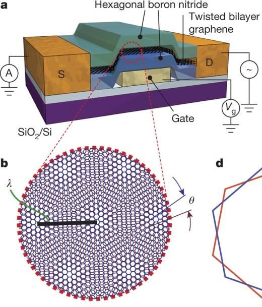
8

FIG. 4. (a) Schematic of a quantum-spin-liquid with frustration stemming from geometric frustration. (b) STM image recorded
on a buk 1T-TaS2 surface showing   √ the√characteristic “Star-of-David” charge-density wave pattern [97]. (b) Calculated band
structure of 1T-TaS2 with the 13 × 13 “Star-of-David” reconstruction and including the Ta spin-orbit coupling reveals a
single distinct split-off banb at the Fermi level (green line) [98]. Including the Hubbard U-term splits this band into a lower and
upper Hubbard band (d) STM dI/dV measurements on a related compound 1T-TaSe2 monolayer showing LHB and UHB [99].
The panels on the right show constant height dI/dV maps that allow direct visualization of the LHB and UHB wavefunction
symmetries. (e) Illustration of the low-temperature state of 1T-TaS2 with spatially random pairs of “Star-of-Davids” forming
singlets. It is possible to form gapless, low-energy fractional excitations (blue arrows) [100].

single fermion in each site f † f = 1. At the mean field            D.    Experiments on geometrically frustrated QSLs
level, the Heisenberg Hamiltonian a tight binding model
of free propagating S = 1/2 spinons of the form
                                                                      The necessary ingredients for a QSL - triangular lat-
                                                                   tice with frustrated magnetism (Fig. 4a) - can be real-
                                                                   ized in van der Waals materials. This has been demon-
                                                                   strated in the 1T phase of TaS2 (1T-TaSe2 is expected
                                                                   to be similar), where the presence of various charge-
                                     †                             density wave (CDW) states (depending on the temper-
                          X
                    H=          χij fi,s fj,s0             (5)
                           ij
                                                                   ature) has been known for some time [114–116].
                                                                                                               √      √ The
                                                                   low-temperature CDW state results in a 13 × 13 re-
                                                                   construction of the 1T-TaS2 lattice that has a 13 Ta atom
                                                                   “star of David” unit cell [97, 98, 114–116] as illustrated
where χij are the mean-field parameters of the mean-               in Fig. 4b. This causes folding of the band structure
field Hamiltonian. The spinon excitations of the quan-             and, together with modified hoppings caused by the re-
tum spin-liquid state can thus be understood from the              construction and the presence of spin-orbit coupling, re-
spinon dispersion. For example, gapless Dirac quantum              sults in a single band with a relatively flat dispersion at
spin-liquids have an associated spinon model featuring             the Fermi level (Fig. 4c) [98]. In the presence of strong
Dirac points,[112] whereas models with a finite spinon             electron-electron interactions (U larger than the band-
Fermi surface are stem from model with a finite Fermi              width of band at Fermi level), the system will undergo a
surface. This classification is often used when character-         Mott metal-insulator transition and instead of the single
izing quantum spin-liquid ground states, and has direct            band at the Fermi level, there will be a fully occupied
impact on the temperature-dependence of the thermal                lower Hubbard band (LHB) below the Fermi level and a
conductivity[113].                                                 fully unoccupied upper Hubbard band (UHB) above it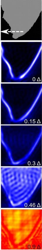
9

[117].                                                          states, which in the presence of any residual interactions
   In the case of 1T-TaS2 , this Hubbard band correspond        are expected to be prone to a variety of electronic insta-
to a single unpaired electron per CDW “star of David”           bilities [123–125]. In the following, we will discuss several
unit cell, which are the building block of the quantum          directions that van der Waals materials provide towards
spin-liquid state in this material. The Hubbard bands           the realization of flat band systems.
have been demonstrated in bulk 1T-TaS2 [97, 118] and
also in monolayer 1T-TaSe2 [99]. As illustrated for 1T-
TaSe2 in Fig. 4d, tunneling spectroscopy allows direct                A.    Generating flat bands from geometric
verification that the system is gapped and the energies                               frustration
of the LHB and UHB can be easily probed. In addition,
by mapping the spatial variation of the tunneling con-             The simplest instance in which flat bands appear in
ductance dI/dV ∝ LDOS, the spatial symmetries of the            electronic systems are tailored lattices leading to destruc-
states can be probed. In the case of 1T-TaSe2 monolayer,        tive interference[123, 126]. Paradigmatic examples of
it can be seen that the orbital texture of LHB and UHB          these flat band models are Lieb and kagome lattices[126].
are different (right side of Fig. 4d).                          In this system, electron propagation is quenched due to
   While STM and tunneling spectroscopy can be used             the existence of complementary paths that interfere de-
to probe the Hubbard bands, it is difficult to directly use     structively. This destructive interference can be often
these techniques to probe the spin-liquid state. This is        weakened by adding additional perturbations. For ex-
usually done with neutron scattering, where the “smoking        ample, next nearest neighbour (NNN) hoppings interac-
gun” for the QSL state is the lack of magnetic order down       tions will often cause the flat bands to acquire dispersion,
to the lowest temperatures. The other option is muon-           as flat bands are localized eigenstates on “disconnected”
spin-relaxation, which has been applied to bulk 1T-TaS2         lattice sites and NNN hoppings connect these sites and
to show that the spin excitations are gapless, and there is     make the flat band dispersive. In the case of the Lieb
no long-range order in temperatures of at least down to         lattice, the existence of a flat band can also be under-
70 mK [100]. Those experiments show that below 55 K,            stood from Lieb’s theorem[124]. In its general form, this
there is a broad distribution of the relaxation times indi-     theorem states that for a fully bipartite lattice, the num-
cating a highly inhomogeneous magnetic phase at all Ta          ber of flat bands will be |NA − NB |,[124] where NA is the
sites. This is strong evidence that there is growing ran-       number of removed sites from sublattice A, and NB the
domness in the spin system as temperature decreases be-         number of sites removed of sublattice B. In particular,
low 55 K. The observed slowing down of spin fluctuations        this implies that generic bipartite lattices in which one
is consistent with the freezing of singlets as illustrated in   site is removed will show a flat band. The Lieb lattice
Fig. 4e. Interestingly, for 1T-TaS2 the resonant valence        can be built by removing one site from the square lat-
bonds are formed between magnetic moments with an ex-           tice, leading to the existence of a flat band. In this very
tension of the enlarged unit cell generated by the CDW,         same fashion, other flat band models can be systemati-
in comparison with the atomic-like moments of bulk QSL          cally constructed by removing a certain number of sites.
candidates.                                                     These types of flat bands have been realized in artificial
   The problem with the bulk probes such as neutron             systems based on atomic lattices [127–131]. They can
scattering or muon spin-relaxation is that they are typ-        also be formed in suitable engineered, chemically syn-
ically not sufficiently sensitive to probe monolayer sam-       thesized lattices, where covalent organic frameworks and
ples. There are theoretical suggestions that tunneling          metal-organic frameworks are especially attractive sys-
spectroscopy could be used for this even though the mag-        tems for realizing these artificial models [132–140].
nitude of the predicted signal would depend on the mea-
surement geometry (e.g. 2D junction vs. STM) and
the type of the spin-liquid [120]. In addition, and de-             B.     Experiments flat bands from frustration
spite their chargeless nature, signatures of spinon inter-
ference can be potentially probed by inelastic transport           There have been many theoretical proposals on metal-
spectroscopy[121]. Finally, muon spin-relaxation has            organic frameworks (MOFs) with kagome structure that
been used to probe the Kondo effect with spinons[122],          should result in flat bands in their band structure
by probing the existence of a spinon-Kondo cloud around         [132, 133, 135]. However, the experimental demonstra-
magnetic impurities, and this technique could perhaps be        tion has proven difficult. If the assembly is carried out
extended to monolayer samples.                                  directly on a metal substrate (typically Au(111), Ag(111)
                                                                or Cu(111)), it is relatively straightforward to realize
                                                                MOFs with a large degree of structural perfection [134].
           IV.   NEW VDW FLAT BANDS                             Unfortunately, the relatively strong interaction with the
                                                                underlying metal substrate typically masks the intrin-
   The engineering of flat bands has been at the forefront      sic electronic structure of the MOF. On the other hand,
of condensed matter physics for a long time. Flat band          the formation of the high-quality MOFs on weakly in-
systems are characterized by having almost dispersionless       teracting substrates is much more challenging [141, 142]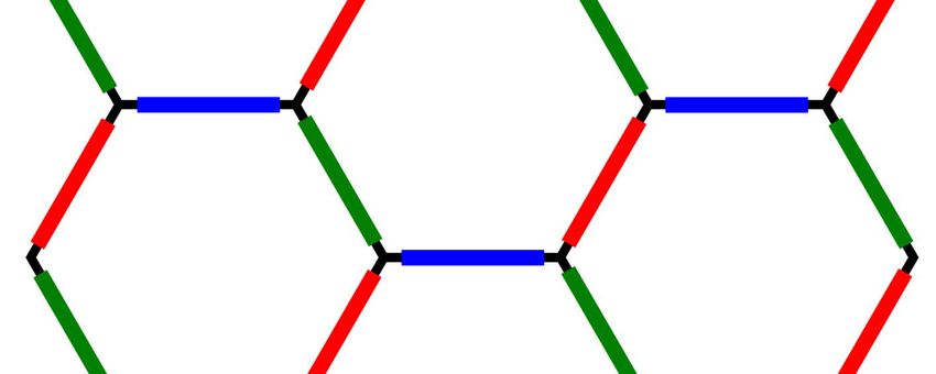
10

FIG. 5. Structure (a,c,e) and band structure (b,d,f) of different lattices featuring flat bands: the kagome lattice (a,b), the Lieb
lattice (c,d) and a modified honeycomb lattice (e,f). (g,h) Schematic and experimental structure of a π-conjugated polymer
poly-trioxaazatriangulene [119]. (i) Second-derivative ARPES signal of the sample shown in panel h acquired at a photon
energy of 120 eV. The dashed lines represent calculated bands for free-standing polymer netowrk, shifted downwards by 0.12
eV [119].

and unambiguous proof of the flat bands has not been                  C.   Generating flat bands from long wavelength
demonstrated.                                                                           modulations

                                                                      A simple way of generating nearly flat bands consists
   The other chemical strategy for synthesizing two-               of weakly coupling quantum dot states. In this picture,
dimensional networks on surfaces relies on the forma-              the bandwidth is determined by the coupling between
tion of covalent carbon-carbon bonds and structures                the quantum dots - the weaker it is, the flatter the re-
called covalent organic frameworks (COFs).           While         sulting bands will be. A convenient way of achieving this
there are extensive results on the formation of the one-           in a real material in a large scale is by exploiting moiré
dimensional nanocarbons (graphene nanoribbons) [131,               patterns [154–160]. The fundamental idea relies on the
143–147], challenges remain to create two-dimensional              locally modulated stacking over the moiré pattern that
assemblies with very high quality [148–150]. However,              causes a spatial modulation of the conduction and va-
there are recent experimental results that are pushing             lence band edges and leads the formation of a large scale
this field towards higher quality samples towards the for-         array of quantum dots in twisted van der Waals superlat-
mation of flat bands in the MOF or COF band structure              tices. The mechanism for flat band generation can be ra-
[119, 140, 142, 151]. The realized strategies rely on mak-         tionalized from the decoupled limit, in which the system
ing a molecular network with a kagome lattice with one of          consists of decoupled quantum dots. The twist angle be-
the examples highlighted in Fig. 5g-i. In particular, on-          tween the layers changes the size and separation between
surface polymerization was used to realize a high-quality          the quantum dots, promoting a finite hybridization be-
two-dimensional polymer poly-trioxaazatriangulene net-             tween them that leads to nearly flat bands[159, 161, 162].
work [119]. This sample was of sufficiently high qual-             It is worth noting that this mechanism holds when there
ity to allow angle-resolved photoemission spectroscopy             is a bandgap in the original materials (e.g. twisted h-BN
(ARPES) experiments that can be used to directly probe             and twisted dichalcogenide systems). This mechanism
the structure of the occupied bands as shown in Fig. 5i.           also requires the existence of a confinement gap. As a re-
This shows the folded bands of the valence band of the             sult, semimetals like graphene, in which electrons cannot
polymer that match the expected results well (calcu-               be electrostatically confined, require a different mecha-
lated bands shown by dotted lines). The kagome flat                nism for flat band generation. We will illustrate the use
band is expected to be at the bottom of the conduction             of gauge fields for this in section IV E.
band and cannot be directly probed by ARPES experi-
ments. These results are along the path towards tune-
able 2D organic or metal-organic structures with engi-                D.    Experiments flat bands from quantum dots
neered flat bands. The incorporation of metal atoms
with magnetism or a large spin-orbit interaction opens                As we discussed above, flat bands can be realized in
additional possibilities in realizing topological materials        gapped, twisted moiré systems and this has been demon-
[132, 133, 152, 153].                                              strated in several experiments. An early experiment by
11 Zhang et al. relied on direct growth of rotationally aligned WSe2 /WS2 moiré superlattices [166–168]. However, the MoS2 /WSe2 heterostructure, where the lattice mismatch moiré flat band systems can also have exciting optical then creates a moiré pattern [163]. While not directly effects and this has given birth to a field studying moiré resolving the flat bands spectroscopically, they demon- excitons [169–172]. strated that the system had the necessary ingredients for When the moiré period is larger than the exciton Bohr their existence: the modulated interlayer coupling giv- radius (around ∼ 1 − 2 nm in e.g. MoSe2 and WSe2 ), ing rise to a modulation of the conduction and valence the excitons will experience a spatially modulated pe- band edge energies. They showed that the valence and riodic potential from the moiré. The other design pa- conduction band edges are located at different layers and rameter in heterobilayers is the relative alignment of the that the local bandgap was periodically modulated with conduction and valence band edges, which allows the an amplitude of ∼ 0.15 eV, leading to the formation of a formation of intralayer excitons (e.g. WSe2 /WS2 sys- two-dimensional electronic superlattice. tem where the electron and the hole reside in the same The flat bands were directly identified in a later study layer [171]), interlayer excitons (e.g. MoSe2 /WSe2 system [164], which concentrated on a twisted bilayer WSe2 sam- where the electron and the hole exist in different lay- ples with twist angles of 3◦ and 57.5◦ . By using scanning ers [169, 170]) and hybridized excitons (e.g. MoSe2 /WS2 tunnelling spectroscopy, it was possible to directly map where the electron (for this system) is delocalized in the the spatial extent of the wavefunctions at the flat-band two layers [172]). Finally, the moiré-defined quantum energy and to show that the localization of the flat bands dots preserve the three-fold rotational (C3) symmetry, depends on the twist angle. The observed flat bands orig- which implies that e.g. the interlayer excitons should in- inated from the highest valence band at the Γ point (the herit valley-contrasting properties [169]. These systems conduction band onset varies very little over the moiré are currently under intense study to realize arrays of en- pattern and hence does not result in the type of quantum tangled quantum light emitters and realizing new exotic dot states required for the formation of the flat bands). excitonic many-body phases (e.g. topological exciton in- The flat band in 3◦ twisted bilayer is localized on the sulator) [173, 174]. hexagonal network separating the AA sites where as in the 57.5◦ systems, it is localized on the AB sites. These observations match well with the results of earlier atom- E. Generating flat bands from artificial gauge fields istic calculations [154]. While the basic physics of these systems can be under- A paradigmatic case of localized modes in a van stood with only considering the spatially varying stack- der Waals material is non-uniform strained graphene ing, in real materials, additional effects are expected to (Fig. 6a). The appearance of flat bands in this sys- take place. For example, it is likely that there are some tem stems from the emergence of an artificial gauge atomic-scale structural relaxations over the moiré pat- field[57, 62, 178]. The effect of strain is a create a term tern. This is precisely the effect that was assessed in in the system Hamiltonian that mimics a magnetic field the paper by Li et al. [165], who focussed on the twisted (“pseudo-magnetic field”). However, this differs from a WSe2 /WS2 system and used a combination of scanning real magnetic field as the artificial gauge field manifests tunneling spectroscopy (STS) experiments and ab ini- as a positive magnetic field for electrons in valley K and tio simulations of TMD moiré superlattices. They find a negative electric field for electrons in valley K’, so that a strong 3D buckling reconstruction together with large overall, the system does not break time-reversal symme- in-plane strain redistribution in their heterostructures. try. Using STS imaging, they identify different types of flat The simplest instance of this is periodically rippled bands originating either from the K-point at the valence graphene monolayers[179–183] (Fig. 6b). The emer- band edge or from the Γ-point that gives rise to more gence of the gauge field can be easily rationalized from deep-lying moiré flat bands. By analyzing the origin of the graphene Hamiltonian[62]. For unstrained graphene, these flat bands in detail, it is revealed that the K-point the low energy Hamiltonian in a single valley takes the flat bands are mainly a result of the deformation of the form[184] H = px σx + py σy . In the presence of a global monolayer. Similar behavior can be reproduced by con- uniform strain, the Dirac point get displaced from the sidering only a puckered monolayer WSe2 . On the other K and K’ points, leading to Hamiltonian of the form hand, the Γ-point flat bands are more in-line with the H = (px + Ax )σx + (py + Ay )σy . Now, in a non-uniformly idea of the moiré induced, weakly coupled array of quan- strained sample, we can take that there is a local strain tum dots. We will discuss the effects of periodic strain that changes in real space, turning Ax and Ay spatially in more detail in section IV E. dependent. Noting that A ~ enters in the Dirac Hamilto- The flat bands in the twisted TMD bilayers where the nian as a canonical momentum, we can then identify a electron kinetic energy is suppressed are of course, fertile strain-induced artificial magnetic field as B ~ = ∇ × A.~ ground for realizing systems where interactions play a Twisted graphene bilayers represent another case in dominant role. There have been several publications on which spatial modulations give rise to an artificial gauge e.g. realizing different kinds of correlated states, corre- field[57, 60]. In twisted graphene bilayers, the stacking in lated insulators and Wigner crystals in WSe2 /WSe2 and space changes between AA, AB and BA. The modulation
12

FIG. 6. Sketch of the buckling of a graphene monolayer (a) and spatial profile of the induced gauge field (b) [175]. Change in
the local structure of a graphene bilayer leading to a non-abelian gauge field (c) [57], and profile of the stacking in the moire
unit cell (d). Panels (ef) shows the topography (e) and dI/dV (f) of buckled graphene monolayer, showing the emergence of
pseudo Landau levels.[176] Panel (f,g) shows the real-space STS (f) and dI/dV (g) of a twisted graphene bilayer at 1.8◦ , showing
the emergence of van Hove singularities associated to non-abelian Landau levels.[177]

of the interlayer hopping due to the stacking brings up           the effects of pseudomagnetic fields and how they can
localized modes stemming from gauge fields, that can be           confine the charge carriers in graphene [188, 189].
rationalized as follows. A local Hamiltonian for a bilayer
can be represented by a 4 × 4 Hamiltonian, in which the
off-diagonal blocks contain the coupling between the two
                                                                     The buckling of graphene monolayers can also be cre-
layers. Due to the modulated stacking (Fig. 6cd) the
                                                                  ated by choosing an appropriate substrate. In particular,
2×2 interlayer coupling is modulated in space. Given the
                                                                  recent experiments of graphene on top of NbSe2 showed
Dirac nature of the monolayer dispersion, that modulated
                                                                  that graphene gets a spontaneous buckling on this struc-
hopping can be rationalized as an off-diagonal 2×2 gauge
                                                                  ture. Associated to the buckling, a periodic non-uniform
field, namely a non-abelian SU (2) gauge field[57]. This
                                                                  strain appears in the graphene monolayer, which gives
non-abelian gauge field will thus give rise to associated
                                                                  rise to an elastic gauge field spontaneously[180, 182, 190].
pseudo Landau levels, the lowest one of them being the
                                                                  Signatures of pseudo-Landau levels in this spontaneously
magic-angle flat bands at 1◦ [55, 56, 60].
                                                                  buckled structure have been recently observed with
                                                                  STM[176].

    F.   Experiments flat bands from gauge fields
                                                                     The second example of pseudo-Landau levels corre-
   The earliest experiments showing the emergence                 sponds to twisted bilayer graphene. Signatures of the
of pseudo-Landau levels appeared in non-uniform                   lowest pseudo-Landau level, usually known as magic an-
strained graphene, which naturally appear in graphene             gle flat bands we observed early on, including some signa-
nanobubbles[185]. In these setups van Hove singularities          ture of symmetry breaking[177, 191, 192]. In particular,
in the density of states were shown to appear, in con-            these pseudo-Landau-levels show a strong localization at
trast with the semimetallic spectra of unstrained sam-            the AA stacking regions of the twisted bilayer[177]. In-
ples. The emergence of those resonances is associated             terestingly, higher index Landau levels can also lead to
to the emergent gauge field, which was shown to cor-              correlated states[193], show different localization in the
respond to up to an effective field of 300 T[185]. These          moire unit cell, and in particular the next van Hove
nanobubbles can also be realized with graphene deposited          singularity shows a higher extension around the AA
on a weakly interacting substrate, and in that case, the          regions[177, 191, 192]. Subsequent experiments have fur-
STM tip could be used to tune the strain and hence,               ther explored the nature of the lowest flat band, in partic-
the pseudo-magnetic field [186, 187]. Finally, suspended          ular, observing spontaneous rotational symmetry break-
graphene drumheads have also been used to investigate             ing due to electronic interactions[194].
13
V. OUTLOOK of topologically non-trivial flat bands in twisted van der
Waals materials provides an ideal starting point for frac-
tional quantum Hall states in the absence of magnetic
The possibility of artificial engineering states of matter field, known as fractional Chern insulators[66, 201–204].
with van der Waals materials has demonstrated a huge Analogous phenomenology for flat bands hosting spin-
potential in the last few years. Beyond the instances textured bands would further provide playgrounds for
of topological insulators and superconductors, quantum fractional quantum spin Hall physics, a state not found
spin-liquids and flat band physics, their tunability opens in nature yet. Ultimately, the combination of potential
prospects potentially opening radical new directions in fractional quantum Hall physics and superconductivity
quantum matter. in twisted multilayers provides an ideal starting point
Starting with topological superconductors, a challenge for engineering novel parafermion states[205, 206]. These
for future experiments will be to braid the emergent Ma- states have resisted experimental realization so far due to
jorana modes, in an analogous way as it has been pro- the difficulty of having simultaneously fractional quan-
posed for semiconductor nanowires[17, 18]. The possibil- tum Hall physics and superconductivity due to the large
ity of switching on and off topological superconductiv- magnetic fields required. Such limitation would, however,
ity with local gates provides a direction for extending not exist for intrinsic fractional quantum Hall states in
these schemes to two-dimensional materials. Further- graphene multilayers, providing an ideal solid state plat-
more, artificial engineering can also allow engineering form for parafermion physics.
higher-order topological superconductors, in which the Advances in the last few years have drastically proved
braiding of corner modes[195, 196] can open up a po- the versatility of artificial engineering in van der Waals
tential new direction for topological quantum computing materials, revealing a variety of exotic phenomena previ-
with van der Waals materials. ously only observed in rare compounds. While many of
those proposals require further materials engineering and
Quantum spin-liquids open up exciting new experi- to further understand the physics of the underlying ma-
mental possibilities well beyond their experimental con- terials, the steady development of the field suggest that
firmation. First, the emergence of fractional spinon ex- some of those goals may be achieved in the near future.
citations in these systems opens possibilities to control-
lable spinon transport, and ultimately its interface with
current spintronic devices[197, 198]. Secondly, the emer- ACKNOWLEDGMENTS
gence of anyonic excitations in certain quantum spin
liquids[199, 200] motivate potential future application of
We thank our group members - past and present - and
these systems for topological quantum computing[200].
colleagues for inspiration and insightful discussions. We
Flat band systems further offer novel possibilities for acknowledge support from the European Research Coun-
emergent quantum matter, going beyond the well-known cil (ERC-2017-AdG no. 788185 “Artificial Designer Mate-
possibilities for high-temperature superconductivity and rials”) and Academy of Finland (Academy professor fund-
symmetry broken states. In particular, the emergence ing no. 318995 and Academy research fellow no. 331342).
[1] Xiao-Liang Qi and Shou-Cheng Zhang, “Topological in- [7] A Yu Kitaev, “Unpaired majorana fermions in quantum
sulators and superconductors,” Rev. Mod. Phys. 83, wires,” Physics-Uspekhi 44, 131–136 (2001).
1057–1110 (2011). [8] Roman M. Lutchyn, Jay D. Sau, and S. Das Sarma,
[2] M. Z. Hasan and C. L. Kane, “Colloquium: Topological “Majorana fermions and a topological phase tran-
insulators,” Rev. Mod. Phys. 82, 3045–3067 (2010). sition in semiconductor-superconductor heterostruc-
[3] Yoichi Ando, “Topological insulator materials,” J. Phys. tures,” Phys. Rev. Lett. 105, 077001 (2010).
Soc. Jpn. 82, 102001 (2013). [9] Yuval Oreg, Gil Refael, and Felix von Oppen, “Helical
[4] Chao-Xing Liu, Shou-Cheng Zhang, and Xiao-Liang liquids and Majorana bound states in quantum wires,”
Qi, “The quantum anomalous Hall effect: Theory and Phys. Rev. Lett. 105, 177002 (2010).
experiment,” Annu. Rev. Condens. Matter Phys. 7, 301– [10] Liang Fu and C. L. Kane, “Superconducting proximity
321 (2016). effect and Majorana fermions at the surface of a topo-
[5] Jason Alicea, “New directions in the pursuit of Majo- logical insulator,” Phys. Rev. Lett. 100, 096407 (2008).
rana fermions in solid state systems,” Rep. Prog. Phys. [11] Liang Fu and C. L. Kane, “Josephson current
75, 076501 (2012). and noise at a superconductor/quantum-spin-hall-
[6] Shawulienu Kezilebieke, Md Nurul Huda, Viliam Vaňo, insulator/superconductor junction,” Phys. Rev. B 79,
Markus Aapro, Somesh C. Ganguli, Orlando J. Sil- 161408 (2009).
veira, Szczepan Głodzik, Adam S. Foster, Teemu Oja- [12] C.W.J. Beenakker, “Search for Majorana fermions in
nen, and Peter Liljeroth, “Topological superconductiv- superconductors,” Annu. Rev. Condens. Matter Phys.
ity in a van der Waals heterostructure,” Nature 588, 4, 113–136 (2013).
424–428 (2020). [13] A. K. Geim and I. V. Grigorieva, “Van der Waals het-You can also read