Zinc oxide light-emitting diodes: a review - SPIE Digital Library
←
→
Page content transcription
If your browser does not render page correctly, please read the page content below
Zinc oxide light-emitting diodes: a
                 review

                 Faiz Rahman

                                  Faiz Rahman, “Zinc oxide light-emitting diodes: a review,” Opt. Eng. 58(1), 010901 (2019),
                                  doi: 10.1117/1.OE.58.1.010901.

Downloaded From: https://www.spiedigitallibrary.org/journals/Optical-Engineering on 07 Sep 2021
Terms of Use: https://www.spiedigitallibrary.org/terms-of-use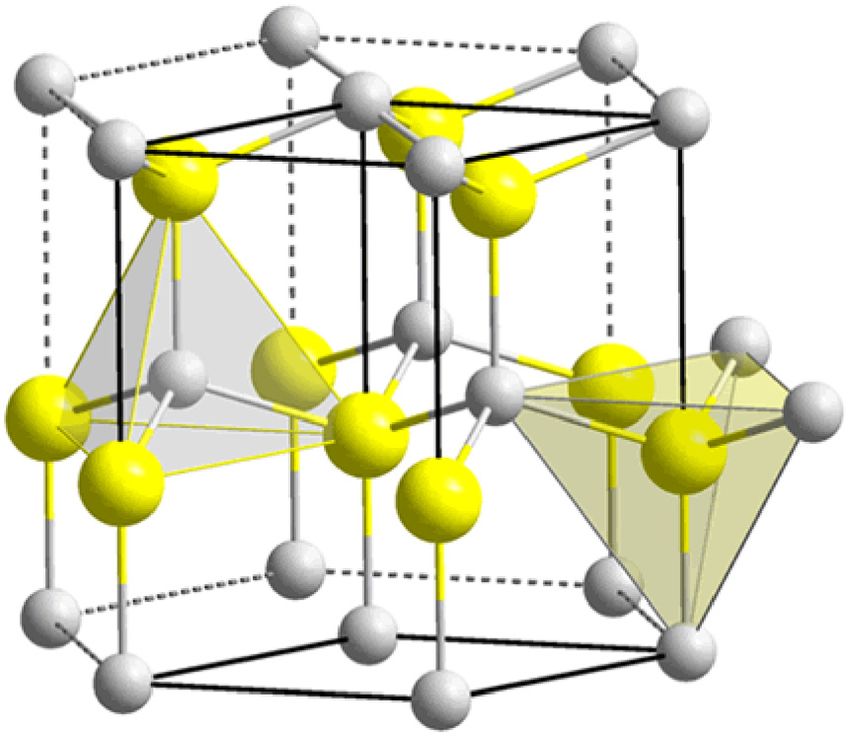
Optical Engineering 58(1), 010901 (January 2019)
                                                                                                                                                  REVIEW

                Zinc oxide light-emitting diodes: a review
                Faiz Rahman*
                Ohio University, Russ College of Engineering and Technology, School of Electrical Engineering and Computer Science, Athens, Ohio,
                United States

                              Abstract. This paper presents a compact survey of the various material schemes and device structures
                              that have been explored in the quest toward developing light-emitting diodes (LEDs) based on zinc oxide
                              (ZnO) and related II-oxide semiconductors. Both homojunction and heterojunction devices have been surveyed.
                              Material for fabricating these devices has been grown with a number of different techniques, such as pulsed
                              laser deposition, molecular beam epitaxy, metal-organic chemical vapor deposition, and atomic layer epitaxy.
                              This review also features a self-contained introduction to materials science and device processing
                              technologies that are relevant for fabricating ZnO LEDs. These topics include dry and wet etching, contact
                              formation, and optical doping of ZnO. Due to the overwhelming importance of p-type doping of ZnO for making
                              electronic and optoelectronic devices, a separate short section on electrical doping of ZnO is also included.
                              The rest of this paper describes several different attempts at making blue- and ultraviolet-emitting ZnO
                              LEDs. These include simple pn-junction devices as well as more complicated heterostructure devices
                              incorporating charge carrier barriers and quantum wells. © 2019 Society of Photo-Optical Instrumentation Engineers (SPIE)
                              [DOI: 10.1117/1.OE.58.1.010901]
                              Keywords: zinc oxide; light-emitting diode; oxide semiconductors; semiconductor heterostructures.
                              Paper 181495V received Oct. 24, 2018; accepted for publication Dec. 18, 2018; published online Jan. 17, 2019.

                1 Introduction                                                                    LEDs made from ZnO have received the most attention to
                Advances in the technology of electronic and optoelectronic                       date and the aim of this focused review is to highlight the
                devices are often a result of the development of new material                     various approaches that have been taken in recent years to
                systems with properties that are superior to those of existing                    fabricate both heterojunction and homojunction ZnO LEDs.
                materials. This happened when silicon replaced germanium                          The high binding energy of excitons in ZnO, relative to
                in the early years of the semiconductor industry. Another                         thermal energy at room temperature, makes ZnO LEDs and
                time this happened was when gallium arsenide emerged as                           diode lasers potentially brighter than comparable devices
                a semiconductor of choice for building extremely fast devi-                       made from other semiconductors. This can have dramatic
                ces. A similar development may be in the offing for optoelec-                     consequences for near- and mid-ultraviolet (UV) emitters
                                                                                                  where GaN has not performed so well in terms of cost
                tronics this time with the advent of zinc oxide (ZnO). This is
                                                                                                  and device efficiency. If potential problems with ZnO family
                a promising material that might one day substantially replace
                                                                                                  semiconductors, as outlined later in this paper, could be
                gallium nitride (GaN) as the material of choice for making
                                                                                                  overcome then high-brightness solid-state light sources will
                short-wavelength light emitters and detectors. ZnO—a II–VI
                                                                                                  become possible for such budding applications as water puri-
                oxide semiconductor—possesses properties that are broadly                         fication, resin cross-linking, microprinting, high-density data
                similar to that of GaN, which is now almost universally used                      storage, non-line-of-sight optical communication, and indoor
                for making blue light-emitting diodes (LEDs) and violet                           plant growth, to name a few. However, in order to enable
                lasers, as well as a number of other devices. A number of                         these advances and to open new markets, considerable work
                years ago, GaN emerged as the leading material from which                         still needs to be done to perfect the art of making high-
                short-wavelength optoelectronic devices are fabricated. Its                       quality ZnO-based pn-junctions.
                dominance has remained unchallenged so far and has only                               We start with a brief mention of the steadily increasing
                grown with further advances in the technology of III-nitrides.                    importance of solid-state lighting during recent years. This
                ZnO now appears to have the potential to challenge the pre-                       technology has been driven by the emergence of the blue-
                eminence of III-nitrides, but whether it lives up to its promise                  emitting GaN-based LED, but ZnO could surpass it if the
                in the coming years will depend on whether the considerable                       technical problems associated with its controlled doping
                challenges that remain before this material becomes indus-                        are successfully solved in the coming years. Next, we
                trially useful could be overcome in an acceptable manner.                         look at the material properties and device fabrication tech-
                Mere laboratory advances will not be sufficient—robust                            nologies that are relevant for making LEDs out of II-oxides
                and reliable processes will have to be developed that                             centered on ZnO. A good understanding of these topics is
                could be used to routinely fabricate efficient, stable, and                       essential for fabricating working ZnO LEDs. A short section
                long-lived devices on a large scale. Nevertheless, working                        that mentions the problem of p-type doping of ZnO comes
                devices have been built from ZnO and related materials                            next. This has remained as the central issue that has, so far,
                that show the potential inherent in this material system.                         precluded the realization of commercial ZnO LEDs. After
                                                                                                  that we survey the work that has been done by several groups
                                                                                                  around the world to demonstrate working ZnO LEDs—both
                *Address all correspondence to Faiz Rahman, E-mail: rahmanf@ohio.edu              heterojunction and homojunction. This review ends with

                Optical Engineering                                                       010901-1                                      January 2019   •   Vol. 58(1)

Downloaded From: https://www.spiedigitallibrary.org/journals/Optical-Engineering on 07 Sep 2021
Terms of Use: https://www.spiedigitallibrary.org/terms-of-use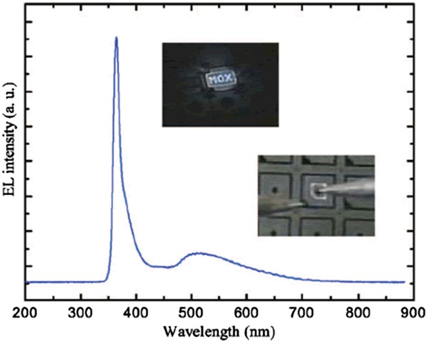
Rahman: Zinc oxide light-emitting diodes: a review

                a brief end note outlining the current status of ZnO LEDs and                     has enabled bright and energy-saving white light sources.”
                the need for further progress in this field.                                      GaN-family semiconductors possess favorable set of proper-
                                                                                                  ties that enable their use for making blue and UV LEDs and
                                                                                                  laser diodes. However, technology never remains still and for
                2 Solid-State Lighting with Wide Bandgap                                          many years, researchers have wondered about other possible
                   Semiconductors                                                                 materials for generating short-wavelength visible and invis-
                Since the mid-1990s, high-power white LEDs capable of                             ible radiation. Of the several possibilities, ZnO clearly stands
                space illumination have become widely available. A radical                        out because of its many similarities to GaN as well as some
                departure from conventional means of generating light,                            superior features. Thus it is not surprising that despite con-
                LEDs have features that make them especially suited for                           tinuing difficulties in ZnO technology many attempts have
                lighting applications. Their small size, high efficiency in                       been made at constructing working LEDs from this material.
                converting electrical energy to light, absence of radiated
                heat and UV, availability in many colors (including white),                       3 ZnO Material and Process Technology
                and the absence of environmentally harmful substances that                        For the purposes of this survey, it is best to begin by briefly
                might pose a problem during disposal, make them ideal as                          looking at some of the salient properties of ZnO. Interest in
                light sources for almost any conceivable illumination                             this material for its electrical properties dates back to the
                application.1,2 Little wonder than that LED-based luminaires                      1920s when it was investigated as a possible “crystal” for
                are finding increasing acceptance all over the world. From                        making cat’s whisker diodes during the early days of wire-
                domestic light bulbs to car headlights and from projector                         less communications. For its other applications, of course,
                lamps to light sources for horticulture, we now find LEDs                         ZnO has been known from prehistoric times; mostly as
                being used in all walks of life. The market for LEDs and                          a white pigment, that to this day is the constituent of most
                solid-state lighting systems has been growing at close to                         water color palettes. The electronic properties of ZnO began
                25% per annum for the past several years and by all indica-                       to be investigated, both theoretically and experimentally,
                tions will continue to do so for the foreseeable future.                          with the dawn of the semiconductor age in the late 1940s.
                    LEDs for space lighting applications are mostly based on                      Materials scientists and crystallographers, metallurgists
                blue-emitting GaN LEDs pumping a color-converting                                 and physicists, all had a go at investigating its properties.
                phosphor. The phosphor—usually, but not always, based                             What we know today about ZnO is a result of both early
                on a rare-earth-doped wide bandgap insulator host—is the                          and on-going explorations of the properties of this remark-
                luminescent material that down-converts much of the blue                          able material.
                pump light around 450 to 470 nm to longer wavelengths in
                the yellow and red region. The combination of this long
                wavelength emission with the residual (unconverted) blue                          3.1 Structure of ZnO
                light appears white to human eyes. Many advances have                             The structure of crystalline ZnO was investigated as far back
                been made in the science and technology of phosphors for                          as in 1935.6 ZnO crystallizes with the Wurtzite structure
                LED applications, and, as a result, today’s white LEDs emit                       (a hexagonal crystal structure, often adopted by binary sul-
                light of much superior quality than was the case just a few                       phides and oxides). In this crystalline form zinc ions, Zn2þ
                years ago.3 During the first few years after the appearance of                    are found on the sites of a hexagonal close packed sublattice
                LED light bulbs, their consumer acceptance was mainly lim-                        interpenetrated by a similar lattice populated with oxygen
                ited by the inferior quality of their light output. To many                       ions O2− . The hexagonal unit cell is characterized by lattice
                users, their light appeared too cold and markedly different                       parameters of a ¼ 3.25 Å and c ¼ 5.21 Å. This arrange-
                from that given off by incandescent lamps. The bluish hue                         ment is such that each zinc ion is surrounded by a tetrahedron
                of those early white LEDs was due to the use of cheap nar-                        of four oxygen ions and similarly each oxygen ion is coor-
                rowband phosphors. This remained an issue for several years                       dinated by a tetrahedron of four zinc ions (see Fig. 1). As
                until LED manufacturers developed better LED phosphors.                           a result of this tetrahedral coordination, ZnO has a polar
                The new phosphors employ multiple rare-earth ions in the                          character, giving rise to spontaneous electric polarization
                same host or make use of a carefully balanced mixture of                          (as is also the case with GaN). The consequent piezoelectric
                different phosphors. The rich broad spectrum of white                             properties of ZnO are important for understanding the behav-
                light from current generation of LEDs is making solid-sate                        ior of ZnO-based devices as this material is even more piezo-
                lighting proliferate in all kinds of lighting applications.4,5                    electric than GaN. The tetrahedral coordination seen in ZnO
                While phosphors are undoubtedly extremely important for                           is also an indicator of sp3 bonding and indeed ZnO has
                LEDs, the pump chip is no less important. Principally, this                       a mixed ionic-covalent character with nearly equal contribu-
                is because the efficiency of the pump chip determines, to                         tion from each bonding type. This feature gives rise to
                a large extent, the overall energy conversion efficiency and                      some interesting chemical reactions that are possible with
                efficacy of phosphor-converted LEDs. This is where alterna-                       this oxide.
                tive materials, such as ZnO, can play an important role.
                    Commercial quality, blue-emitting diodes based on
                III-nitride technology were first developed in Japan during                       3.2 Properties of ZnO
                the 1980s and 1990s. The early pioneering demonstrations                          As a semiconductor, ZnO is a direct bandgap II–VI oxide
                gave rise to the entire multibillion dollar solid-state lighting                  semiconductor with the minimum separation between the
                industry of today. This fact was appropriately recognized                         valence band and conduction band edges of 3.37 eV at room
                when the 2014 Nobel Prize in Physics was jointly awarded                          temperature. The large bandgap classifies ZnO as a wide
                to Isamu Akasaki, Hiroshi Amano, and Shuji Nakamura “for                          bandgap semiconductor. The rather large bandgap results
                the invention of efficient blue light-emitting diodes, which                      in ZnO being transparent to visible radiation and thus

                Optical Engineering                                                       010901-2                                       January 2019   •   Vol. 58(1)

Downloaded From: https://www.spiedigitallibrary.org/journals/Optical-Engineering on 07 Sep 2021
Terms of Use: https://www.spiedigitallibrary.org/terms-of-use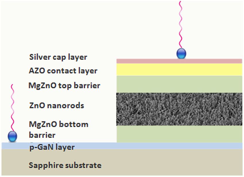
Rahman: Zinc oxide light-emitting diodes: a review
absence of bulk substrate for epitaxial growth. In the absence
of a native substrate, GaN is grown on sapphire as the next
best substrate material. However, the 15% lattice mismatch
between GaN and sapphire results in a high density of
interfacial dislocations that seriously compromise device
performance. Although free-standing GaN wafers have now
become available, these are currently quite expensive and
are thus suitable only for making more expensive devices
such as laser diodes. Bulk ZnO wafers, in comparison,
have been readily available for quite some time because
this material can be grown through a variety of routes,
such as hydrothermal growth.7,8 The density of hydrother-
mally grown ZnO9 is close to 5.6 g∕cm3 , corresponding
to 4.2 × 10²² ZnO units∕cm3 . High-quality, single- and
double-side polished ZnO wafers are now commercially
available from several suppliers. These provide an ideal sub-
strate for subsequent epitaxial growth, free from threading
Fig. 1 Lattice structure of ZnO showing Zn2þ ions (yellow) and dislocations that rob GaN-based devices of much of their
O2− ions (gray). application potential. It is interesting to note that, due to
a lattice mismatch of just 1.8% and similar chemical struc-
polished single crystals of ZnO, on cursory examination, tures, GaN and ZnO can be epitaxially grown on each
appear just like pieces of ordinary glass (see Fig. 2). The other.10,11 This raises the interesting possibility of combined
bandgap of ZnO is almost the same as that of GaN and GaN–ZnO hybrid devices and indeed most heterojunction
thus these two semiconductors share many physical proper- ZnO LEDs demonstrated so far, as we shall see later in
ties; though there are also many dissimilarities. this paper, have been such hybrids.
ZnO has certain superior attributes compared to GaN
when it comes to making optoelectronic devices. To begin, 3.3 Wet Etching of ZnO
ZnO is an environmentally friendly material because zinc is The chemical nature of ZnO is such that it can be easily
both plentiful in the earth’s crust and is nontoxic to humans. etched through wet chemical processes. While dry etch
The biocompatibility of ZnO has led to its use in many oral chemistries are available for ultrasmall features, where
and topical medicines. Gallium in GaN, on the other hand, is needed (such as simple CH4 -based chemistries—see below),
a relatively scarce and heavy metal, which is toxic to many devices could be fabricated by simpler wet etching
humans. Unlike GaN, ZnO requires no special handling or processes.12–14 In many cases, even submicron features
disposal considerations. More importantly for device fabri- can be etched with acidic etchants, such as dilute ortho-
cation, until recently, GaN has suffered from a well-known phosphoric acid, containing appropriate surfactants. Ferric
chloride and oxalic acid also work very well for etching
ZnO.12 GaN, in contrast, is very difficult to etch through
wet chemistries although some attempts have been reported
in the literature.15,16
3.4 Dry Etching of ZnO
Good process capabilities have also been developed for dry
etching of ZnO. Both chlorine-based and hydrocarbon-based
dry etch chemistries for ZnO have been investigated by
a number of research groups. Ip et al.17 reported results
on inductively coupled plasma (ICP) dry etching of
high-quality bulk single-crystal ZnO samples with both
CH4 ∕H2 ∕Ar and Cl2 ∕Ar plasmas. At low ion energies,
the former gives faster etching while the latter takes over
in the etch rate at higher ion energies. In the case of meth-
ane-based chemistry, low ion energies are not very effective
because breaking the high bond strength of Zn–O bonds
requires high-energy ion impacts. However, once the
bonds are broken, ZnO can volatilize as the dimethyl zinc
species: ðCH3 Þ2 Zn. The high vapor pressure of this com-
pound (301 mTorr at 20°C) is the cause of the high-ultimate
etch rate seen with methane-based chemistries. On the other
hand, for ZnCl2 formed with chlorine-containing chemis-
tries, the etch product has a lower vapor pressure of about
1 mTorr at 428°C consistent with the slower etch rates
Fig. 2 Hydrothermally grown, 1 cm2 , 2-mm thick, h0001i oriented, seen with this chemistry. Ip et al. also found that the
undoped ZnO wafers. near-surface stoichiometry of ZnO was unaffected by
Optical Engineering 010901-3 January 2019 • Vol. 58(1)
Downloaded From: https://www.spiedigitallibrary.org/journals/Optical-Engineering on 07 Sep 2021
Terms of Use: https://www.spiedigitallibrary.org/terms-of-use
Rahman: Zinc oxide light-emitting diodes: a review

                CH4 ∕H2 ∕Ar etching, as measured by Auger electron spec-
                troscopy. That led them to conclude that the CH4 ∕H2 ∕Ar
                plasma chemistry is capable of equirate removal of the Zn
                and O etch products during ICP dry etching. This ion-
                assisted nature of ZnO dry etching creates nice vertical
                side-wall profiles. Also because the near-surface stoichiom-
                etry is maintained, so the etching process produces only
                a small degree of surface roughening. Additional work on
                ICP etching of ZnO using methane-based chemistry, carried
                out in South Korea by Lee et al.,18 has also corroborated
                these findings. The effect of the inert gas used in the etching
                gas mixture was investigated by Lim et al.19 at the University
                of Florida. They found higher etch rates when using Ar or Xe
                than with He, which again highlights the role of effective
                momentum transfer in breaking the strong Zn–O bonds.
                                                                                                  Fig. 3 Photonic crystal light extraction structure etched into the top of
                While pure chlorine-based plasmas are considerably slow                           a GaN light-emitting device.
                at etching ZnO, derived chemistries such as those based
                on BCl3 have been shown to be more effective. Kim et al.20
                investigated ZnO etch rates as a function of BCl3 ∕Cl2 ∕Ar,                       extraction structures on ZnO devices are shallower and easier
                BCl3 ∕Ar, and BCl3 ∕CH4 ∕H2 chemistries. They found that                          to fabricate than those on GaN devices (see Fig. 3 for an
                compared with Ar, Cl2 ∕Ar, and CH4 ∕H2 -based gas mix-                            example of photonic crystal structure on a GaN light-emit-
                tures, pure BCl3 gas results in substantially high etch                           ting device). This should lead to brighter devices that have
                rates; indicating that B and BCl radicals react with ZnO                          a convincing external quantum efficiency advantage over
                and form volatile compounds such as Bx Oy and/or species                          GaN-based devices.
                containing BCl–O bond.21 The oxygen is thus removed                                  Perhaps the most often cited advantage of ZnO over GaN
                by boron, whereas zinc is removed concomitantly by chlo-                          for making LEDs is the higher excitonic energy in the II-
                rine, with the formation of ZnCl2 . It should also be men-                        oxide system.34,35 ZnO has an exciton binding energy close
                tioned here that dry etching can cause both mechanical                            to 60 meV, more than twice that of the 20- to 25-meV value
                and radiation damage to most materials but ZnO is excep-                          for GaN. Thus light emitting devices made from ZnO should
                tionally radiation-hard and can tolerate high amounts of                          be brighter than comparable GaN-based devices at the same
                irradiation without significant damage.22                                         operating current. In other words, ZnO-based light emitters
                                                                                                  should be more efficient when compared with similar GaN-
                3.5 ZnO as a Transparent Conductive Oxide                                         based devices. This also means that laser diodes made out of
                                                                                                  the ZnO system should have lower threshold current require-
                Heavily aluminum-doped ZnO (Al:ZnO; also referred to as                           ment when compared with GaN-based laser diodes.
                AZO) is transparent and exhibits high metallic conductivity.
                This transparent conductive material has been well-studied23
                and could be easily integrated with ZnO-based optoelectronic                      3.7 Electrical Contacts to ZnO
                devices.24 AZO films can be deposited by a variety of meth-                       Good electrical contacts are essential to the functioning of all
                ods, such as sol–gel techniques,25 pulsed laser deposition,26,27                  electronic and optoelectronic devices. Contact technology
                atomic layer deposition (ALD),28,29 and radio frequency (RF)                      for ZnO family materials has made considerable progress
                magnetron sputtering.30,31 No comparable material exists                          in recent years.36,37 Various metallization schemes have been
                within the III-nitride family. GaN devices have to make do                        reported for n- and p-type contacts to ZnO. As expected,
                with either indium tin oxide (ITO) or nickel-gold bilayer                         n-type contacts exhibit lower specific contact resistance
                films where a trade-off between high optical transparency                         compared to p-type contacts. Various wet38 and plasma-
                and high electrical conductivity is involved.                                     based dry39,40 contact pretreatment procedures have also
                   Superior epitaxial optoelectronic material is possible with                    been reported to reduce specific contact resistance to ZnO.
                ZnO because a ZnO light emitter can be constructed entirely
                from the same material system with the substrate, buffer,                         3.8 Some Shortcomings of ZnO as an Optoelectronic
                charge transport layers, active layers, and current spreading                         Material
                layers all epitaxially grown in one metal organic chemical
                                                                                                  Together with all these advantages, ZnO also has some fea-
                vapor deposition (MOCVD) reactor with an integrated proc-
                                                                                                  tures that are not as attractive for making light-emitting devi-
                ess flow. These both improve the material quality and reduce
                                                                                                  ces. For one, ZnO is considerably softer than GaN and is
                growth cost and complexity. No other known material sys-
                                                                                                  more easily attacked by a variety of chemicals, making it
                tem offers this kind of integration potential.
                                                                                                  a less robust material. Then ZnO is also thermodynamically
                                                                                                  less stable than GaN and related compounds. This is easily
                3.6 Optical Characteristics of ZnO                                                observed when a sample of ZnO turns yellow on heating—a
                The refractive index of ZnO is 13% lower than that of GaN                         strong thermochromic effect due to the formation of in situ
                (2.05 versus 2.36). This essentially means that light can be                      oxygen ion vacancies. Furthermore, ZnO is also much harder
                extracted more easily from the confines of a ZnO-based light                      to dope with optically active ions, such as the rare earths.
                emitting device. To enhance light extraction even further,                        GaN, in contrast, is easy to dope with both transition metal
                topographic photonic crystal structures can be produced                           and rare-earth ions.41,42 Lanthanide-doped GaN material is
                on ZnO-based light emitters.32,33 Photonic crystal light                          now slowly emerging as an interesting alternative for making

                Optical Engineering                                                       010901-4                                            January 2019    •   Vol. 58(1)

Downloaded From: https://www.spiedigitallibrary.org/journals/Optical-Engineering on 07 Sep 2021
Terms of Use: https://www.spiedigitallibrary.org/terms-of-use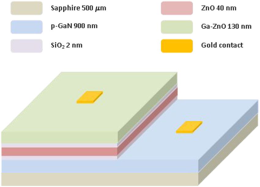
Rahman: Zinc oxide light-emitting diodes: a review

                GaN-based color LEDs;43,44 doing the same with ZnO may                            dopant solubility. Similar problems have beset numerous
                not be possible or will require further research effort.                          other efforts to prepare acceptable p-type ZnO films.
                However, most importantly, the biggest single reason for                          However, recently, Reynolds et al.57 have shown that suffi-
                the lack of progress with ZnO devices has been the inability                      ciently high nitrogen doping followed by appropriate thermal
                to create robust p-type material. The following section takes                     annealing can lead to significantly high (∼1018 cm−3 ) p-type
                a look at this continuing problem.                                                behavior in ZnO, at room temperature. Through secondary
                                                                                                  ion mass spectrometry, Raman-scattering, photolumines-
                                                                                                  cence (PL), and Hall-effect studies, they concluded that
                4 Electrical Doping of ZnO                                                        the observed p-type electrical activity is a result of doped
                Synthetic, as-grown ZnO exhibits n-type conductivity. The                         N atoms evolving from their initial incorporation on Zn
                origin of this is not definitively established yet but, princi-                   sites to a final shallow acceptor complex VZn − NO − Hþ ,
                pally, it appears to be due to a large number of native defects,                  with an ionization energy of around 130 meV. This complex,
                such as oxygen vacancies, zinc vacancies, oxygen intersti-                        they determined, is responsible for the p-type character of
                tials, and zinc interstitials.45–47 Of these, oxygen vacancies                    ZnO thus doped. It should be mentioned here that very recent
                have the lowest formation energy and are thus the easiest                         work has also reported on ferromagnetism in N-doped ZnO
                to form.48 This feature makes it difficult to induce significant                  thin films,58 which may have interesting implications for
                amount of p-type character through known doping tech-                             future magneto-optic devices.
                niques. The major remaining problem with ZnO has been                                 Further work is proceeding on finding the best route for
                the unavailability of sufficiently highly doped p-type                            p-type doping of ZnO, which is stable and reproducible.
                material. This problem is also seen with other III–V and                          An industrially acceptable method of producing p-type
                II–VI wide bandgap semiconductors—almost all of which                             regions for ZnO-based devices is still not firmly established.
                are easy to dope n-type but much harder to dope p-type.                           Nevertheless, efforts continue to investigate mechanisms
                In this respect, the only major exception appears to be                           that seem to prevent p-type doping of ZnO as well as to
                ZnTe, which is quite easy to dope p-type.49 However, to fab-                      find novel, ingenious methods for achieving device-quality
                ricate efficient bipolar devices, both n- and p-type materials                    p-ZnO material.
                are necessary. This has required a large amount of effort,
                directed toward understanding the dynamics of carrier dop-
                                                                                                  5 Heterojunction ZnO LEDs
                ing in ZnO. Over the past few years, considerable progress
                has been made in this area and now material with hole                             ZnO can be epitaxially grown on all three common substrate
                concentration in excess of 3 × 1019 cm−3 has been demon-                          materials used for making conventional blue LEDs: sap-
                strated. However, the various processes developed so far                          phire,59,60 GaN,61 and SiC.62 Indeed, ZnO growth on all
                have either suffered from lack of reproducibility, low achiev-                    of these substrates has been extensively reported in the liter-
                able hole concentration, and/or gradual diminution of p-type                      ature. This trend is easy to understand as GaN-based blue
                character over time. Undoubtedly, further advances are                            LEDs—the archetypical wide bandgap LEDs—have been
                needed in this direction so that controllably doped p-type                        conventionally made through epitaxial growth on exactly
                material of reasonably high hole concentration and mobility                       these substrates. The lattice mismatch of ZnO with each
                becomes routinely available.                                                      of these materials is given in Table 1 here. The ability to cre-
                    A good review of the general aspects of ZnO doping,                           ate such heterointerfaces has been exploited in constructing
                bandgap engineering, and associated topics has recently                           heterojunction ZnO LEDs. It should be noted here that these
                been provided by Kozuka et al.50 This review can be con-                          structures should strictly be called heteroepitaxial but the
                sulted as a starting point for understanding the contemporary                     term heterojunction, in this context, is common in the liter-
                material challenges with ZnO family materials. Most work                          ature and thus this term is used throughout in this review. As
                on developing good quality p-type ZnO begins from assump-                         mentioned before, this has been the principal way through
                tions that the difficulty in creating stable high hole concen-                    which the unavailability of good p-type ZnO has been
                tration ZnO is related to either the acceptor levels being too                    accommodated for making ZnO-based pn-junction LEDs.
                deep, compensation of native defect levels or the low solu-                       II-oxide/III-nitride heterostructures family can cover a wide
                bility of dopants.51–53 Various research groups have then                         space of interfacial lattice matches and band gaps. From
                attempted to solve each of these problems in a different way.                     MgZnO to CdZnO and from AlGaN to InGaN, a full
                    Substitution of group-I elements for Zn sites or the sub-
                stitution of group-V elements for O sites can, in principle,
                lead to p-type ZnO but studies, both theoretical and exper-                       Table 1 Material properties of some possible substrates for the
                imental, have shown that the situation for ZnO doping is                          growth of epitaxial ZnO layers.
                much more complicated than, e.g., for silicon. The relative
                sizes of substituting ions, charge compensation effects,                                                                           Lattice constant
                defect complexes, and bond strains all play important                                               Bandgap Density   Lattice       mismatch with
                roles in the case of p-type ZnO doping and make obtaining                         Substrates          (eV)  (g/cm3) constant (Å)       ZnO (%)
                good quality p-ZnO very difficult. A number of techniques,
                                                                                                  ZnO                 3.4     5.6        3.25                0
                including secondary ion mass spectroscopy,54 have been
                used for investigating the solubility, placement, and activa-                     Sapphire            9.1     4          4.76               46.5
                tion of a range of potential dopants in ZnO. Nitrogen-doped
                ZnO once appeared very promising for creating p-type ZnO                          GaN                 3.4     6.15       3.19                1.8
                epilayers,55,56 but it was found that N-doped ZnO is not                          Silicon carbide     3.0     3.2        3.10                4.6
                stable at higher temperatures and also suffers from limited

                Optical Engineering                                                       010901-5                                       January 2019   •   Vol. 58(1)

Downloaded From: https://www.spiedigitallibrary.org/journals/Optical-Engineering on 07 Sep 2021
Terms of Use: https://www.spiedigitallibrary.org/terms-of-use
Rahman: Zinc oxide light-emitting diodes: a review
range of alloy compositions are available for close across- half-maximum of about 50 nm. Cathodoluminescence
the-interface lattice matching and bandgap adjustment. (CL) studies supported the conclusion that the EL was gen-
Bulashevich et al.63,64 have analyzed the operation of erated in the GaN epilayer rather than in ZnO. The light was
ZnO/GaN heterostructures diodes through simulations. emitted when electrons injected from n-type ZnO into p-type
Their studies shed light on the mechanism of operation of GaN recombined with holes there. n-ZnO-on-p-GaN LEDs
such heterostructure LEDs and laser diodes. Among the have recently also been made through the ALD technique.69
parameters they studied were the internal quantum efficiency Compared to MBE and MOCVD processes, ALD is still a
of hybrid diodes and its dependence on operating tempera- relatively immature technology but holds great promise for
ture. A more recent review on ZnO/MgZnO heterostructures structures that require the growth of extremely thin layers
for LEDs and other optoelectronic applications has been pro- with very closely controlled stoichiometry. As ALD gets
vided by Kozuka et al.,50 where various topics ranging from developed further, it will partially replace MBE and
growth techniques and band alignments to device fabrication MOCVD for making ZnO LEDs because of its ability to pre-
and characterization have been discussed. cisely target material thickness and composition in quantum
Epitaxial heterostructure LED structures involving ZnO well-based devices.
are actually easier to grow and are more forgiving in Yet another work from Russia, also reported in the year
terms of lattice mismatch than is the case with III–V homo- 2003, described the fabrication of n-ZnO/p-AlGaN hetero-
junction LEDs.65 This is because of the ionic character of structure grown on 6H-SiC substrate.70 In this work, the
ZnO. Ionic bonds have spherical potential wells, in contrast p-AlGaN layer was grown on SiC by hydride vapor phase
to the anisotropic wells of covalently bonded semiconduc- epitaxy, whereas the n-ZnO layer was subsequently depos-
tors. This feature makes the potential energy profile ited by CVD. The use of different growth techniques for
relatively insensitive to the variation of the atomic arrange- growing the p- and n-type layers for such heterostructures
ment in ionic compounds compared with that in covalent has been a common practice. The ZnO/AlGaN heterostruc-
compounds. Thus the interface in heteroepitaxial systems tures exhibited good diode characteristics with forward
with large lattice misfits is smoothly connected in ionic mate- voltage of 3.2 V. Above this voltage, UV light with peak
rials and the formation of dangling bonds and dislocations is wavelength of 398 nm was emitted by the diode. On raising
suppressed compared with that in covalent materials. This the temperature, light emission was seen at temperatures as
structural property has led to many successful demonstra- high as 500 K. CL studies and temperature dependence of EL
tions of heterostructure ZnO LEDs. supported the conclusion that the light was emitted by exci-
tonic decay in the ZnO layer. This was one of the first dem-
onstrations of UV emission from a heterostructure ZnO LED.
5.1 ZnO-on-GaN Heterostructure LEDs Note that in this work SiC wafers were used only as the
Diodes made from n-type epitaxial ZnO overlayers grown on growth substrate—not as an electrically active material.
p-type epitaxial GaN layers have been the most studied con-
figuration for heterojunction ZnO LEDs. The reverse struc-
ture, comprising of p-type GaN overlayers deposited on 5.2 ZnO-on-SiC Heterostructure LEDs
n-type ZnO, has also been investigated but its descriptions n-type ZnO can also be directly deposited on p-type SiC to
have been less common. In the case of ZnO-on-GaN struc- form pn-junction devices. Such a material combination
tures, the GaN layer can be deposited on a variety of meta- was reported by Yuen et al.71 from the Nanyang Techno-
morphic substrates of which epitaxial GaN templates on logical University in Singapore. A remarkable feature of their
sapphire substrates are the most common. An example of this work was the low temperature (∼150°C), in which ZnO dep-
kind of work was reported by a group of Russian researchers osition was carried out. p-doped 4H-SiC wafer with hole con-
in 2003.66,67 They grew GaN layers through molecular beam centration of 1 × 1019 cm−3 and hole mobility of 120 cm2 ∕Vs
epitaxy (MBE) on a sapphire substrate where the top layer was used in this work. An overlayer of Al-doped ZnO was
was an Mg-doped p-type layer. On top of it, they deposited a deposited by filtered cathodic vacuum arc technique using
layer of Ga-doped n-type ZnO through low-pressure chemi- a ZnO target containing 3% of Al. An oxygen partial pressure
cal vapor deposition (CVD). While a variety of dopants, such of 5 × 10⁻⁴ Torr was maintained during the reactive deposi-
as Al, can be used for preparing n-type ZnO, use of Ga is tion process. LEDs were fabricated from the heterostructure
convenient in such situations as it is already present in material and exhibited emission at 385 nm.
the growth system as a component for depositing GaN. In yet another work pairing ZnO with SiC, a Korean team
Substitutional Ga atoms on Zn sites act as n-type dopants reported the fabrication of ZnO heterostructure LEDs by
with activation energy of around 50 meV.68 As an illustration depositing ZnO on a SiC substrate.72 In contrast to other sim-
of material properties typically achieved with these kinds ilar work, their approach involved using n-type 6H-SiC sub-
of growth processes, they measured room temperature strate, in which a 400-nm-thick Cu-doped, p-type ZnO layer
hole density and mobility in their p-GaN to be p ¼ was deposited by plasma-assisted MBE. This work is notable
3.5 × 1017 cm−3 and μp ¼ 10 cm2 V−1 s−1 , respectively. as one of the early attempts at using p- instead of n-type ZnO
They also found electron density and mobility in their for making heterostructures ZnO LEDs. Introduction of Cu
n-ZnO to be n ¼ 4.5 × 1018 cm−3 and μn ¼ 40 cm2 V−1 s−1 , leads to acceptor states in ZnO located at 0.17 eV below the
respectively. Diodes made from this heterostructure showed bottom of the conduction band, as the Cu atoms substitute for
distinct pn-junction diode-like characteristics with a forward Zn atoms.73
voltage of only 3 V. Electroluminescence (EL) was observed The epitaxy of ZnO with GaN can be improved by mak-
under forward bias with the intensity increasing linearly ing use of the various alloying opportunities available with
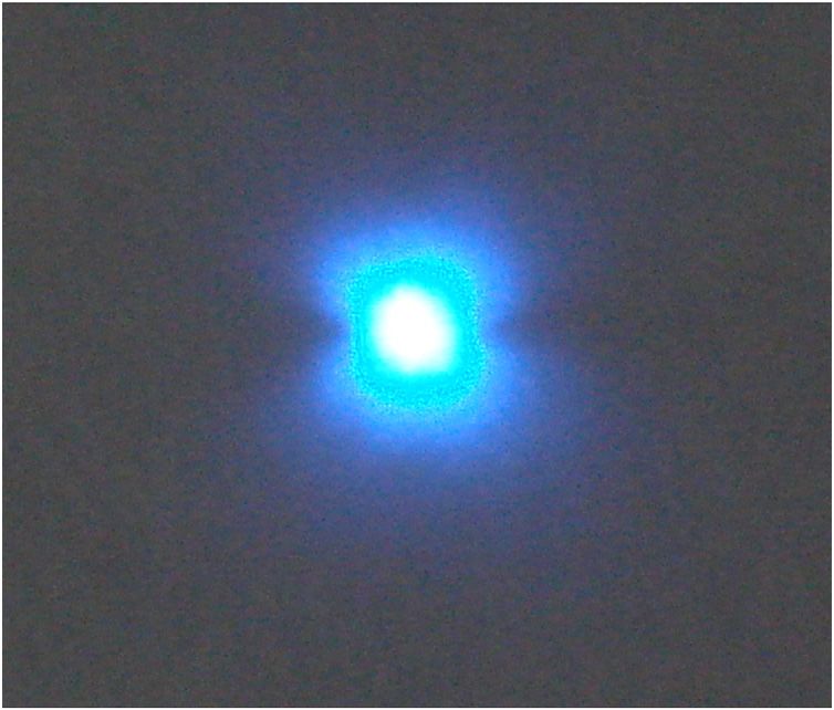
for forward currents up to 10 mA. The violet-blue light both systems. This will allow better lattice matching and
emission had a spectral peak at 430 nm with full-width at thus reduced interfacial and threading defects as well as
Optical Engineering 010901-6 January 2019 • Vol. 58(1)
Downloaded From: https://www.spiedigitallibrary.org/journals/Optical-Engineering on 07 Sep 2021
Terms of Use: https://www.spiedigitallibrary.org/terms-of-use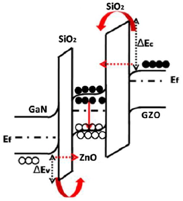
Rahman: Zinc oxide light-emitting diodes: a review

                the possibility of bandgap engineering for emission wave-                         both chemical mechanical planarization damage and chemi-
                length tuning. These considerations are even more important                       cally induced damage; leaving an atomically flat face. GaN
                for fabricating UV LEDs because they have less tolerance                          was then grown by MBE using an RF-N2 plasma source at
                for defects and other imperfections. A US-Taiwan team                             the rate of 300 nm/h. Alternatively, they also tried using
                described a UV LED structure made from n-ZnMgO/n-                                 ammonia as a source of nitrogen but found that GaN
                ZnO/p-AlGaN/p-GaN structure.74,75 They grew the entire                            grown with ammonia was always rougher than GaN grown
                structure through RF plasma-assisted MBE on c-plane                               with nitrogen. Atomic force microscopy and PL character-
                sapphire templates. LEDs of conventional design were fab-                         izations showed that high-quality GaN epilayers suitable
                ricated using both wet and dry etching processes, in keeping                      for device fabrication were achieved. Polarization control
                with the presence of both ZnO and GaN family layers in the                        of ZnO epilayers grown on GaN substrates can yield
                heterostructure. EL, associated with ZnO excitonic transi-                        high-quality UV LED material. For instance, oxygen-polar
                tions, was observed up to a temperature of 370°C. This                            ZnO films can be grown on nitrogen-polar p-GaN-on-
                work is a clear indication of the great potential inherent in                     sapphire substrates through photoassisted MOCVD. Very
                ZnO for making bright high-efficiency LEDs and even                               recently, it has been shown that this leads to the presence
                lasers operating in the blue, violet, and UV regions of the                       of a polarization-induced inversion layer at the ZnO side
                electromagnetic spectrum. In an even more recent work,                            of the heterojunction interface.82 This structure makes it pos-
                Kong et al.76 inserted a 100-nm MgZnO/ZnO/MgZnO well                              sible to obtain relatively narrow band UV emitters that emit
                between Ga-doped ZnO and Sb-doped ZnO layers. LEDs                                at 385 nm. Thus it seems that just as with GaN LEDs, ZnO
                made from this heterostructure showed strong UV EL at                             LEDs also can benefit from proper interfacial polarization
                injection currents ranging from 40 to 80 mA at room temper-                       engineering. This possibility makes the GaN-on-ZnO
                ature. The output optical power was 7.3 times that from                           scheme of particular interest for making ZnO LEDs.
                a pn-homojunction diode at the same driving current. This                             An interesting variation on the GaN/ZnO heterostructure
                demonstrates good confinement of electrons and holes in                           approach has been described by a Taiwanese team from the
                the intrinsic ZnO layer of the heterostructure.                                   National Taiwan University.83 What sets their work apart is
                                                                                                  their use of very thin SiO2 layers on either side of an
                5.3 ZnO-on-Si Heterostructure LEDs                                                undoped ZnO layer. The SiO2 -sandwiched ZnO layer was
                Although we have mainly reviewed work using sapphire,                             sitting atop an Mg-doped p-type epitaxial GaN film on
                GaN, or SiC as substrate material, there have even been                           sapphire substrate. There was a Ga-doped n-type ZnO layer
                attempts to grow ZnO on silicon substrates. Given the suc-                        deposited at the top of the device to serve as the negative
                cess in growing device-quality GaN on Si for making LEDs,                         contact (see the device structure in Fig. 4).
                this is an area where we will see more activity in the future.                        Both the SiO2 layers and the ZnO layers were deposited
                The challenges here are similar to those encountered in                           by RF magnetron sputtering. The silica layers were intended
                GaN-on-Si epitaxy. One research group has even reported                           to serve as carrier confinement layers with carriers either tun-
                optically pumped lasing from an MOCVD-grown ZnO −                                 neling through or hopping over the barriers at significant
                on − SiO2 disc laser.77 As far as LEDs are concerned,                             drive currents (see Fig. 5). The investigators noticed a sig-
                Baltakesmez et al.78 have reported on heterojunctions formed                      nificant decrease of defect-induced emission and enhance-
                by n-ZnO thin films deposited on (100) p-Si:B using an                            ment of ZnO band-edge excitonic emission, compared to
                electrochemical deposition technique. They observed broad                         devices without SiO2 barrier layers. However, their devices
                luminescence centered at the wavelengths of 390 and 510 nm                        exhibited soft turn on characteristics and a large resistance
                although the EL was not very strong. This is not surprising                       due to the presence of barrier layers.
                because the epitaxy of GaN-on-Si system is also very diffi-                           More recently, LEDs fabricated from a similar structure
                cult and if not carried out properly usually leads to material,                   through pulsed laser deposition but without silica barrier
                which is not very useful for device fabrication. However, just
                as the GaN-on-Si epitaxy has been mastered such that com-
                mercial LEDs are now available, it is conceivable that high-
                quality ZnO-on-Si material may also become available one
                day. Another yet-to-be-explored possibility is the growth of
                n-ZnO layers on commercially available GaN-on-Si wafers.
                This approach is now feasible as GaN/InGaN LEDs fabri-
                cated on GaN-on-Si wafers are now commercially available
                from companies, such as Plessey Semiconductors in the UK.

                5.4 GaN-on-ZnO Heterostructure LEDs
                While most ZnO/III-nitride heterostructures have been made
                by depositing ZnO on a nitride epilayer, growth of nitride
                on ZnO surfaces has also been investigated by several
                groups.11,79,80 One such work was described in 2004 by
                an academic–industry collaboration consisting of researchers
                from Virginia Commonwealth University and Cermet Inc.81
                Polished ZnO wafers were first annealed at 1050°C to obtain
                atomically flat surfaces suitable for MBE. Studies have                           Fig. 4 Device and layer structure of a ZnO LED with silicon dioxide
                revealed that such thermal annealing is useful for removing                       barrier layers.

                Optical Engineering                                                       010901-7                                         January 2019   •   Vol. 58(1)

Downloaded From: https://www.spiedigitallibrary.org/journals/Optical-Engineering on 07 Sep 2021
Terms of Use: https://www.spiedigitallibrary.org/terms-of-use
Rahman: Zinc oxide light-emitting diodes: a review

                                                                                                  (1-D) nanostructures.91,92 Several groups have reported fab-
                                                                                                  rication of heterostructure ZnO nanowire LED structure.
                                                                                                  Park and Yi93 described the fabrication of LEDs from
                                                                                                  ZnO nanowires grown on p-GaN surface (on sapphire)
                                                                                                  through catalyst-free MOCVD. They planarized the top of
                                                                                                  ZnO nanorods by impregnating and filling the nanorods
                                                                                                  assembly with photoresist. Ti/Au contact was deposited at
                                                                                                  the top end of ZnO nanorods to form the cathode contact,
                                                                                                  whereas Pt/Au contact was deposited on the p-GaN to
                                                                                                  form the anode contact. The diode thus formed showed
                                                                                                  no EL under forward bias but light emission was observed
                                                                                                  under reverse bias. At reverse voltages up to 4 V, only
                                                                                                  a broad yellow defect band luminescence was seen, but at
                                                                                                  voltages above 4 V a blue emission centered at 430 nm
                                                                                                  was also observed. Further increase of the reverse voltage
                Fig. 5 Band structure of a ZnO LED with silicon dioxide barrier layers.
                Reprinted with permission from Ref. 83, Optical Society of America.               to values above 6 V showed the emergence of weak UV
                                                                                                  emission. Clearly different charge injection and recombina-
                                                                                                  tion mechanisms were being activated at different threshold
                layers have also been described by a Chinese Inter-                               voltages. Impact ionization is often the mechanism that leads
                University collaboration.84                                                       to light emission in such devices. Although their device was
                    In making heterostructures LEDs where ZnO is one com-                         not a satisfactory UV-emitter, it was a forerunner to other
                ponent of the diode, materials are almost always deposited                        ZnO nanorods-devices that were developed later.
                on each other through an epitaxial process. This is essential if                      ZnO nanowire structures made further progress when the
                one wants an intimate enough interface for charge carrier                         technology to transition from 1-D to two-dimensional (2-D)
                injection. If this is not a requirement then other methods,                       growth (or vice versa) during MOCVD growth was devel-
                such as wafer bonding can be utilized. As an example of                           oped. This allows low-defect transitions between planar
                this, a wafer bonding process for making LEDs was                                 (2-D) and nanowire (1-D) layers. An example of this
                described in 2007 by a University of California at Santa                          comes from a South Korean collaboration who described
                Barbara team.85 In their work, they made use of a conven-                         pn-junction diodes made by growing ZnO nanowires on
                tional GaN/InGaN LED wafer, which was bonded to an n-                             p-GaN.94 MOCVD was used to first grow a p-GaN layer
                type hydrothermally grown bulk wafer. The bonding process                         on a sapphire substrate and then diethyl zinc + oxygen pre-
                was carried out by heating ZnO and GaN LED wafers                                 cursors were used to grow vertically aligned ZnO nanowires
                together at 700°C in a nitrogen atmosphere under 2 MPa                            on top of the GaN layer. Growth temperature was then
                pressure. Heat-and-pressure wafer bonding causes some                             altered to make a transition and grow a cap layer of planar
                material diffusion across the bonded interface so that the                        ZnO on top of the nanowire layer. Electrical contacts were
                interface becomes somewhat diffused but the bonded                                deposited on the ZnO cap layer and on the p-GaN layer
                composite wafer exhibits high mechanical strength. The                            (exposed through etching). In structures like these, the tran-
                bonded wafers were etched to form truncated hexagonal ZnO                         sition between 1-D and 2-D growth is affected by changing
                pyramids. These served to enhance light extraction from the                       the growth temperature and thus the diameter and density of
                underlying conventional GaN/InGaN LED by reducing the                             the ZnO nanorods are dependent on the substrate tempera-
                refractive index discontinuity from GaN to air. They demon-                       ture. Reactor pressure also influences growth morphology, as
                strated a highly efficient “mega-cone” LED. For instance, at                      reduced pressure promotes vertical alignment of nanorods.
                50 mA forward current, their LED was 2.6 times brighter
                                                                                                  pn-junction diodes fabricated from this material showed
                than a conventional planar GaN LED. There have been
                                                                                                  good rectifying behavior but a rather large forward voltage
                other reports86–89 of ZnO being used in this index-matching
                                                                                                  drop of around 11 V and no light emission was reported. This
                role with GaN LEDs, especially because it can be doped
                                                                                                  was attributed to interface defects and insufficient ohmic
                n-type easily and can thus serve as the n-type contact to
                                                                                                  contact area. This observation underscores the fact that
                the LED.
                                                                                                  exquisite morphology control is essential for growing struc-
                                                                                                  tures where a dimensional transition takes place. As this is
                5.5 ZnO Nanowire Heterostructure LEDs                                             difficult to do in a research setting, let alone in a manufac-
                So far, we have looked at heterostructure ZnO LEDs employ-                        turing environment, devices with such structures are unlikely
                ing planar ZnO films. Due to its morphology and growth                            to be commercialized any time soon.
                characteristics, ZnO lends itself, under suitable conditions,                         The growth of ZnO nanowires has rapidly advanced dur-
                to columnar growth, forming ZnO nanowires.90 MBE,                                 ing the past decade so that higher quality material can now be
                MOCVD, or hydrothermal growth can be used to grow                                 grown.95 Due to these developments, several groups have
                ZnO nanowires. Semiconductor nanowires have attracted                             now succeeded in developing light-emitting pn-junction
                increasing attention in recent years for making light-emitting                    diodes from the p-GaN/n-ZnO nanowire system. One such
                devices. When used in LEDs, nanoscale columnar morphol-                           work has been described by Zhang et al.96 They grew uni-
                ogy offers several advantages over planar films. These                            form arrays of 100 to 150 nm diameter, ∼5-μm long, n-type
                include increased junction area, reduced temperature sensi-                       ZnO wires on p-GaN-on-sapphire substrates through a
                tivity, enhanced polarization dependence of reflectivity,                         physical vapor deposition process.97,98 Their nanowires grew
                and improved carrier confinement in one-dimensional                               abruptly on the GaN surface without any planar ZnO layer

                Optical Engineering                                                       010901-8                                      January 2019   •   Vol. 58(1)

Downloaded From: https://www.spiedigitallibrary.org/journals/Optical-Engineering on 07 Sep 2021
Terms of Use: https://www.spiedigitallibrary.org/terms-of-use
Rahman: Zinc oxide light-emitting diodes: a review
first forming on GaN. This resulted in an abrupt pn-junction been widely investigated for making GaN LEDs. In a recent
at the GaN/ZnO nanowire interface. Weak EL was observed work, reported by researchers from Henan University in
under a forward bias higher than 10 V. On increasing the China, a ZnO heterojunction LED, entirely comprised of
forward voltage, the emission intensity was seen to increase single nanowires with both p- and n-type regions, was
and shift to shorter wavelengths. In the range of 10 to 35 V, described.103 First, CVD was carried out on Si(010) substrate
the peak emission wavelength changed from blue (440 nm) to grow vertically aligned p-type AlGaN nanowires.104,105
to deep violet (400 nm). The authors proposed an interfacial These nanowires had diameters of 100 to 500 nm and
band bending model to explain this observed blue shift of the their lengths were in the range of 0.8 to 1.5 μm. Using
EL spectrum. This model suggests that electrons from ZnO another chemical vapor mediated process, extensions of
get injected into GaN where they recombine with holes to n-type ZnO were grown as continuation of these nanowires.
produce emission at the bandgap of GaN, whereas holes High resolution transmission electron microscopy showed
from GaN get injected into ZnO, producing emission corre- that the AlGaN/ZnO interfaces were very sharp and uniform
sponding to the bandgap of ZnO. These emissions, combined with a transition region of no more than 1 nm along the wire.
with interfacial recombination emission, lead to broadening Thus each nanowire was essentially a single-crystal pn-
of the emission spectrum. heterojunction. Au/Ti bilayer metal contacts were made to
In a similar work, reported by Lai et al.99 from UC the AlGaN and ZnO ends of nanowires. Current–voltage
Berkley, California, ZnO nanowire arrays grown on p- characterization showed very good rectifying behavior with
type GaN epitaxial film through a simple low-temperatureRahman: Zinc oxide light-emitting diodes: a review
While n-type ZnO nanowires can be paired with planar or
nanowire p-type GaN for making heterostructures LEDs,
another promising route employs p-type conducting organic
polymers for this purpose. This approach is feasible because
most conducting polymers show p-type conductivity and
can be easily deposited through dip- or spin-coating
techniques.112 Furthermore, a large body of work exists
on organic LEDs (OLEDs) from which appropriate polymer
materials can be chosen for fabricating hybrid organic–inor-
ganic ZnO-based LEDs. Many organic conductors, semicon-
ductors, and light-emitting materials are commercially
available from companies such as Merck and American Dye
Source. One of the early reports on making hybrid organic–
inorganic LEDs using ZnO was the work reported by
Könenkamp et al.113,114 from Portland State University.
An interesting feature of their work is that they deposited
Fig. 6 Device structure of a double heterostructure ZnO nanorod ZnO nanowires on an electrically conducting, fluorine-
LED. doped, SnO2 -coated glass substrate using an aqueous
solution electrodeposition process.115 n-type doping of the
nanowires was performed in situ by adding AlCl3 to the
white.108 Thus a prominent benefit of a double heterostruc- solution.116 This type of process is especially suitable for
ture appears to be the reduction of background emission in depositing uniform nanowire layers on large area substrates.
ZnO nanorods LEDs. After growth, the nanowires were encapsulated in polysty-
In addition to serving as a heterostructure component, rene and topped by a layer of conductive poly(3,4-ethyl-
MgZnO can also be coated on ZnO nanowires in order to ene-dioxythiophene)-poly(styrene-sulfonate) (PEDOT/PSS)
passivate them from environmental influence. Through polymer film. A gold contact was deposited at the top of
aging studies, supported by x-ray photoelectron spectros- the structure to serve as the anode of the heterostructure
copy (XPS), it has been shown that such a coating is LED. On powering up their device, the investigators
beneficial toward the longevity of ZnO nanowire LEDs.109 observed white EL at a current density of 5 mA∕cm2 (cor-
This comes about because surface-adsorbed O2 and OH− responding to 100 mA∕cm2 at the nanowire tips). The EL
species on bare ZnO nanowires act as acceptor and donor spectrum consisted of a broad defect-related luminescence
surface states and effectively quench UV EL. Producing band centered at 620 nm and a weak excitonic peak from
a ZnO/MgZnO core/shell structure avoids such deleterious recombination in ZnO nanowires at 360 nm. This work
adsorption, thus maintaining UV emission and increasing clearly showed the need for further progress, both in improv-
the longevity of ZnO nanowire LEDs. Surface passivation ing the electrical characteristics of the device and in strength-
of reduced dimensionality structures, such as nanowires ening the excitonic emission. Workers from the same
and quantum dots, is essential for prolonging the operating laboratory later extended their research by depositing ZnO
lifetime of devices that employ these structures. This is, thus, nanowires on flexible ITO-coated polymer substrates.117
a complication that has to be addressed in order to get the This led to a highly flexible ZnO nanowire LED that emitted
benefits that reduced dimension semiconductor structures broadband light under forward bias. It should be noted here
confer on functional devices. While this may appear to that by combining ZnO nanowires with organic electronic
take some attention away from the main structure of the materials, flexible light-emitting devices can be constructed.
LED, which is responsible for light emission, its importance Such devices can find many applications in fields ranging
should never be underestimated. This is because surface from on-person devices to health care and environmental
recombination and associated effects can both reduce radia- monitoring.
tive recombination efficiency and lead to irreversible deterio- Yet another example of organic polymer/ZnO nanowire
ration (aging) of the device. LED was described by an international research collabora-
In a very recent work reported by a US-China team, Gao tion in 2006.118 This group utilized a layer structure consist-
et al.110 have described the fabrication and operation of ZnO ing of n-type ZnO nanowires grown on an n-type rather
nanowire Schottky LEDs. They made their devices by depos- than p-type GaN substrate. They filled their nanowire layer
iting gold at the top ends of ZnO nanowire arrays. These with the hole-conducting PEDOT/PSS polymer. A top ITO
devices exhibited clear rectifying characteristics and, at contact was deposited as the anode while the n-type GaN
high forward bias currents, excitonic luminescence centered substrate was used as the cathode of the diode. Electrical
at 380 nm. The UV radiation intensity increased with further characterization revealed that the device had a soft I − V
increase in drive current. This characteristic clearly showed curve. The EL spectrum exhibited several peaks throughout
an excitonic UV LED operation and demonstrated that ZnO the visible region, the near-IR, and the near-UV. The near-
Schottky devices are a strong contender for making UV UV peak originated from band-edge recombination in ZnO
LEDs. It should be noted that a simpler planar metal–insu- nanowires, whereas the other peaks came from defect states
lator–semiconductor ZnO diode employing HfO2 insulator in the nanowires and at the GaN–ZnO nanowire interface.
was already reported back in 2009 by the Chinese team Co-occurrence of band-edge EL with broad defect band
of Huang et al.111 Their device emitted 370-nm radiation luminescence is a feature that is often observed in hetero-
at a voltage as low as 2 V. structure ZnO LEDs.119 Sometimes, it leads to the light
Optical Engineering 010901-10 January 2019 • Vol. 58(1)
Downloaded From: https://www.spiedigitallibrary.org/journals/Optical-Engineering on 07 Sep 2021
Terms of Use: https://www.spiedigitallibrary.org/terms-of-useYou can also read