DHAN-T Module DECT ULE Platform - Datasheet - DSP Group
←
→
Page content transcription
If your browser does not render page correctly, please read the page content below
DHAN-T Module
DECT ULE Platform

   Datasheet

     Version 2.5

       April 2021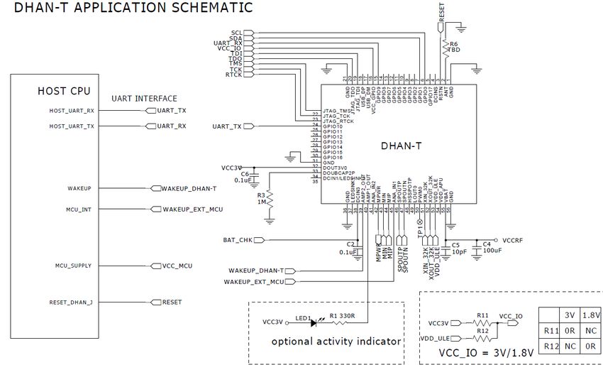
Version 2.5                                         DHAN-T DECT ULE Module                                                                 Disclaimer

  This document is provided by DSP Group, Inc. and/or one or more of its subsidiaries (“DSP Group”). All information and data
  contained in this document is for informational purposes only, without any commitment on the part of DSP Group, and is not to
  be considered as an offer for a contract. DSP Group shall not be liable, in any event, for any claims for damages or any other
  remedy in any jurisdiction whatsoever, whether in an action in contract, tort (including negligence and strict liability) or any other
  theory of liability, whether in law or equity including, without limitation, claims for damages or any other remedy in whatever
  jurisdiction, and shall not assume responsibility for patent infringements or other rights to third parties, arising out of or in
  connection with this document. Further, DSP Group reserves the right to revise this publication and to make changes to its content,
  at any time, without obligation to notify any person or entity of such revision changes. These materials are copyrighted and any
  unauthorized use of these materials may violate copyright, trademark, and other laws. Therefore, no part of this publication may
  be reproduced, photocopied, stored on a retrieval system, or transmitted without the express written consent of DSP Group. Any
  new issue of this document invalidates previous issues.
  DSP Group reserves the right to revise this publication and to make changes to its content, at any time, without obligation to notify
  any person or entity of such revision changes.
  © 2021 DSP Group Confidential. All rights reserved.
  For DSP Group worldwide sites and related contact information, see http://www.dspg.com/corporate/offices

April 2021                                            DSP Group Confidential                                                                    2/19
Version 2.5                                                       DHAN-T DECT ULE Module                                                                Table of Contents

                                                     TABLE OF CONTENTS
1     INTRODUCTION ........................................................................................................................................... 4
    1.1      General Description ................................................................................................................................. 4
    1.2      Features .................................................................................................................................................... 4
    1.3      Block Diagram ......................................................................................................................................... 4
2     PIN AND SIGNAL DESCRIPTION............................................................................................................... 5
3     ELECTRICAL SPECIFICATIONS ................................................................................................................ 8
    3.1      Absolute Maximum Ratings .................................................................................................................... 8
    3.2      Recommended Operating Conditions ...................................................................................................... 8
    3.3      Peak and Hibernation Currents ................................................................................................................ 8
    3.4      Transmitter............................................................................................................................................... 9
    3.5      Receiver ................................................................................................................................................... 9
4     APPLICATION REFERENCE SCHEMATIC ............................................................................................. 10
5     INTERFACING DHAN-T WITH EXTERNAL MCU ................................................................................. 11
    5.1      RSTN Input............................................................................................................................................ 11
    5.2      UART, SPI Interfaces ............................................................................................................................ 11
6     APPLICATION PCB DESIGN RECOMMENDATIONS............................................................................ 12
7     ASSEMBLY INFORMATION ..................................................................................................................... 13
    7.1      Mechanical Drawing .............................................................................................................................. 13
    7.2      PCB Footprint Detail ............................................................................................................................. 13
    7.3      Pick & Place, Reflow ............................................................................................................................. 14
8     SUPPLEMENTARY INFORMATION ........................................................................................................ 15
    8.1      Labeling ................................................................................................................................................. 15
    8.2      Handling Guidance ................................................................................................................................ 15
    8.3      FCC and IC Interference Statement ....................................................................................................... 16
    8.4      Declaration of Conformance (DoC)....................................................................................................... 16
    8.5      IPEI and EMC ....................................................................................................................................... 16
    8.6      Ordering Information ............................................................................................................................. 17
    8.7      Change Log............................................................................................................................................ 17

April 2021                                                          DSP Group Confidential                                                                                     3/19
Version 2.5 DHAN-T DECT ULE Module Introduction
1 Introduction
1.1 General Description
DSP Group’s DHAN-T module is based on the state-of-the-art DHX101, a 4th generation DECT System on a
Chip (SoC). The DHAN-T module is well suited for all DECT and ULE device applications. The DHAN-T
software stack includes standard DECT ULE MAC-PHY connectivity as well as HAN-FUN (ULE Alliance
standard) functionality for Dual-Mode (data and audio) ULE. The application software written by the customer
typically runs atop the communication stack running on the DHX101 within the DHAN-T. However, the
application Host can also run on an external MCU that communicates with the DHAN-T via a UART interface.
1.2 Features
• Excellent radio performance, with over 119dB system gain
• Includes a printed antenna
• Radio covers all regional DECT bands with a simple re-configuration of the EEPROM
• Fully compliant with ETSI DECT and ULE standards, awarded CE, FCC and IC certification
• Compact dimensions: 27.2x16.9x3.3mm (including the RF shield height)
• Minimized external BOM
• Operating temperature: -40ºC to 85ºC
1.3 Block Diagram
DHAN-T
QSPI
DHX101-88pin
13.824M
13.824M
RF
Matching
/Filter I2C, UART, SPI, JTAG, TDM
32.768K
32.768K
Figure 1-1: DHX101 DHAN-T Module Block Diagram
April 2021 DSP Group Confidential 4/19Version 2.5 DHAN-T DECT ULE Module Pin and Signal Description
2 Pin and Signal Description
See Figure 2-1 and Table 2-1 for detailed pin diagram and description.
Figure 2-1: DHAN-T Module Pin Diagram
Table 2-1: DHAN-T Module Pin Description
PIN NO. NAME DESCRIPTION/TYPE
1 GND GND
2 ANT Diversity antenna. Leave not connected (NC)
For standalone operation, shunt this pin to GND with
100nF. For an application running on an external
3 RSTN
MCU, this pin should be connected to a Host MCU
IO and used to reset the DHAN-T
4 DCINS Leave NC
April 2021 DSP Group Confidential 5/19Version 2.5 DHAN-T DECT ULE Module Pin and Signal Description
PIN NO. NAME DESCRIPTION/TYPE
5 GPIO17
GPIO or I2C Clock. Open Drain, reset value is
6 SCL (GPIO0)
floating. Leave NC if not used.
GPIO or I2C Data. Open Drain, reset value is
7 SDA (GPIO1)
floating. Leave NC if not used.
8 GPIO2 GPIO or TDM_TXD
9 GPI03 GPIO or TDM_RXD
10 GPIO4 GPIO or TDM_FSYNC
11 GPIO5 GPIO or TDM_FSYNC
12 GPIO6 GPIO or SPI Data In. Leave NC if not used
13 GPIO7 GPIO or SPI Data Out. Leave NC if not used
14 GPIO8 GPIO or SPI Clock
15 GPIO9 GPIO or UART Rx or SPI Chip Select
Input. Sets the IO Logic level at the module
16 VCC_GPIO
interface at 1.8 or 3V.
17 USB_DM
18 USB_DP
19 TDI JTAG Data In. Connect to TP
20 TDO JTAG Data Out. Connect to TP
21 GND
22 TMS JTAG Mode Select. Connect to TP
23 TCK JTAG Clock. Connect to TP
24 RTCK JTAG Reset. Connect to TP
25 GPIO10 GPIO or UART Tx
26 GPIO11 GPIO
27 GPIO12 GPIO
28 GPIO13 GPIO
29 GPIO14 GPIO
30 GPIO15 GPIO
31 GPIO16 GPIO
32 GND
33 DOUT3V0 3V (Doubler) Output. While DHAN-T is
hibernating, this pin is either in tristate (default SW
configuration) or pulled to GND. Can be used in
conjunction with GPIO7 and 8 above to drive a
LED or button during non-hibernation modes
34 DOUBCAP2P Pull down with 1M resistor
35 LEDSINK2/DCIN1 ULE I/O. Leave NC if not used
36 GND GND
April 2021 DSP Group Confidential 6/19Version 2.5 DHAN-T DECT ULE Module Pin and Signal Description
PIN NO. NAME DESCRIPTION/TYPE
37 LEDSINK1/PWM
38 DCIN3 ADC input used to monitor power supply input
ULE I/O. Typically used (as input) to wake up the
39 AMP2_OUT
DHAN-T from hibernation
ULE I/O. Typically used (as output) to indicate
40 AMP1_OUT
DHAN-T is active (logic high)
ULE I/O. During hibernate, Logic High should not
41 ANA2_IN be applied to this pin (it can result in leakage
current). Leave NC if not used
42 MPWR Microphone Power
43 MIN Leave NC if not used
44 MIP Leave NC if not used
45 ANA_IN1 ULE I/O. Leave NC if not used
46 SPOUTP Speaker Output, Positive
47 SPOUTN Speaker Output, Negative
48 HSSPOTP Headset Speaker Out, Positive
49 LOUT Headset Speaker Out, Negative
50 PWM0 Analog Output
51 XIN_32K Connect to 32.768 XTAL
52 XOUT_32K Connect to 32.768 XTAL
1.8V output. Active during hibernate. Can be used
53 VDD_ULE
to power VCC_GPIO (Pin16)
54 VDD_APU 1.8V Test Point. Leave NC
Power Supply Input. Connect to battery or regulated
55 VBAT
3V supply
56 GND GND
April 2021 DSP Group Confidential 7/19Version 2.5 DHAN-T DECT ULE Module Electrical Specifications
3 Electrical Specifications
Unless otherwise noted, all specifications are for 25ºC.
3.1 Absolute Maximum Ratings
Minimum voltage applied to all pins: -0.3V
Maximum voltage applied to all pins: +4.6V
Storage temperature range: -45 to +90ºC
Note: Functionality at or above these limits is not implied. Exposure to absolute maximum ratings for extended
periods may affect device reliability.
3.2 Recommended Operating Conditions
Table 3-1: Recommended Operating Conditions
RATING CONDITIONS MIN TYP MAX UNIT
Operating ambient -40 +25 +85 °C
temperature
VBAT 1.95 3.0 3.6 V
All GPIOs VIL 0.8 V
Condition: VIH 2.0
VCC_GPIO is 3V VOL 0.4
VOH 2.4
All GPIOs VIL 0.63 V
Condition: VIH 1.17
VCC_GPIO is VOL 0.45
1.8V VOH 1.35
RSTN VIL 0.3*VBAT V
VIH 0.6*VBAT
DCIN3 1.95 3.0 VBAT V
3.3 Peak and Hibernation Currents
VBAT=3V
Table 3-2: Peak and Hibernation Currents
PARAMETER TEST CONDITIONS TYP MAX UNIT
Tx Current Band=EU @ 23dBm 400 480 mA
Tx Current Band=US @ 21dBm 250 300 mA
Rx Current Max Gain Setting 125 135 mA
April 2021 DSP Group Confidential 8/19Version 2.5 DHAN-T DECT ULE Module Electrical Specifications
PARAMETER TEST CONDITIONS TYP MAX UNIT
Paging Current 1s response latency 90 µA
Hibernation 2 µA
Current
3.4 Transmitter
VBAT=3V
Table 3-3: Tx Characteristics
CHARACTERISTICS TEST CONDITIONS MIN TYP MAX UNIT
NTP Band=EU 21.5 23 24 dBm
NTP Band=US 19 20 21 dBm
Harmonics Band=EU & US -40 -35 dBm
Transmission Mask EN 301406 Comply N/A
Paragraph 5.3.3
Frequency Offset EN 301406 -50 8 +50 KHz
Paragraph 5.3.1
Frequency Drift EN 301406 -15 0 +15 KHz/Slot
Paragraph 5.3.5
Emission Due EN 301406 dBm
Modulation Paragraph 5.3.6.2
M±1 -20 -8
M±2 -42 -30
M±3 -47 -40
M>±3 -50 -44
3.5 Receiver
VBAT=3V
Table 3-4: Rx Characteristics
CHARACTERISTICS TEST CONDITIONS MIN TYP MAX UNIT
Sensitivity, BER < EU Band -96 -93 dBm
1000ppm
Maximum input power EU Band 15 dBm
April 2021 DSP Group Confidential 9/19Version 2.5 DHAN-T DECT ULE Module Application Reference Schematic
4 Application Reference Schematic
Figure 4-1: DHAN-T Reference Schematic
April 2021 DSP Group Confidential 10/19Version 2.5 DHAN-T DECT ULE Module Interfacing DHAN-T with External MCU
5 Interfacing DHAN-T with External MCU
5.1 RSTN Input
At power-up, the Application Host on the external MCU should hold pin 3 (RSTN Input) at logic Low until it
is ready to establish communication (via UART) with the DHAN-T. When ready, the Application Host should
apply a rising edge (and leave at Logic High) and wait for the “Hello” indication from the DHAN-T. If at some
point later on the MCU cannot communicate with the DHAN-T, it should apply a low going pulse of >100uS
to reset the DHX101 on the DHAN-T. Note that the RSTN pin is powered by the VBAT power domain. The
minimum Logic High level is 0.6*VBAT.
5.2 UART, SPI Interfaces
Applications requiring a UART I/F and an SPI interface (eg, SmartVoice ULE applications), map the former to
GPIOs 10 and 11 (Rx, Tx respectively) and the latter to GPIOs 6-9. Where only the UART I/F is required (as
in the Reference Schematic provided in section 4), UART Rx is assigned to GPIO9 and Tx to GPIO10.
April 2021 DSP Group Confidential 11/19Version 2.5 DHAN-T DECT ULE Module Application PCB Design Recommendations
6 Application PCB Design Recommendations
It is recommended that unused pads on the Application PCB not be left as isolated islands of copper but rather
be anchored via inner layers of the PCB. It is also recommend that GND vias be applied liberally in the vicinity
of GND pins 1, 21, 36 and 56.
The following layout recommendations for embedding the DHAN-T on the Application board:
1. Implement a solid ground under the DHAN-T module.
2. Do not route signal traces under the module. Use the bottom layer for signal routing.
3. Locate the antenna on the edge of the PCB.
4. Release from GND on all layers under the DHAN-T antenna.
See Figure 6-1 for recommended design details.
Figure 6-1: Application PCB Design
April 2021 DSP Group Confidential 12/19Version 2.5 DHAN-T DECT ULE Module Assembly Information
7 Assembly Information
7.1 Mechanical Drawing
+/-10%
15.3mm
+/- 1mm
Shield Width
7.2 PCB Footprint Detail
April 2021 DSP Group Confidential 13/19Version 2.5 DHAN-T DECT ULE Module Assembly Information
7.3 Pick & Place, Reflow
The DHAN-T module uses a flat shield cover to facilitate a fully automatic assembly process. For backing and
reflow recommendations, use MSL 3 in the JEDEC/IPC standard J-STD-20b. The temperature classification
(TC) for the module is 245° C.
April 2021 DSP Group Confidential 14/19Version 2.5 DHAN-T DECT ULE Module Supplementary Information
8 Supplementary Information
8.1 Labeling
See Figure 8-1 for labeling details. The label is attached to the module shield.
Figure 8-1: DHAN-T Module Labeling Details
8.2 Handling Guidance
This module includes highly sensitive electronic circuity. Handling without proper ESD protection may damage
the module permanently.
April 2021 DSP Group Confidential 15/19Version 2.5 DHAN-T DECT ULE Module Supplementary Information
8.3 FCC and IC Interference Statement
This device complies with part 15 of the FCC rules and RSS-247 of Industry Canada. Operation is subject to
the following two conditions: (1) this device may not cause harmful interference, and (2) this device must accept
any interference received, including interference that may cause undesired operation.
Le présent appareil est conforme aux CNR d'Industrie Canada applicables aux appareils radio exempts de
licence. L'exploitation est autorisée aux deux conditions suivantes : (1) l'appareil ne doit pas produire de
brouillage, et (2) l'utilisateur de l'appareil doit accepter tout brouillage radioélectrique subi, même si le
brouillage est susceptible d'en compromettre le fonctionnement.
This Class B digital apparatus complies with Canadian ICES-003.
Cet appareil numérique de la classe B est conforme à la norme NMB-003 du Canada.
NOTE: The manufacturer is not responsible for any radio or TV interference caused by unauthorized
modifications to this equipment. Such modifications could void the user’s authority to operate the equipment.
NOTE: This equipment has been tested and found to comply with the limits for a Class B digital device,
pursuant to part 15 of the FCC Rules. These limits are designed to provide reasonable protection against
harmful interference in a residential installation. This equipment generates uses and can radiate radio frequency
energy and, if not installed and used in accordance with the instructions, may cause harmful interference to
radio communications. However, there is no guarantee that interference will not occur in a particular
installation. If this equipment does cause harmful interference to radio or television reception, which can be
determined by turning the equipment off and on, the user is encouraged to try to correct the interference by one
or more of the following measures:
• Reorient or relocate the receiving antenna.
• Increase the separation between the equipment and receiver.
• Connect the equipment into an outlet on a circuit different from that to which the receiver is connected.
• Consult the dealer or an experienced radio/TV technician for help
• This device and its antenna(s) must not be co-located or operating in conjunction with any other antenna or
transmitter
8.4 Declaration of Conformance (DoC)
DSP Group declares that the radio equipment type DHAN-T is in compliance with Directive 2014/53/EU.
The full text of the EU Declaration of Conformity is available at the Internet address www.dspg.com.
8.5 IPEI and EMC
Each DHAN-T nodule is shipped to the customer with a unique IPEI, which serves as its DECT identity.
DHAN-T will ship with an “EMC” of 0xFEB. This is the DSP Group “generic” EMC. The EMC setting
identifies a Device as belonging to a specific group of ULE Devices/Hubs that utilize some proprietary
signaling.
In either case, the customer is free to re-program these parameters.
April 2021 DSP Group Confidential 16/19Version 2.5 DHAN-T DECT ULE Module Supplementary Information
8.6 Ordering Information
Part #: DHX101MDMDFDB0AMI
8.7 Change Log
Table 8-1: List of Changes
REVISION DATE DESCRIPTION
1.1 June 4, 2018 Baseline release
1.2 August 8, Updated PCB files
2018
2.0 May 27, *Account for migration to DHX101, FW D (Part #, Block Diagram, paging
2019 idle current drain)
*Clarifications to, VCC_IO RSTN (pinout description, drive by external
MCU)
*Clarifications to TDM, SPI mapping to GPIO
*Added Reference Schematics
2.1 June 3, 2019 *Added detail PCB footprint drawing
2.2 April 16, *Clarified in Module Description that dimensions given are for the module
2020 itself, not the PCB footprint recommended for mounting the module
*Replaced pinout diagram with more legible pin labels
*Corrected JTAG TDO and TMS pin numbering in the tabulation. Now
matches the diagram
*Added labeling description
*Added tolerances to shield height and PCB thickness dimensions
2.3 January 13, *Added FCC & IC Interference Statement, Declaration of Conformance
2021 (DoC)
*Updated part #
2.4 March 4, *Added battery input to ADC in reference schematic
2021 *Noted that module was awarded regulatory certification
2.5 April 6, *Updated document styles and numbering
2021
*Added List of Figures and List of Tables
April 2021 DSP Group Confidential 17/19Version 2.5 DHAN-T DECT ULE Module List of Figures
LIST OF FIGURES
Figure 1-1: DHX101 DHAN-T Module Block Diagram ........................................................................................ 4
Figure 2-1: DHAN-T Module Pin Diagram ........................................................................................................... 5
Figure 4-1: DHAN-T Reference Schematic ......................................................................................................... 10
Figure 6-1: Application PCB Design .................................................................................................................... 12
Figure 8-1: DHAN-T Module Labeling Details ................................................................................................... 15
April 2021 DSP Group Confidential 18/19Version 2.5 DHAN-T DECT ULE Module List of Tables
LIST OF TABLES
Table 2-1: DHAN-T Module Pin Description ........................................................................................................ 5
Table 3-1: Recommended Operating Conditions ................................................................................................... 8
Table 3-2: Peak and Hibernation Currents ............................................................................................................. 8
Table 3-3: Tx Characteristics ................................................................................................................................. 9
Table 3-4: Rx Characteristics ................................................................................................................................. 9
Table 8-1: List of Changes .................................................................................................................................. 17
April 2021 DSP Group Confidential 19/19You can also read