EXPLORING DYE-SENSITIZED MESOPOROUS NIO PHOTOCATHODES - DIVA PORTAL
←
→
Page content transcription
If your browser does not render page correctly, please read the page content below
Digital Comprehensive Summaries of Uppsala Dissertations
                from the Faculty of Science and Technology 1896

                Exploring Dye-Sensitized
                Mesoporous NiO Photocathodes
                from Mechanism to Applications

                LEI TIAN

    ACTA
UNIVERSITATIS
 UPSALIENSIS    ISSN 1651-6214
                ISBN 978-91-513-0852-4
  UPPSALA       urn:nbn:se:uu:diva-402415
    2020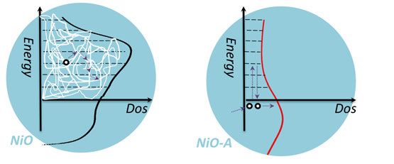
Dissertation presented at Uppsala University to be publicly examined in Häggsalen,
Ångströmlaboratoriet, Lägerhyddsvägen 1, Uppsala, Tuesday, 3 March 2020 at 09:15 for
the degree of Doctor of Philosophy. The examination will be conducted in English. Faculty
examiner: Professor Fabrice Odobel (University of Nantes).

Abstract
Tian, L. 2020. Exploring Dye-Sensitized Mesoporous NiO Photocathodes. from Mechanism
to Applications. Digital Comprehensive Summaries of Uppsala Dissertations from the
Faculty of Science and Technology 1896. 73 pp. Uppsala: Acta Universitatis Upsaliensis.
ISBN 978-91-513-0852-4.

Increasing attention has been paid on solar energy conversion since the abundant solar energy
possesses the potential to solve the problems on energy crisis and climate change. Dye-sensitized
mesoporous NiO film was developed as one of the attractive photocathodes to fabricate p-type
dye-sensitized solar cells (p-DSCs) and dye-sensitized photoelectrosynthetic cells (p-DSPECs)
for electricity and chemical fuels generation, respectively. In this thesis, we designed a well-
structured NiO-dye-TiO2 configuration by an atomic layer deposition (ALD) technique, with an
organic dye PB6 as the photosensitizer. From kinetic studies of charge separation, ultrafast hole
injection (< 200 fs) was observed from the excited state of PB6 dye into the valence band of
NiO; dye regeneration (electron injection) was in t1/2 ≤ 500 fs, which is the fastest reported in any
DSCs. On the basis of NiO-dye-TiO2 configuration, we successfully fabricated solid-state p-type
DSCs (p-ssDSCs). Insertion of an Al2O3 layer was adopted to reduce charge recombination, i.e.
NiO-dye-Al2O3-TiO2. Theoretically, such a configuration is possible to maintain efficient charge
separation and depressed charge recombination. Based on NiO-dye-Al2O3-TiO2 configuration,
the open-circuit voltage was improved to 0.48 V. Replacing electron conductor TiO2 with ZnO,
short-circuit current density was increased to 680 μA·cm-2. The photocatalytic current density
for H2 evolution was improve to 100 μA·cm-2 with a near unity of Faraday efficiency in p-
DSPECs.
   However, to further improve the performance of p-DSCs is very challenging. In p-ssDSCs,
the limitation was confirmed from the poor electronically connection of the electron conductor
(TiO2 or ZnO) inside the NiO-dye films. We further investigated the electronic property of
surface states on mesoporous NiO film. We found that the surface sates, not the bulk, on NiO
determined the conductivity of the mesoporous NiO films. The dye regeneration in liquid p-
DSCs with I-/I3- as redox couples was significantly affected by surface states. A more complete
mechanism is suggested to understand a particular hole transport behavior reported in p-
DSCs, where hole transport time is independent on light intensity. The independence of charge
transport is ascribed to the percolation effect in the hole hopping on the surface states.

Keywords: NiO, p-type, dye-sensitized solar cells, solid state, charge separation, charge
recombination, charge diffusion, transport time, surface states, electron conductor, dye
regeneration

Lei Tian, Department of Chemistry - Ångström, Physical Chemistry, Box 523, Uppsala
University, SE-75120 Uppsala, Sweden.

© Lei Tian 2020

ISSN 1651-6214
ISBN 978-91-513-0852-4
urn:nbn:se:uu:diva-402415 (http://urn.kb.se/resolve?urn=urn:nbn:se:uu:diva-402415)
To my family and friends
List of Papers

This thesis is based on the following papers, which are referred to in the text
by their Roman numerals.

      I      Tian, L.*; Föhlinger, J.*; Pati, P. B.; Zhang, Z.; Lin, J.; Yang,
             W.; Johansson, M.; Kubart, T.; Sun, J.; Boschloo, G.;
             Hammarström, L.; Tian, H. Ultrafast dye regeneration in a
             core–shell NiO–dye–TiO2 mesoporous film. Physical Chemistry
             Chemical Physics 2017, 20, 36-40.

      II     Tian, L.; Föhlinger, J.; Zhang, Z.; Pati, P. B.; Lin, J.; Kubart, T.;
             Hua, Y.; Sun, J.; Kloo, L.; Boschloo, G.; Hammarström, L.;
             Tian, H. Solid state p-type dye-sensitized NiO–dye–TiO2 core–
             shell solar cells. Chemical communications 2018, 54, 3739-
             3742.

      III    Xu, B.*; Tian, L.*; Etman, A. S.; Sun, J.; Tian, H. Solution-
             processed mesoporous NiO-dye-ZnO photocathodes: Toward
             efficient and stable solid-state p-type dye-sensitized solar cells
             and dye-sensitized photoelectronsynthetic cells. Nano Energy
             2019, 55, 59-64.

      IV     Tian, L.; Törndahl, T.; Lin, J.; Pati, P. B.; Zhang, Z.; Kubart,
             T.; Hao, Y.; Sun, J.; Boschloo, G.; Tian, H. Mechanistic
             Insights into Solid-State p-Type Dye-Sensitized Solar Cells.
             The Journal of Physical Chemistry C 2019, 123, 26151-26160.

      V      Tian, L.; Tyburski, R.; Wen, C.; Sun, R.; Huang, J.; D'Amario,
             L.; Boschloo, G.; Hammarström, L.; Tian, H. Rethinking the
             function of surface states on mesoporous NiO films, Manuscript.

*The authors contributed equally to the work. Reprints were made with per-
mission from the respective publishers.
My contributions to the included papers
I Performed the experimental work except for the synthesis of the
dye, fs-TAS and TEM. Participated in data analysis and wrote
the 1st draft of the manuscript.
II Performed most of the experimental work and data analysis.
Wrote part of the manuscript.
III Performed the experimental work on H2 evolution part, materi-
als characterization, and corresponding data analysis. Wrote the
manuscript on the H2 evolution part.
IV Performed most of the experimental work and data analysis.
Wrote the manuscript with the comments from co-authors.
V Performed most of the experimental work and data analysis.
Wrote the manuscript with the comments from co-authors.Also Published 1. Tian, L.*; Németh, B.*; Berggren, G.; Tian, H. Hydrogen evolution by a photoelectrochemical cell based on a Cu2O-ZnO-[FeFe] hydrogenase electrode. Journal of Photochemistry and Photobiology A: Chemistry 2018, 366, 27-33. 2. Wang, L.; Fernández‐Terán, R.; Zhang, L.; Fernandes, D. L.; Tian, L.; Chen, H.; Tian, H. Organic Polymer Dots as Photocatalysts for Visible Light-Driven Hydrogen Generation. Angewandte Chemie International Edition 2016, 55, 12306- 12310. 3. Pati, P. B.; Zhang, L.; Philippe, B.; Fernández‐Terán, R.; Ahmadi, S.; Tian, L.; Rensmo, H.; Hammarström, L.; Tian, H. Insights into the Mechanism of a Covalently Linked Organic Dye-Cobaloxime Catalyst System for Dye-Sensitized Solar Fuel Devices. ChemSusChem 2017, 10, 2480-2495. 4. Pati, P. B.; Damas, G.; Tian, L.; Fernandes, D. L.; Zhang, L.; Pehlivan, I. B.; Edvinsson, T.; Araujo, C. M.; Tian, H. An experimental and theoretical study of an efficient polymer nano-photocatalyst for hydrogen evolution. Energy & Environmental Science 2017, 10, 1372-1376. 5. Zhang, X.; Santra, P. K.; Tian, L.; Johansson, M. B.; Rensmo, H. k.; Johansson, E. M. Highly efficient flexible quantum dot solar cells with improved electron extraction using MgZnO nanocrystals. ACS nano 2017, 11, 8478-8487. 6. Zhang, X.; Welch, K.; Tian, L.; Johansson, M. B.; Häggman, L.; Liu, J.; Johansson, E. M. Enhanced charge carrier extraction by a highly ordered wrinkled MgZnO thin film for colloidal quantum dot solar cells. Journal of Materials Chemistry C 2017, 5, 11111-11120. 7. Zhang, X.; Zhang, J.; Phuyal, D.; Du, J.; Tian, L.; Öberg, V. A.; Johansson, M. B.; Cappel, U. B.; Karis, O.; Liu, J. Inorganic CsPbI3 perovskite coating on PbS quantum dot for highly efficient and stable infrared light converting solar cells. Advanced Energy Materials 2018, 8, 1702049. 8. Huang, J.; Gatty, M. G.; Xu, B.; Pati, P. B.; Etman, A. S.; Tian, L.; Sun, J.; Hammarström, L.; Tian, H. Covalently linking CuInS2 quantum dots with a Re catalyst by click reaction for photocatalytic CO2 reduction. Dalton Transactions 2018, 47, 10775-10783. 9. Liu, J.; Zhou, Q.; Thein, N. K. K.; Tian, L.; Jia, D.; Johansson, E. M.; Zhang, X. In-Situ Growth of Perovskite Stacking Layer for High-Efficiency Carbon-Based
Hole Conductor Free Perovskite Solar Cells. Journal of Materials Chemistry A 2019,
7, 13777-13786.

10. Huang, J.; Xu, B.; Tian, L.; Pati, P. B.; Etman, A.; Sun, J.; Hammarstrom, L.;
Tian, H. Heavy Metal-free CuInS2 Quantum Dot Sensitized NiO Photocathode with
a Re molecular catalyst for Photoelectrochemical CO2 Reduction. Chemical
Communications 2019, 55, 7918-7921.

11. Jia, D.; Chen, J.; Zheng, S.; Phuyal, D.; Yu, M.; Tian, L.; Liu, J.; Karis, O.;
Rensmo, H.; Johansson, E. M. Highly Stabilized Quantum Dot Ink for Efficient
Infrared Light Absorbing Solar Cells. Advanced Energy Materials 2019, 9, 1902809.

12. Xu, B.; Wrede, S.; Curtze, A.; Tian, L.; Pati, P.; Kloo, L.; Wu, Y.; Tian, H. An
Indacenodithieno [3, 2-b] thiophene based Organic Dye for Solid-state p-Type Dye-
sensitized Solar Cells. ChemSusChem 2019, 12, 3243-3248.
Contents

1. Introduction ............................................................................................... 13
   1.1. Background ....................................................................................... 13
       1.1.1. Energy and humans.................................................................... 13
       1.1.2. Solar cells and junctions. ........................................................... 14
   1.2. P-type dye-sensitized solar cells (p-DSCs). ...................................... 14
   1.3. Dye-sensitized NiO photocathode for solar fuels. ............................. 16
   1.4. Scientific motivation. ........................................................................ 17
2. Theory ....................................................................................................... 18
   2.1. Planar semiconductor/electrolyte system. ......................................... 18
   2.2. Mesoporous semiconductor/electrolyte system. ................................ 18
   2.3. P-type semiconductor/dye/n-type semiconductor system. ................ 19
   2.4. Stark effect from photoinduced charge separation. ........................... 20
   2.5. Charge transport and recombination. ................................................ 21
   2.6. Multi-trapping/detrapping model. ..................................................... 22
   2.7. Hopping transport model. .................................................................. 23
   2.8. Ambipolar diffusion coefficient. ....................................................... 24
   2.9. Charge screening in solid-state dye-sensitized solar cells. ................ 25
3. Materials and methods .............................................................................. 26
   3.1. Sensitizer. .......................................................................................... 26
   3.2. Atomic layer deposition (ALD). ....................................................... 27
   3.3. Current-voltage (I-V) characterization. ............................................. 28
   3.4. Incident photon-to-current conversion efficiency (IPCE). ................ 29
   3.5. Transient photovoltage measurement. ............................................... 30
   3.6. Transient photocurrent measurement. ............................................... 32
   3.7. Transient absorption spectroscopy (TAS). ........................................ 33
4. Important results and reflections. .............................................................. 34
   4.1. Essential motivations for the NiO-dye-TiO2 configuration. .............. 34
      4.1.1. An interesting configuration of NiO-dye-TiO2. ......................... 35
      4.1.2. The low open-circuit voltage (Voc) of p-DSCs. .......................... 35
      4.1.3. Underlying requirements of the high dye regeneration rate in
      p-DSCs................................................................................................. 36
   4.2. Kinetic study of the photoinduced charge separation in NiO-dye-
   TiO2 configuration (Paper I)..................................................................... 37
   4.3. An advanced strategy to control charge recombination (Paper II). ... 41
4.4. P-ssDSCS based on NiO-PB6-TiO2 type configuration (Paper II,
Paper III and Paper IV). ........................................................................... 43
4.5. H2 evolution with a similar NiO-PB6-TiO2 type configuration
(Paper III). ................................................................................................ 44
4.6. The high charge diffusion coefficient in p-ssDSCs (Paper IV). ........ 45
4.7. The function of surface states in mesoporous NiO films (Paper V). . 48
4.8. The independence of the charge transport time on light intensity
(Paper V). ................................................................................................. 52
4.9. Some reflections in my PhD work. ................................................... 54
Summary and Perspective. ............................................................................ 58
6. Sammanfattning på svenska ...................................................................... 60
Acknowledgement ........................................................................................ 62
References ..................................................................................................... 64Abbreviations
ACN Acetonitrile
ALD Atomic layer deposition
CB Conduction band
CE Counter electrode
DC Direct current
DCM Dichloromethane
DEZn Diethylzinc
DSCs Dye-sensitized solar cells
D-π-A Donor-π linker-Acceptor
e- Electron
E0-0 Energy difference between the electronic ground state and the lowest
excited singlet state of the dye
E1 Proposed electric field in the NiO-dye-TiO2 junction in dark
E2 Proposed electric field in the NiO-dye-TiO2 junction under light
Eh-l Difference between the HOMO and LUMO of dyes
Eg Bandgap energy between the edge of the conduction band and the
valence band
fs-TAS Femtosecond-transient absorption spectroscopy
FTO Fluorine doped Tin Oxide (F:SnO2)
GC Gas chromatography
HOMO Highest occupied molecular orbital
h+ Hole
IPCE Incident photon to current conversion efficiency
I-V Current-Voltage
LED Light emitting diode
LUMO Lowest unoccupied molecular orbital
NHE Normal hydrogen electrode
NiO-A NiO passivated by ALD of Al2O3
ns-TAS Nanosecond-transient absorption spectroscopy
PIA Photoinduced absorption
PMI Perylene monoimide
Pt Platinum
p-DSPECs p-type dye-sensitized photoelectrosynthetic cells
p-n junction The junction between n-type and p-type semiconductors
RHE Reverse hydrogen electrode
S Ground state of the dyeSEC Spectroelectrochemistry Si Silicon SI Supporting information ss-DSCs Solid-state dye-sensitized solar cells S* Excited state of the dye TBAPF6 Tetrabutylammonium hexafluorophosphate TEM Transmittance electron microscopy TiCl4 Titanium tetrachloride TMA Trimethylaluminum TPA Triphenylamine VB Valence band UV Ultraviolet XRD X-ray diffraction ΔG0 Driving force
1. Introduction

1.1. Background

1.1.1. Energy and humans.
The accelerating energy demand has seriously challenged the structure of
energy supply at the present stage. Taking a personal example, the first cell-
phone I had was Nokia 7610 about 15 years ago[1]. Its battery is 900 mA·h-1
commonly supporting 4 days. The cell-phone I have at present is Apple 5s
with a battery of 1560 mA·h-1[2], requiring charging every day. Basically,
five times more electricity is consumed /phone/day. In 2018, the fraction of
global electricity generated by fossil fuels (coal, oil and natural gas) was
64 %[3] (BP 2019). From the total energy consumption (ca.19.5 TW in
2018[3,4]), the percentage accounted for by fossil fuels was even higher, up to
85 %[3]. Consuming fossil fuels caused the release of CO2 and other prob-
lematic gases. The huge amount of such gases released in a short time
changes the composition of the atmosphere to some extent. It causes climate
change that brought and will bring a series of problems to many creatures on
the earth. In contrast, the progress of modern technology cannot directly
tackle such changes so far, like in situ absorbing/transforming CO2 from the
atmosphere. This implies we must change the present energy mix, namely
significantly reducing the consumption of fossil fuels in the upcoming dec-
ades. Meantime, without inducing traditional conflicts of human beings,
applying renewable energy to replace fossil fuels is the way to maintain the
energy demand. Based on all the renewable energies, the vast amount of
solar energy (120,000 TW reaching the earth[5]) seems to be the only source
that is able to sustainably support the increasing energy demand from a long
term perspective (30-35 TW in 2050[6]).
    Most of the other available energy resources essentially relate to the solar
energy. Like fossil fuels, they are formed millions of years ago by continual-
ly accumulating anaerobic decomposition of buried dead organisms[7]. The
energy of fossil fuels is originally from ancient photosynthesis by carbon
fixation from the atmosphere. Nowadays, we hope to apply modern science
and technology to design more pathways that can efficiently convert solar
energy. At present, three main methodologies are directing solar energy con-
version: the first one is to transform solar energy into thermal energy; the

                                                                             13
second one is to transform solar energy into electricity; the other one is to
apply artificial photosynthesis to covert solar energy into solar fuels, e.g.
CO2 conversion into carbon-based fuels.
1.1.2. Solar cells and junctions.
Solar cell technology is an important strategy to efficiently convert solar
energy at present stage. It was discovered by Edmund Becquerel in 1838[8],
who immersed a silver chloride and a platinum electrode into electrolytes.
Illuminating the silver chloride electrode induced a photovoltage between
the silver chloride and the platinum electrode. This is called the 1st photovol-
taic effect or the Becquerel effect. Later, researchers found that voltage and
current could be produced when shining light (mostly ultraviolet (UV) light)
on metal electrodes[9,10]. However, people did not understand the principle of
solar cells until the photoelectric effect[11] and the semiconductor theory
were formulated. The discovery of p-n junction finally provided a key prin-
ciple for efficient photoinduced charge separation[12], which significantly
promoted the development of the theoretical description and fabrication
technology for solar cells. Since then, many diverse types of solar cells have
been designed, such as Silicon (Si) solar cells[12], thin film solar cells[13],
organic solar cells[14,15], perovskite solar cells[16] and dye-sensitized solar
cells (DSCs)[17,18].
The core of a solar cell is the junction which should preferentially sepa-
rate the electron and generated hole to each electrode. Many types of junc-
tions have been fabricated: metal/vacuum (photoelectric effect)[19]; met-
al/semiconductor (the Schottky contact)[20]; semiconductor/semiconductor
(p-n junction)[12]; semiconductor/aggregated dye[21] (analogous p-n junction);
semiconductor-monomer dye (by thermodynamic cost)[18], etc. The junction
allows possible charge separation can be achieved, to my knowledge, which
is the most difficult part during the development of solar cell technology.
1.2. P-type dye-sensitized solar cells (p-DSCs).
This thesis is mainly dedicated to p-type dye-sensitized solar cells (p-DSCs),
especially solid-state p-type dye-sensitized solar cells (p-ssDSCs). The de-
velopment of DSCs will be briefly summarized below. The DSCs, also
named as Grätzel cell, were initially studied at 1960s[17,22], and a break-
through was made in 1991 by O’Regan and Grätzel[18]. P-DSCs, a new sub-
category of DSCs was invented in 1999 at Uppsala University[23], and pro-
vide a chance to study the electron transfer process which is inverted by
comparison to n-DSCs. In addition, p-DSCs can be combined with n-DSCs
to fabricate tandem DSCs which are possible to surpass the theoretical
14Shockley-Queisser limit[24]. The working principle of a conventional liquid
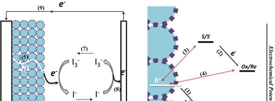
p-DSC is shown in Scheme 1.
Scheme 1. Simplified description of the working principle (left) and the electrochem-
ical potential diagram (right) for liquid p-type DSCs. The recombination processes
are symbolized by red lines. The white narrow bar in the electrochemical potential
diagram describes the potential of the edge of valence band (VB) of NiO. Ox/Re
means the redox couple composed by oxidized and reduced species. Detailed expla-
nation of the symbols used is given in the middle of Scheme 2.
Conventionally, in p-DSCs, dyes as light absorbers (ground state, S) are
promoted to their excited states (S*) through illumination. Holes injections
occur from the excited state of the dyes into the valence band (VB) of NiO,
resulting in formation of the reduced dyes (1). Then, the dyes are regenerat-
ed by electron transfer from the reduced dyes to the oxidized species of the
redox couple (2). The reduced redox species diffuse to the counter electrode
(6) and are regenerated by oxidation (8). The oxidized ions diffuse back to
the reduced dyes (7), to participate in the next cycle. At last, electrons col-
lected by the counter electrode (CE) transport to external circuit (9) to re-
combine with the holes which diffuse through the NiO matrix (5). In reality,
charge transfer does not exactly follow those desired processes mentioned
above. Recombination in the inner circuit is impossible to avoid, and is es-
pecially serious in p-DSCs[25,26]. Two common recombination pathways are
labelled in the electrochemical potential diagram of Scheme 1: (3) the re-
combination of the injected holes with the reduced dyes (non-geminate re-
combination); (4) the recombination of the injected holes and the reduced
species in the electrolyte (alien recombination).
15Scheme 2. Simplified description of the working principle (left) and the electrochem- ical potential diagram (right) for p-ssDSCs. The recombination processes are sym- bolized in red lines. The white narrow bar in the electrochemical potential diagram describes the potential of the edge of valence band (VB) of NiO. Detailed explana- tion of symbols is inserted. The liquid electrolyte can be replaced by solid-state electron transport mate- rials (ETM) to fabricate p-ssDSCs[27,28]. Through the design of solar cells, it is necessary to provide a diverse range of devices that are able to convert solar energy to electricity in ways tailored toward different requirements. P- ssDSC is one of those endeavors to that direction[29]. The solar energy con- version efficiency (up to 0.18 %[30]so far) is higher than that of 84 % of the liquid p-DSCs based on a reported review paper[31]in 2017 (referred to 174 cells), suggesting p-ssDSCs have the potential to be high-performance de- vice. The comparison of liquid and solid-state DSCs has been well summa- rized in review papers[32,33]. As for the working principle of p-ssDSCs, the reduced dyes are injected electrons to ETM (2), and then those electrons transport through the ETM to the counter electrode (6). The charge transfer processes and electrochemical potential diagram are similar as those of the liquid p-DSCs, as shown in Scheme 2. 1.3. Dye-sensitized NiO photocathode for solar fuels. The core concept of the solar fuel device is identical to any photoelectro- chemical system that involves the energy conversion processes: solar ener- gy—potential energy—chemical energy. In p-DSCs, electron transfer can be the reduced dyes transfer electrons to triiodide (I3-) and a new chemical, io- dide (I-) is produced. This can be considered as a photoelectronsynthetic process. In 1972, Honda and Fujishima designed a single crystal TiO2/electrolyte junction. In the system, holes generated by UV light occur onto the surface of TiO2, resulting in the 1st photoelectronsynthetic cell for water splitting[34]. Scheme (3) describes a photoelectronsynthetic cell focus- 16
ing on the dye-sensitized p-type photocathode. The electron acceptor can be
proton or CO2, and corresponding products H2[35] or carbon-based fuels[36]
can be expected to take place.

Scheme 3. Simplified scheme of the working principle in the photoelectrosythetic
cells based on dye-sensitized NiO photocathode for water splitting.

1.4. Scientific motivation.
By now, p-DSCs has been studied for two decades[23,37], but its solar energy
conversion efficiency is much lower than that of n-DSCs[38]. Why is that?
This should be the first question coming to the researchers’ mind when they
start working in this field. I intended to use a novel structure of p-ssDSCs to
explore new possibility to solve this problem; and devoted to give answers to
the questions: what is the mechanistic limitation of the new p-ssDSCs? What
is the possible limitation of mesoporous NiO photocathodes itself?

                                                                             17
2. Theory
In the chapter, theories related to charge separation, charge transport and
recombination will be briefly described in separate sections.
2.1. Planar semiconductor/electrolyte system.
Dye-sensitized crystalline planar semiconductor/electrolyte system was per-
formed in the initial development of DSCs[17,39]. In such system, the electro-
chemical potentials between the semiconductor and the electrolyte are not
equal. Charge exchange between the two systems will proceed once contact-
ing one another, and an equilibrium potential is formed through the whole
system. A depletion region is built up in the semiconductor with a band
structure bending upwards (assuming n-type semiconductor) in the high
ionic strength of electrolytes. Upon dye excitation, the electron is injected
into the conduction band (CB) of the semiconductor by tunneling (several
Ångströms)[40]. The electric field in the depletion region could promote the
injected electron to migrate away from the tunneling range, avoiding gemi-
nate recombination between the separated charges[41].
2.2. Mesoporous semiconductor/electrolyte system.
Grätzel cell is based on the dye-sensitized mesoporous semiconduc-
tor/electrolyte system[18]. The nanocrystals (10-20 nm in diameter) are inter-
penetrated but separate in space. The particle size should be smaller than the
depletion region in the planar semiconductor/electrolyte interface, provided
that the semiconductor is weakly doped (e.g. TiO2 based n-DSCs)[42]. The
band bending through the nanoparticle (i.e. the potential drop) can be rea-
sonable ignored considering the size of depletion width (in the planar semi-
conductor/electrolyte interface). In DSCs, each single nanoparticle in the
mesoporous film is surrounding by the electrolyte. The potential drop
through each nanoparticle will be even smaller[43].
After light excitation, the injected electrons from dyes into the nanocrys-
tal semiconductor are screened by the counter ions in the electrolyte, namely
the photoinduced electrons and screening counter ions can be treated as neu-
18tral pockets. Thus, the Coulomb repulsion among the injected electrons
could be ignored. This results in that no electric field is built in the nanocrys-
tal, like a surface charging sphere. Consequently, considerable amount of
charges can be injected into the nanocrystalline semiconductor without in-
ducing a significant electric field[44]. The screening process is mainly con-
trolled by the relaxation time of ions in the electrolyte. The relaxation time
in DSCs is commonly taken as infinite short and charge transport is domi-
nantly regarded as a diffusion process[44]. No potential drop is assumed in
most of the mesoporous semiconductor[45,46]. The potential drop is suggested
from the interface of the counter electrode (e.g. fluorine doped tin oxide
(FTO)) and the mesoporous semiconductor[46,47].
2.3. P-type semiconductor/dye/n-type semiconductor
system.
The energy diagram of the NiO-dye-TiO2 configuration is discussed here.
The p-type semiconductor NiO and n-type semiconductor TiO2 can construct
a p-n heterojunction (II)[48,49]. The formation of p-n junction is because the
charge exchange happens in the junction of NiO-TiO2, until an electric field
is formed to repel the majority in each semiconductor apart from the inter-
face. The role of the dye in the junction is essential to understand the energy
diagram in NiO-dye-TiO2 configuration. A thick and aggregated dye layer
on the planar semiconductor is suggested as an insulator/semiconductor
junction[21,41,50]. Longer time for charge exchange is required to reach a con-
stant equilibrium potential through NiO-dye-TiO2 configuration. Or such an
equilibrium condition can never be reached because of the inhibition of
charge exchange by the insulator of the dye layer. Combined with the dye
loading[51] and the surface area of the mesoporous NiO films[52], the NiO-
dye-TiO2 electrode (in this thesis) has been estimated with a sub-monolayer
dye adsorption if the dye is uniformly distributed. Charge exchange, through
the sub-monolayer dye, should be possible between NiO and TiO2. Ideally,
the dye stands up vertically on the inner surface of NiO. All dye are separate
one another, and no continuous band of the dye is built up. The junction in
NiO-dye-TiO2 can be treated as a conventional p-n junction in NiO-TiO2
with wide bandgap (Eg ≈ 3.5 eV for both NiO and TiO2)[53,54]. But the dye in
this interface is able to convert the visible light into the separated charges to
each semiconductor, as seen in Scheme 4.
19Scheme 4. The proposed p-n junction in a p-type semiconductor/dye/n-type semicon- ductor system. The depletion region in the p-n junction may be wider than the length of the dye[51], assuming most of the depletion region is localized inside TiO2 side (the hole concentration (p) in NiO is much higher than the electron concen- tration (n) in TiO2, p≫ n). Thus, the dye should be inside the electric field in the depletion region. The photo-generated hole and electron pairs are driven by such an electric field, and eventually separated in NiO (hole) and TiO2 (electron), respectively (Scheme 4). Such a configuration is able to reduce the recombination of the separated charge due to the energy barrier existing in the p-n junction. 2.4. Stark effect from photoinduced charge separation. In this section the Stark effect is briefly introduced since it is one of im- portant characteristics observed in NiO-dye-TiO2 configuration after pho- toinduced charge separation. Charge separation leads to the change of local electric field that is able to affect any charge transition or distribution. As most of dyes are in their electronic ground state, the Stark effect is seen as a shift of the ground state absorption spectrum of the dyes. Dye absorption is an electronic transition process, which can be considered as the interaction of transition dipole of the dye and the electric component of light (electro- magnetic wave), namely dipole-electric interaction[55]. Similarly, the transi- tion dipole of dye can be perturbed by an external electric field[56], resulting in absorption peak position (νmax) shifted to higher/lower energy which de- pends on the transition dipole is parallel or antiparallel to the external elec- tric field (only discuss the uniaxially oriented condition)[57]. The Equation (1)[56] is an expression of the final result with perturbation by the external electric field. The term on the left-hand side of the equation indicates the shifted absorption peak (in frequency). The two terms on right-hand side are the difference of potential energy wherein the first term relates to a perma- nent dipole moment, and the second term relates to an induced dipole mo- ment[57]. Those two terms also reflect the linear and quadratic dependence on electric field. 20
( )−         (0) = −Δ      − Δ                         (1)

In which,        ( ) and        (0) are the peak frequency in the pres-
ence/absence of electric field, respectively; E is the external electric field;
   and     are the difference dipole moment and polarizability between the
ground and excited states of the dye (Equation (1) is only in uniaxially ori-
ented condition).

By an expression of absorbance difference (ΔA), the linear term on the elec-
tric field can be described as Equation (2)[58] (the quadratic term is ignored
here since the ΔA commonly linearly depends on the electric field in dye-
sensitized semiconductor (the quadratic term is small)[59,60]).

                          Δ =−        ×     ×                             (2)

In which,     is the difference absorption; is the first derivative of ab-
sorption spectrum on wavelength; is the wavelength; c is the speed of light;
h is the Planck constant.

2.5. Charge transport and recombination.
For solar cells in the low injection condition, the flux of charge carriers in
specific area/time is described by the continuity equation[48] that is based on
the charge and mass conservation. The charge carriers in a given area are
dominantly influenced by the charge generation, recombination (treated as
the inverse flow of the current), and the current flow in or out this area under
the diffusion and drift induced by an electric field.

                         =    −   +     (       )+                         (3)

In which N is the concentration of charges; G is the charge generation rate;
R is the charge recombination rate; q is elementary charge; μ is charge mo-
bility; E is the electric field that imposes on charges; D is the charge diffu-
sion coefficient; x is the distance along the cross section of the solar cells.

As mentioned above, diffusion is the dominant charge transport mechanism
in conventional liquid DSCs[45,46]. Drift component (3rd term in the right-
hand side of the equation (3)) can be neglected. In the DSC system, the
charge generation rate and recombination rate can be further described as the
first term (following Beer-Lambert law) and the 2nd term (following the first-

                                                                             21
order reaction) on the right-hand side of the Equation (4), respectively. The
parameters of τ and D are fundamental to understand the charge recombina-
tion and diffusion after the photoinduced charge separation in DSCs.
( ) ( )
= − + (4)
Ф is the photon flux; α is the absorption coefficient; N(0) is the charge con-
centration in the boundary condition; τ is reciprocal of the recombination
rate (assume the 1st order reaction here).
2.6. Multi-trapping/detrapping model.
For an ideal planar crystalline semiconductor, the charge diffusion coeffi-
cient corresponds to the electron/hole diffusion coefficient in CB or VB,
given the electron diffusion coefficient in single crystalline TiO2 (ca. 0.4
cm2·s-1[61]), or hole in single crystalline NiO (ca. 0.05 cm-2·s-1)[62]. These val-
ues are orders of magnitude higher than the observed charge diffusion coef-
ficient in DSCs[63], indicating that the charge transport is influenced by the
mesoporous structure of the semiconductor films[64]. This could be ascribed
to the high density of trap states in the forbidden bandgap which involve in
charge transport, e.g. the multi-trapping/detrapping model shown in Scheme
(5). Based on this model, charge transport is described in three steps. (1) the
electron injection into the CB; (2) the electron trapped by the localized state;
(3) the electron detrapped back to CB by thermal activation. (4) the electron
transport in CB; (5) trapped again. Although the effective electron transport
(horizontal arrow in the Scheme 5) is completed inside CB, the multi trap-
ping-detrapping cycles reduce the electron transport rate, leading to a low
observed diffusion coefficient (Dd). Such phenomena can be described by
Equation (5) (TiO2 based)[65].
Scheme 5. The multi-trapping/detrapping model for electron transport. The dash
lines assigned as the localized trap states below CB.
22= 1+ (5)
Here, Dd is the observed charge diffusion coefficient; nL the density of elec-
trons in trap states; nc is the density of electrons in CB (free electrons); Dc is
the electron diffusion coefficient in CB.
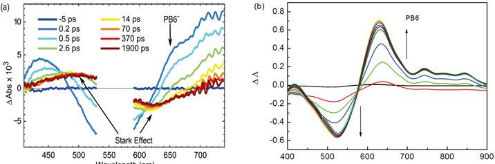
In contrast to TiO2, much less attention has been paid on the trap states in
mesoporous NiO films. The distribution of the trap states in NiO is very
distinguishing to that of trap states in TiO2 from both energetic and spatial
points of view. Generally, the trap states in TiO2 are treated as following an
exponential distribution below the edge of CB[65,66]. In NiO, from reported
results, the distribution of trap states is more similar to a Gaussian distribu-
tion[67,68]. The chemical nature of the trap states in NiO is still under debate.
Based on spectroelectrochemistry (SEC), those trap states were assigned as
Ni3+ and Ni4+ oxidized state[69,70]. Other researchers categorized part of them
as the oxygen-localized defect states[68,71], even Ni+ reported as the possible
trap states[72]. Nevertheless, the distribution, concentration and the chemical
nature of trap states affect the electronic properties of NiO, including the
charge diffusion in mesoporous NiO films. Until now, the mathematical
models of charge diffusion and recombination derived from TiO2 based n-
DSCs are directly applied into NiO based p-DSCs. However, these mathe-
matical models should be built individually for NiO based p-DSCs, consider-
ing the complex electronic properties (mentioned above), the high density of
trap states of mesoporous NiO films[43,67], and the significantly different die-
lectric constant of NiO from TiO2[43,73].
2.7. Hopping transport model.
Charge transport in a mesoporous semiconductor film can also be described
by a hole hopping model. In molecules, hopping transport is treated as
charges exchange reaction in an identical energy state[74,75]. In DSCs, hop-
ping transport model is applied since the trap states existed in the forbidden
band gap of the mesoporous semiconductors[76]. By hopping transport on a
semiconductor, the CB or VB is excluded for the charge transport, whereas
the charge transport is proposed through hopping among the localized states.
Here, the thermally activated hopping model of Miller-Abrahams equation
that has been used in DSCs is given as follow[76,77]. This model was original-
ly employed in amorphous semiconductor or polymers. Equation (6) shows
that the hopping rate is exponentially dependent on the difference of energy
and distance between localized sites. The charge transport rate requires inte-
gral of all the possible hopping steps. Since hopping indicates charge tunnel-
23ing from an occupied site to an empty one, it implies that charges around the
Fermi level have higher probability to perform such a leap.
−2 − , >
= (6)
−2 , ≤
v0 is the phonon vibration frequency (‘jump-attempt’ rate); r is the distance
between two localized states; α is localization radius which is from the result
of the overlap integral of the wavefunctions; Eem and Efi are the energy of
empty and the fill localized sates.
2.8. Ambipolar diffusion coefficient.
In the conventional liquid DSCs, the penetrated electrolyte inside the semi-
conductor matrix is the reason why the charge transport is only considered as
diffusion. Before Section 2.8, we assume that charge diffusion in semicon-
ductor is the only determining factor for the observed charge transport. Here,
the influence of the counter ions inside electrolyte is taken into account since
the counter ions compensate with the charges in the semiconductor. Many
reports showed that the concentration, conductivity and type of counter ions
of the electrolyte affected the observed charge diffusion coefficient[78-80].
Kopidakis et al. introduced the ambipolar diffusion coefficient[81] to explain
the influence of the electrolyte on the charges transport.
( )
= (7)
( / ) ( / )
Dabm is the ambipolar diffusion coefficient (analogous to Dd); n is the elec-
tron density; p is the hole density; Dn is the electron diffusion coefficient; Dp
is the hole diffusion coefficient.
With this model, the observed diffusion coefficient is dependent on the mi-
nority carrier. Note that n and p in the Equation (7) refer to the concentration
of those diffusible carriers (not fix charges). In conventional liquid DSCs,
the high concentration (relative to the photoinduced charge carriers in the
semiconductor matrix) of redox couples such as I-/I3- (50 mM) is commonly
applied. The redox electrolyte not only can eliminate the mass transport limi-
tation to the counter electrode, but also can make sure fast charge screening
to those injected charges inside the nanoparticles. Taking liquid p-DSCs as
an example, if the concentration of counter ions (n) in the electrolyte is much
higher than that of the injected holes (p), n ≫ p, this results in Dp can be
simply used to interpret the observed Dabm[82].
242.9. Charge screening in solid-state dye-sensitized solar
cells.
Here, I would like to discuss briefly whether the charge screening works in
solid-state DSCs (ss-DSCs). In comparison to liquid DSCs, the shortage of
free counter ions is the main difference for ss-DSCs. This could alter the
mechanism for charge transport since the injected charges are able to induce
an electric field without the effective charge screening[45,83]. Charge injection
could be limited as well by the Coulomb repulsion inside the nanoparticle.
Therefore, significant charge recombination is generally confirmed in ss-
DSCs[83-85]. Researchers also proved that the addition of free ions is able to
reduce the charge recombination, because of the improved charge
screening[86-88]. However, to my knowledge, no studies have been performed
on the influence of the existing electric field on the charge transport in ss-
DSCs. Diffusional transport is still widely applied in ss-DSCs[89,90].
Consider that the charges separate into each electron or hole conductor.
The concentration of the photoinduced charge should be identical in each
conductor. To screen electrons or the holes also requires careful investiga-
tion. By the inspiration from liquid DSCs, one strategy is to employ electron
conductor (TiO2) with high electron doping than the hole doping in NiO,
which causes that most of the space charge range localized in NiO (e.g. the
NiO-dye-TiO2 based p-ssDSCs). All the free holes in the NiO nanoparticle
are depleted. Surrounding the NiO nanoparticle, the higher doped conductor
(TiO2) with rich free electrons is able to fulfill the responsibility to screen
the injected hole in NiO (for n-ssDSCs, vice versa). Such a screening strate-
gy probably still could induce substantial charge recombination since both
separated carriers are in the solid phase, which is in analogous to the single
crystal solid-state solar cell[46].
253. Materials and methods The information of photosensitizer and important techniques/methods used are given in this chapter. Other methods can be found in the papers attached. 3.1. Sensitizer. In this thesis, a metal-free organic dye, PB6, with a donor-π-acceptor (D-π-A) configuration is used as the photosensitizer. A triphenylamine (TPA) unit and a perylene monoimide (PMI) group are chosen as the electron donor (D) and acceptor (A) moiety, respectively, linked by a thiophene group (π linker). The structure (left) and the absorption spectrum (right) of PB6 dye can be found in Scheme 6. Scheme 6. Structure of PB6 dye with a D-π-A configuration and UV-vis absorption spectrum in dichloromethane (DCM). PB6 dye was newly synthesized with highly chemical and thermal stability similar as reported perylene-based chromophores[91]. The PB6 dye also shows reversible and spectrally distinguishable reduced state and oxidized state. The electrochemical characterization of PB6 is summarized in Table 1. 26
Table 1. Electrochemical characteristics of PB6.

Note: E0-0 is the energy difference between the electronic ground state and the lowest excited
singlet state of the PB6 dye, which is similar as the energy difference between the highest
occupied molecular orbital (HOMO) and the lowest unoccupied molecular orbital (LUMO).
E1/2(s+/s) and E1/2(s/s-) are the formal reduction potentials in the ground state of PB6.
E1/2(s+/s*) and E1/2(s*/s-) are the formal reduction potentials in the excited state of PB6.

3.2. Atomic layer deposition (ALD).
Atomic layer deposition (ALD) technique is one of the technologies for the
preparation of ultrathin films. ALD is able to satisfy the demand of an atom-
ic layer control and conformal coating, using sequential and self-limiting
surface chemical reaction through gas phase. The most outstanding ad-
vantage of ALD is that it can practically achieve desired thickness at the
Ångström level. Most of the ALD are binary reaction sequences including
the ALD used in this thesis[92]. Here, a simplified schematic description is
given to understand the working principle of this technique (Scheme 7). In
this thesis, three metal oxides (TiO2, ZnO and Al2O3) were prepared with
ALD technique. The precursors for ALD TiO2 are titanium tetrachloride
(TiCl4) and H2O, diethylzinc (DEZn) and H2O for ALD ZnO, and trimethyl-
aluminum (TMA) and H2O for ALD of Al2O3.

Scheme 7. Simplified one ALD cycle. #1: the target film; #2: pulsing precursor A
with 1st chemically adsorbed layer. #3: removing the non-chemical adsorbed layer
by N2 purge; #4: pulsing precursor B to perform the chemical reaction between A
and B. #5: N2 purge to remove the non-chemical adsorbed B. The binary chemical
reaction is inserted.

                                                                                          27
3.3. Current-voltage (I-V) characterization.
Current-voltage (I-V) measurement should be the most important characteri-
zation of solar cells which directly provides the well-known characteristic
parameter: solar energy conversion efficiency (η). The measurement is per-
formed by scanning the bias potential between the working electrode and
counter electrode of solar cells. The measurement is commonly employed in
the dark or light mode. A forward or a reverse bias potential can be also im-
posed at each mode.
In an ideal case, the I-V measurement is equivalent to impose a scanning
potential on a diode under the dark mode[48,93]. It is possible to extract the
properties of a given solar cell, like the ideality factor, shunt resistance and
series resistance. Under illumination, the whole I-V curve is supposed to be
shifted downward (Figure 1). The photocurrent flows oppositely compared
to the dark current under forward-biased scanning. In I-V curve, the potential
under the net zero current is called open-circuit voltage (Voc) in which the
photocurrent is equal to the dark saturated current. Beyond the Voc the fea-
ture of the diode of a solar cell will be quickly lost, and then the I-V curve
will be described by Ohm’s law. Under the reverse bias, the photocurrent
density (Jp) is the difference of the current density under illumination (Jp + J0)
and dark (saturated current J0). The short-circuit current density is Jsc= Jp +
J0 which is the current density without any external potential applied. Jsc can
be simply treated as Jp if J0 is negligible (Equation (8)).
3
Dark
2 Light
1
'
V oc
-2
0
J/mA⋅cm
Voc
-1
-2 '
J sc
-3
Jsc
-4
-0.05 0.00 0.05 0.10 0.15
Voltage/V
Figure 1. Illustration of J-V plot. The J-V curve was measured from p-DSCs with
NiO-PB6 as the photocathode and 50 mM I-/I3- in acetonitrile as redox couple. (J
means the current density (mA·cm-2))
28= − −1 (8)
Here, J is the net current density; Jp is the photocurrent density; J0 is the
saturated dark current density; q is the elementary charge; V is the applied
bias potential; n is the ideality factor; kB is the Boltzmann constant; T is the
Kelvin temperature.
The performance of solar cells is also widely evaluated by a so-called fill
factor (FF) (defined by Equation (9)) which generally describes “bad” or
“good” of the solar cells, like the solar energy conversion efficiency. Any
energy loss is dumped into such a mathematical parameter. With the FF, the
solar energy conversion efficiency can be calculated from Equation (10).
′× ′
= (9)
×
′ × ×
= = (10)
In which, ′ is the voltage in the maximum power output; ′ is the current
density in maximum power output; p’ is the maximum power output. Pin is the
power of the incident photons.
3.4. Incident photon-to-current conversion efficiency
(IPCE).
Generally, I-V measurement is performed under simulated sun light, indicat-
ing that photocurrent and photovoltage result from the broad solar spectrum.
The individual contribution of the photocurrent from a single wavelength
cannot be extracted in such an I-V measurement. Therefore, IPCE is used to
tell the contribution of the photocurrent at each wavelength. IPCE in litera-
tures are also referred to the external quantum efficiency or the action spec-
trum. IPCE essentially provides the ratio of the achieved electrons/the inci-
dent photons. What we can directly measure are the output photocurrent and
the input photo flux, as shown in Equation (11). Isc is the short-circuit current.
( ) ( )
φ (λ) = = × × 100 (11)
( ) ( ) ( )
The Equation (11) only considers the result of the input (photons) and the
output (electrons). IPCE can be theoretically calculated from a kinetic path-
way to trace how a photon converts into an electron step by step, described
in Scheme 1. To extract a photo-generated electron several processes are
29involved which is from the photon absorption, charge injection and dye re-
generation, to the charge collection, expressed by Equation (12)[94,95].
= × × × (12)
LHE is the light-harvesting efficiency; Φinj is the charge injection efficiency;
Φreg is the dye regeneration efficiency and Φcc is the charge collection effi-
ciency.
To integrate the photocurrents from each wavelength, the photocurrent from
whole solar spectrum also can be obtained, as shown in Equation (13).
Commonly, the IPCE measurement is performed under short-circuit condi-
tion, so the integrated current density from IPCE should match with the Jsc
measured from the J-V characterization.
= ( ) ( ) (13)
Here, λ1 and λ2 are the integration wavelengths. E(λ) is the single photon
energy at wavelength λ.
However, the energy conversion efficiency cannot surpass the Shockley-
Queisser limit[24] in the DSCs with a single dye. The reason is due to that
part of photons below Eh-l (Eh-l, the energy difference between the HOMO
and LUMO of the dye) cannot be absorbed, and those photons beyond Eh-l
have to dissipate additional energy into heat from the hot electrons. There-
fore, the tandem DSCs with multi-junctions (dyes) are expected to surpass
the Shockley-Queisser limit in order to significantly improve the IPCE value
from each wavelength.
3.5. Transient photovoltage measurement.
Charge recombination is an important kinetic process causing the energy
loss in DSCs, commonly described by a parameter called charge lifetime (τ)
(Equation 4). In practice, it is impossible to directly measure the charge con-
centration[96,97]inside a DSC. The decay of Voc is employed to extract the
charge lifetime, because Voc and charge concentration (n) can be connected
by Equation (14)[98]. In addition, no net current flows under open-circuit
condition, suggesting the charge loss results from recombination. The Fermi
level under dark condition is constant through the whole solar cell because
of the thermal equilibrium. Under illumination, a photovoltage is built up
after charge injection into the semiconductor, corresponding to a new Quasi-
Fermi level (photo-generated electrons alter the thermal equilibrium). The
30charge recombination in different Quasi-thermal equilibrium conditions can
be derived R=R0exp(ΔEF/nkBT)[99] (R is recombination rate, R0 is recombina-
tion rate in dark and ΔEF is the Quasi-Fermi level splitting; n is the ideality
factor; kB is the Boltzmann constant; T is the kelvin temperature).
= = (14)
Here, nc is the electron concentration in the CB under light; n0 is the elec-
tron concentration in the CB under dark; EFn is the Quasi-Fermi level under
light; EF0 is the Fermi level under dark.
Transient photovoltage measurement is performed on a given solar cell illu-
minated by a specific light intensity (corresponding to a specific state of this
solar cell). Then, a small light intensity is imposed above the specific light
intensity to perturb the original state of the solar cell. The changing Voc is
traced, which is chosen as a parameter to describe the changing states. Here,
the ‘small’ means charge recombination rate constant does not change under
the external light perturbation[100] (assume the charge recombination is a
pseudo-first order reaction). Then, the charge lifetime on a fixed light inten-
sity can be extracted from the Voc decay by an exponential fitting.
As is well known, there is a high density of surface states localize on the
mesoporous semiconductors. Those trap states are able to alter the observed
charge recombination process, which has been proven in the n-DSCs. A
physical model[100] suggested by Bisquert provided a mathematical explana-
tion on the influence of trap states on the charge lifetime of DSCs. The mul-
ti-trapping events increase the observed charge lifetime because those
trapped electrons require time to detrap into the CB in TiO2 before the effec-
tive transport occurs. The charge recombination is assumed to occur only in
the CB (free electron), as seen Equation (15). The physical meaning of a
measured charge lifetime could be more complex because of multiple kinetic
processes involved, such as the charge recombination with trap states in bulk,
or surface states, and the recombination between the charge in surface states
and the electrolyte.
= 1+ (15)
Here, τ is the observed electron lifetime; τc is the electron lifetime in the CB
(without the influence of trap states); nL is the electron density in trapped
states; nc is the electron density in conduction band;
313.6. Transient photocurrent measurement.
Transient photocurrent is also a small perturbation technique of light intensi-
ty, similar as the transient photovoltage mentioned above. The purpose of
such a measurement is to study the charge transport behavior in a connected
circuit after photoinduced charge separation. The standard measurement is
performed under a short-circuit condition and the in-time Jsc decay is moni-
tored. The corresponding response time (τrep) is then extracted from the Jsc
decay. Since charge recombination happens during the charge transport, the
observed response time should be described as Equation (16). Generally,
charge recombination is much slower than the charge transport under short-
circuit condition. The response time basically is equivalent to the charge
transport time.
= + (16)
Here, τrep is observed response time; τtr is the charge transport time, and τre
is the charge lifetime under short circuit condition.
With charge transport time, charge diffusion coefficient can be calculated by
Equation (17)[101]. The coefficient of β is determined by the particular
transport path in a mesoporous semiconductor, which could be affected by
the trap states.
= (17)
Here, Dd observed charge diffusion coefficient; d is the thickness of the mes-
oporous film. τtr is the charge transport time; β is a constant coefficient.
In addition, the transient photocurrent can be measured under different light
intensity with on/off modes. In this situation, the trap states should be empty
in the dark. The trap filling process can be traced after light perturbation by
following the transient photocurrent. The shape of the transient photocurrent
curve (vs. time) can be even used to identify charge transport mechanism. In
DSCs, the transient photocurrent observed gradually increases until reaching
an plateau, which can be affected by light intensity[102] and the frequency of
perturbation[103]. The charge trapping/detrapping in the localized sates has
been treated as the main reason for such a behavior during the measurement
of transient photocurrent. The transient photocurrent measurement is also
performed in a semiconductor via bandgap excitation. Photocurrent shows
similar behavior (gradually increases until reaching an equilibrium state) as
these measurements without a pre-imposed bias light, which seems to be
32affected by the same trap filling process. The photocurrent can steeply in- crease when the bias light is applied[104]. 3.7. Transient absorption spectroscopy (TAS). UV-vis absorption spectroscopy is based on Beer-Lambert law = − ( / ) by directly detecting transmitted light (assuming A is the steady state absorption; I is the transmitted light intensity; I0 is the incident light intensity). TAS is used to trace the kinetics of the target species/process after perturbation of the steady state. Commonly, a pump laser is used to perturb the sample, and then a polychromatic laser is to probe absorption of the tran- sient species/process in different time delays. The probe process is identical as the measurement of steady state absorption, = − ( / ) (A is the absorption of the transient species/process; is the transmitted light intensi- ty after pump). In TAS, the difference absorption spectrum is used to distin- guish the absorption of different species/process, = − = ( / ). Thus, ΔA is zero if I= Ip; ΔA is a positive signal if I>Ip, vice versa. Three absorption features are generally observed in TAS, (1) ground state bleach (IIp); (3) stimulated emission (I
You can also read