Graphenic carbon as etching mask: patterning with laser lithography and KOH etching - mediaTUM
←
→
Page content transcription
If your browser does not render page correctly, please read the page content below

Journal of Physics: Conference Series

PAPER • OPEN ACCESS

Graphenic carbon as etching mask: patterning with laser lithography and
KOH etching
To cite this article: A Furio et al 2019 J. Phys.: Conf. Ser. 1226 012011

View the article online for updates and enhancements.

                              This content was downloaded from IP address 129.187.254.46 on 30/04/2020 at 08:16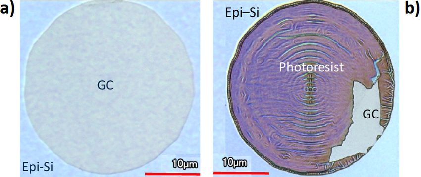
9th Young Researcher Meeting                                                                                    IOP Publishing
IOP Conf. Series: Journal of Physics: Conf. Series 1226 (2019) 012011                     doi:10.1088/1742-6596/1226/1/012011

Graphenic carbon as etching mask: patterning with
laser lithography and KOH etching
                      A Furio1,2 , M Stelzer1 , M Jung1 , H C Neitzert2 , F Kreupl1
                      1
                          Technical University of Munich (TUM), Arcistr. 21, Munich, Germany
                      2
                          University of Salerno, Via Giovanni Paolo II 132, Fisciano, Italy
                      E-mail: furioalfonso@gmail.com

                      Abstract. The wet anisotropic etching process is generally used in the field of micromachining
                      (MEMS), particularly for commercial products such as accelerometers. Hard masks like oxide
                      or nitride play a key role in the transfer of patterns to the substrate during the lithography
                      process. This work reports on the use of polycrystalline graphenic carbon as an etch mask for
                      wet chemical processing and outlines a simple method to create patterned structures on (100)
                      silicon wafers. Graphenic carbon (GC) was deposited on the silicon substrate by chemical vapor
                      deposition (CVD) using C2 H4 as precursor. The desired pattern was written in the spin-coated
                      negative photoresist using UV laser lithography. Different geometrical shapes were printed on
                      the substrate with dimensions ranging from 10 to 50 micrometers. In the next stage, the O2
                      plasma etched away the carbon from the area not covered by the photoresist, acting as an
                      additional mask for this and the subsequent processing steps. Finally, the sample was immersed
                      in the KOH bath saturated with isopropanol and the etching rate was evaluated for each crystal
                      plane. Compared to the use of a sacrificial oxide mask, this technique is simpler and produces
                      more reliable results.

1. Introduction
Anisotropic wet etching is one of the most used techniques for fabricating 3D structures as
MEMS on silicon substrates. Particularly, bulk etching is widely used to remove silicon from
the substrates in order to produce sensors or actuators. Typical micromechanical devices,
manufactured on (100) silicon wafer, are cantilevers or membranes that usually need supporting
structures based on oxides or nitrides [1]. These insulating hard masks also play an important
role during the lithography step for transferring patterns to the substrates. The etching process
is usually carried out in an aqueous solution of KOH, but as reported by Barycka et al. [2], the
KOH solution saturated with isopropyl alcohol is the most frequently used to obtain a high
etch rate ratio and smooth surface on (100) silicon. The choice of the etching solution depends
on different factors such as etch rate and anisotropy. The etch rate differs between the crystal
planes and the concentration of the used solution [3, 4]. The aim of this work is to create
3D structures on (100) silicon wafer using photolithography and wet anisotropic etching in a
commonly used solution of KOH and isopropanol. In this context, the use of graphenic carbon
(GC) [5, 6] as an etching mask instead of sacrificial oxide is a new feature. As reported in [7, 8],
it is possible to form GC membranes on one side of a wafer exploiting the undercut created by
the KOH (saturated with isopropanol) on a silicon substrate. GC is a good candidate for the
future process due to the fact that it is inert to most common solvents such as acetone and NMP

              Content from this work may be used under the terms of the Creative Commons Attribution 3.0 licence. Any further distribution
              of this work must maintain attribution to the author(s) and the title of the work, journal citation and DOI.
Published under licence by IOP Publishing Ltd                          1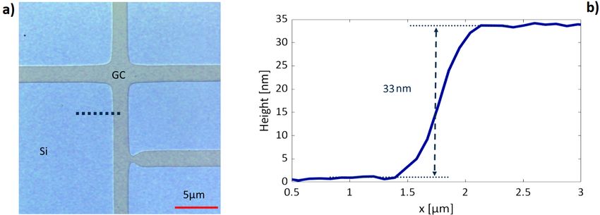
9th Young Researcher Meeting                                                                  IOP Publishing
IOP Conf. Series: Journal of Physics: Conf. Series 1226 (2019) 012011   doi:10.1088/1742-6596/1226/1/012011

and, with a thickness of a few nanometers, it is resistant to HF and KOH. Another advantage is
that it is extremely easy to remove with a O2 or H2 plasma and that it is compatible with the
CMOS standard process through chemical vapor deposition (CVD). Moreover, the thickness of
the GC is easily tunable by controlling the parameter of the deposition. The high-temperature
stability, the low contact resistance to silicon and the endurance to high current densities make
this material the ideal candidate for metal-silicon contacts [9]. In the process flow of this work,
this means saving process steps using a conductive mask.

2. Sample preparation
The substrate used for this work is a n-type silicon wafer, doped with arsenic (ρ = 0.01 Ωcm)
covered by an epitaxial layer with a thickness of 8 µm, doped with phosphorus (ρ = 0.75 Ωcm).
The crystallographic orientation of the surface is in the (100) plane. The wafer used for the
samples was cut in pieces of 1 cm x 1 cm with a thickness of 625 ± 25 µm.

2.1. Substrate cleaning
During the fabrication process, the contamination of particles on the surface of the wafer needs
to be avoided in order to have a clean substrate for the further steps. A smooth and clean
surface is necessary to deposit effectively a uniform graphenic carbon film. First, the sample
was placed in acetone at 60 ◦C and sonicated for 10 min, in order to remove the protective resist
layer. Next, the sample was put into isopropyl alcohol and sonicated with the same previously
reported conditions to remove the acetone residuals not soluble in water. Afterward, the sample
was prepared with a full RCA clean [10]. The standard cleaning SC-1 was done at 75 ◦C for
10 min to eliminate the organic residuals. After that, the standard cleaning SC-2 was performed
at 75 ◦C for 10 min to remove ionic contaminations due to metallic particles on the surface.

2.2. Graphenic carbon deposition
Before the carbon deposition, it is necessary to dip the sample in 5% hydrofluoric acid (HF) for
150 sec to remove the native oxide. The deposition was performed with a low-pressure chemical
vapor deposition (LPCVD) process at 1000 ◦C. The used precursor was C2 H4 with a gas flow
of 20 sccm and the pressure in the chamber was 20 mbar. This deposition was carried out for
7 min to obtain the desired layer of GC [6, 9].

2.3. Laser lithography
The lithography process is used to transfer the patterns to the substrate using a spin-coated
negative photoresist and a UV laser. Firstly, the sample was heated on a hotplate up to 200 ◦C
for 30 min to remove the adsorbed humidity and afterward, the resist ma-N 1420 was spin-coated
on the cooled substrate at 3300 rpm for 30 sec. Next, the sample was heated for 90 sec at 100 ◦C
to remove the solvents from the resist. In order to generate the desired structure, the surface of
the sample was exposed to the focused laser beam of the KLOÉ Dilase 250 laser writer with a
laser wavelength of 375 nm and a power density of 351 kW cm−2 . Fig. 1 shows the process steps
and the result after the laser lithography. The key parameters to control the design are the
modulation of the laser intensity, the velocity of the stage, the focal plane, the exposure time
and the possibility to apply three different optical filters. The minimum spot size of the laser
is 1 µm but changing the focal plane a spot size around 100 µm has been obtained. The writing
process requires only few minutes to produce more than hundreds of reproducible shapes using
velocity and repositioning velocity of 2 mm s−1 . Finally, the sample was dipped in ma-D 533/s,
which is a developer that removes the unexposed resist in around 1 minute. This developing
time is particularly critical and can directly affect the geometric property and the resolution of
the pattern.

                                                       2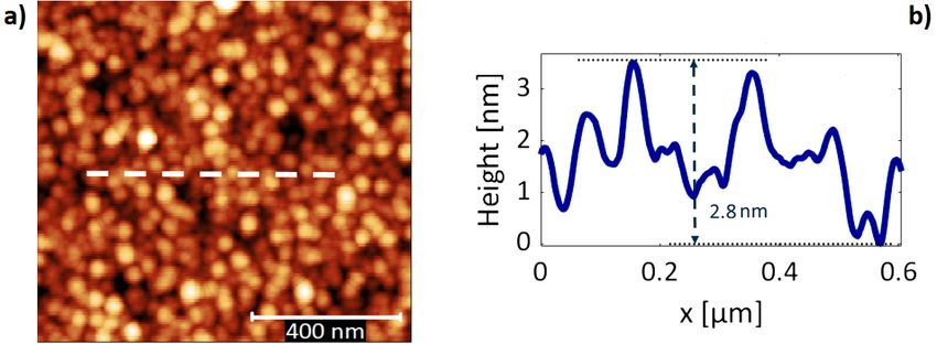
9th Young Researcher Meeting                                                                  IOP Publishing
IOP Conf. Series: Journal of Physics: Conf. Series 1226 (2019) 012011   doi:10.1088/1742-6596/1226/1/012011

2.4. Dry etching
The RF plasma process was used to remove the carbon from the area that is not covered by the
resist. The pressure in the chamber was 2 mbar for a H2 plasma and around 0.5 mbar for a O2
plasma respectively. The effects of both plasmas were compared and evaluated under different
conditions. The etching time was always set at 3-times 10 sec with 30 sec of cooling time. In
the Fig. 2, the process steps and the result are shown. After the plasma etching, the resist was
removed as reported in Sec. 2.1.

                                                            Figure 2.       After the development of the
Figure 1.     Certain areas of the surface are              resist, the pattern is created in the carbon by
exposed to the focused laser beam to generate               etching the carbon away. The process steps are
the desired pattern (a). An example of the                  illustrated in (a). (b) shows an optical true
exposed and developed circular resist pattern is            color image of a structure after removal of the
shown in (b).                                               resist.

2.5. Wet etching
Before being dipped into the KOH bath, the sample was immersed into HF for 30 sec to remove
the native oxide that could delay the silicon etching. A 5 M solution of KOH saturated with
isopropanol was heated up at 80 ◦C in a constant-temperature water bath and the sample was
immersed for 9 min. After that, decontamination with the SC-2 cleaning was carried out for
30 min. The final result of this step and the relative schematic is reported in Fig. 3.

                      Figure 3. After the pattern of the carbon layer by plasma
                      etching, the native oxide was removed by a HF bath and the
                      silicon was etched away using KOH saturated with isopropanol.
                      a) Shows a schematic of the wet etching result. b) (top view)
                      3D laser image of the circular structure after the wet etching
                      process.

3. Results
In order to determine the presence of the GC on the substrate, Raman spectroscopy is used
with a laser excitation at 532 nm. The D and G bands are the most relevant ones for the GC

                                                       3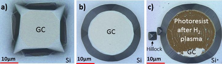
9th Young Researcher Meeting IOP Publishing
IOP Conf. Series: Journal of Physics: Conf. Series 1226 (2019) 012011 doi:10.1088/1742-6596/1226/1/012011
spectrum and are shown in Fig. 4.
Figure 4. Raman spectra of GC after a deposition of 33 nm on silicon
substrate (blue) and silicon without GC (red).
The Raman shift associated with the D and G peaks are at 1350 cm−1 and 1584 cm−1 . As
reported by [11], the high content of covalent sp2 -bonds is highlighted by the height of the G
peak compared to the D peak. After the plasma dry etching, the GC is removed and the two
silicon peaks at 520 cm−1 and 960 cm−1 are clearly visible. After the GC deposition, as described
in Sec. 2.2, the surface roughness of the film was measured with an atomic forced microscopy
(AFM) set in tapping mode in order to not damage the surface. The root mean square height
(Sq) is 1.3±0.1 nm and the dashed white line in the Fig. 5 (a) shows the section where the profile
of the film was evaluated. The thickness of the GC was measured with a 3D laser microscope
(Keyence VK series) on a sample patterned with lines and crosses through the laser lithography
and after the removal of the carbon from the area not covered by the resist by dry etching. In
this way, a step to evaluate the height of the GC deposition was obtained. The dashed black
line in the Fig. 6 (a) shows where the analysis was taken and the Fig. 6 (b) shows the step with
the height of 33 ± 1 nm.
Figure 6. a) 3D laser microscope image of
Figure 5. a) AFM image of a silicon sample after a GC cross. b) Cross profile to determine the
a deposition of GC. b) AFM profile of GC. thickness of the GC deposition.
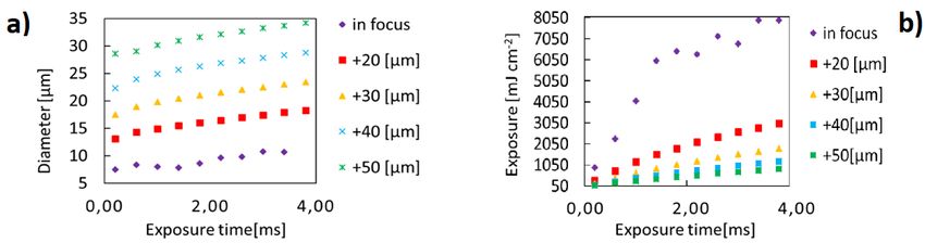
Concerning the laser lithography, the resist used has a thickness of 2 µm using the spin coating
parameters reported in Sec. 2.3. It was investigated how to obtain different diameters during
the writing process by setting the focal plane, the exposure time and the modulation. In the
plot (a) of the Fig. 7 the diameter function of the exposure time for different focal planes, at fixed
modulation (80 %) and without a filter it is shown. In the plot (b) of Fig. 7 the exposure dose
function of the exposure time at a different focal plane and at fixed modulation it is illustrated.
The value of the exposure dose D was evaluated according to the following equation:
P·m
D= ·t (1)
(π r2 )
4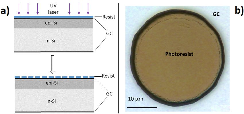
9th Young Researcher Meeting                                                                   IOP Publishing
IOP Conf. Series: Journal of Physics: Conf. Series 1226 (2019) 012011    doi:10.1088/1742-6596/1226/1/012011

Figure 7. a) Experimental plot of the dot diameters function of the exposure time at fixed modulation
and focal plane. b) Plot of the exposure dose transferred to the resist, function of the exposure time, at
fixed focal plane and modulation. The relative error is ± 1.1%

where t is the exposure time, m is the laser power modulation (in %), r is the radius of the
printed dot and P is derived from the maximum power density (351 kW cm−2 ) given by the
manufacturer and divided by the area of the laser spot with a diameter of 1 µm (resolution
of the machine). This last calculation is only theoretical and was not yet been validated by
measurements due to the complicated setup. However, the exposure dose required, as stated in
the resist datasheet, is around 550 mJ cm−2 and it was always surpassed with the combination
of the chosen parameter during the laser writing. Fig. 8, shows the effects of both plasmas on
the resist mask. Mainly, due to the higher energy at a lower wavelength for the H2 plasma
(Lyman series), as depicted in Fig. 8 (b), the resist was hard baked and it was no longer possible
to remove even after repeated cleaning in acetone and NMP. This is also confirmed by the
absorbance coefficient of the resist, which shows a peak at a wavelength under 250 nm. In some
cases, the resist hardbake occurred only at the boundary of the resist, due to the fact that this
effect is strictly dependent on the previous process conditions modifying parameters such as
the resist thickness. Therefore, the O2 plasma was chosen for reliable and repeatable results
as shown in Fig. 8 (a). The last evaluation was regarding the wet etching process. Using the
Keyence 3D laser scanner as an optical profilometer, the side a and the angle α reported in the
schematic in the Fig. 9 (a) were measured for each plane as shown in Fig. 9 (b).

Figure 8.       Comparison between two different           Figure 9.      a) Schematic of the crystal plane
plasmas during the dry etching process. a) effect of       section. b) 3D laser scanner image of a circle (top
O2 plasma on a circular resist pattern. Next, the          view) with a diameter of 31 µm. The wet etching
resist over the GC layer was successfully removed          step was performed for 9 min and the absolute
by solvents. b) hardbake effect on the resist after        height obtained is 8.9 µm. The investigated planes
H2 plasma on a circular resist pattern.                    are highlighted, the other planes are symmetric [2].

   Using the right-angled triangle definition:
                                               c = a · cos(α)                                              (2)
and divide by the etching time the etch-rate for each crystal plane is estimated as reported in
the Tab. 1.

                                                       5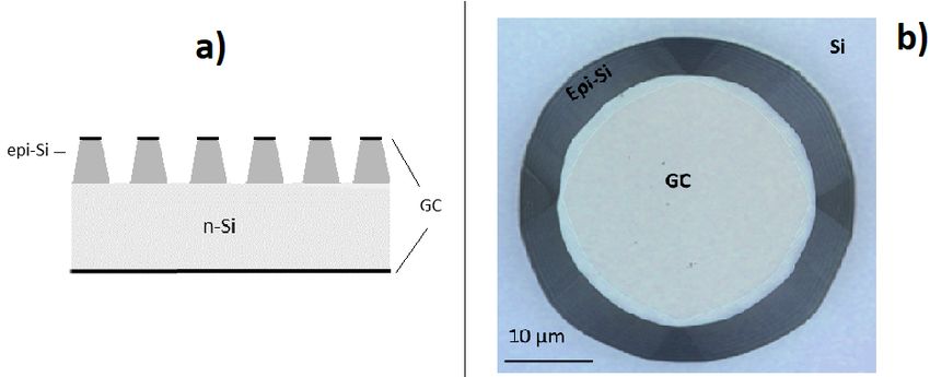
9th Young Researcher Meeting                                                                     IOP Publishing
IOP Conf. Series: Journal of Physics: Conf. Series 1226 (2019) 012011      doi:10.1088/1742-6596/1226/1/012011

Table 1. The etching rate (second row), expressed in µm min−1 , evaluated for each crystal
plane (first row).
                                      (100)    (111)       (313)   (101)
                                       0.82      0.1       0.13    0.15

   Fig. 10 shows a comparison between the use of KOH without isopropanol (a) and with
isopropanol (b). In Fig. 10 (c) two problems are highlighted: the first concerning the effect
of the H2 plasma on the resist, as discussed before, and the second regarding the missing dip in
HF before the KOH bath that produces hillocks on the substrate.

Figure 10. a) Effect of wet etching with (5M) KOH not saturated with isopropanol. b) Effect of wet
etching: first HF(5 % ) dip for 20 sec and after (5M) KOH saturated with isopropanol. c) Effects of H2
plasma on the resist and (5M) KOH saturated with isopropanol without a prior dip in HF(5 % ) and a
resulting hillocks formation on the surface.

4. Conclusions
In conclusion, an easy method to pattern different shapes on (100) silicon substrates is shown.
The polycrystalline GC as an etch mask for wet chemical processing offers different advantages
such as excellent adhesion to silicon due to the formation of covalent bonds during the deposition,
material thinness, resistance to common solvents, aggressive acids (HF) and bases (KOH), easy
and quick removal by O2 plasma. Furthermore, it is an excellent conductive material that could
be directly used as a stable contact.

5. References
[1] French P J et al. 1997 Sensors and Actuators A: Physical 62
[2] Barycka I et al. 1995 Sensors and Actuators A: Physical 48
[3] Zubel I et al. 2004 Sensors and Actuators A: Physical 115
[4] Zubel I et al. 2002 Sensors and Actuators A: Physical 101
[5] Bianco A et al. 2013 Carbon 65
[6] Kreupl F 2011 MRS Proceedings 1303
[7] Huebner S et al. 2015 IEEE Transactions on Nuclear Science 62
[8] Reinhard D K et al. 2004 J. Vac. Sci. Technol. B: Microelectr. Nanom. Struct.22
[9] Stelzer M et al. 2017 IEEE Journal of the Electron Devices Society 5
[10] Kern W 1990 Journal of the Electrochemical Society 137
[11] Pimenta M A et al. 2007 Phys. Chem. Chem. Phys. 9

                                                       6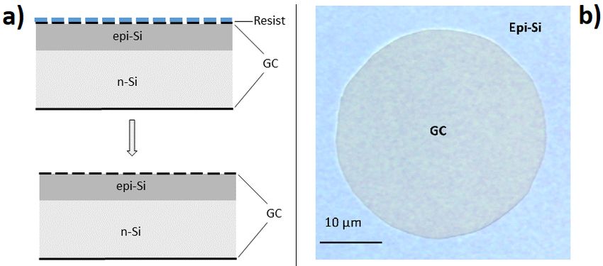
You can also read