MICROFABRICATION Alessandro MAPELLI - DT Group Meeting, 22 June 2017 - CERN Indico
←
→
Page content transcription
If your browser does not render page correctly, please read the page content below
Alessandro MAPELLI DT Group Meeting, 22 June 2017

MICROFABRICATION
 Anastasia Jacopo Timothée Georgi Ranit Luca Clémentine Ludovic
BERDNIKOVA BRONUZZI FREI GORINE MONGA MÜLLER LIPP SEREX
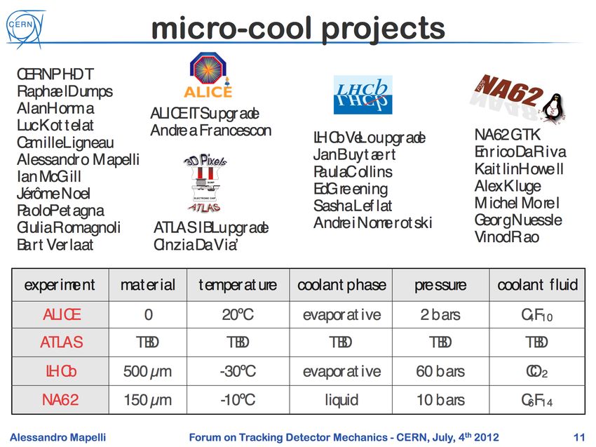
MICROFABRICATION OF ON-DETECTOR COOLING SYSTEMS
Fabrication of structures with features below the mm.
Same techniques as used for microelectronics and silicon detectors.
 Novel high performance compact systems based on microfluidics.
 ical
 d on Plastic Opt
 til la tio n Pa rti cl e Detectors Base
 Scin

 (2011)
 THÈSE N 5033
 O

 2011
 2 SEPTEMBRE
 PRÉSENTÉE LE
 HN IQU ES DE L'INGÉNIEUR
 IENCES ET TEC

 g
 À LA FACULTÉ SC

 i n
 ES 4

 l
 TÈM

 o
 RO SYS

 o
 DE MIC

 c
 LABORATOIRE CTRONIQUE

 el
 ES ET MICROÉLE

 an n
 MICROSYSTÈM

 Silicon microch
 CTO RA L EN
 PROGRAMME DO

 ANNE
 RALE DE LAUS
 CHNIQUE FÉDÉ
 ÉCOLE POLYTE
 SCIENCES
 DE DOCTEUR ÈS
 ON DU GRADE
 POUR L'OBTENTI

 w ell, A. Klug e, A. Map elli, M. Morel, J. Noel,
 guin, R. Dumps, K. Ho
 J. Buytaert, A. Catinaccio, J. Da
 PAR

 L), G. Ro m ag no li, J. Thome (EPFL)
 LI ssle, P. Petagna, Ph. Re
 ELue
 MAPN
 na ud (E PF
 AlessandroG.

 Nuclear Physics B (Proc. Suppl.) 215 (2011) 349–352
 www.elsevier.com/locate/npbps
 position du jury :
 acceptée sur pro

 Prof. M. A. Ionesc
 Prof. Ph. Renaud
 u, président du jury
 , Dr P. L. G. Grafstr
 öm, directeurs de
 , rapporteur
 thèse Low material budget microfabricated cooling devices for particle
 Prof. A. Bay
 Dr B. Gorini, rap
 Dr M. Haguenaue
 por teu r
 r, rapporteur detectors and front-end electronics
 A. Mapelliab ∗ , A. Catinaccioa , J. Daguina , H. van Lintelb , G.Nuesslec , P. Petagnaa , P. Renaudb ,
 a
 Physics Department, CERN, Geneva, Switzerland
 b
 Laboratoire de Microsystèmes, Ecole Polytechnique Fédérale de Lausanne, Switzerland
 Suisse
 2011 c
 CP3, Université catholique de Louvain, Louvain-la-Neuve, Belgique
 Novel cooling systems with very low material budget are being fabricated and studied. They consist of silicon
 wafers in which microchannels are etched and closed by bonding another wafer. This cooling option is being
 considered for future HEP detectors of the sLHC and linear colliders. It is currently under investigation as an
 DT Group Meeting,
 option22
 forJune 2017 of the NA62 Gigatracker silicon pixel detector and its front-end
 the cooling Alessandro
 electronicsMapelli | 2
 where the
 microfabricated cooling plate would stand directly in the beam. In this particular case, microchannel cooling
WHY MICROFLUIDIC ON-DETECTOR COOLING SYSTEMS ?
d Integrated Micro
 Micro-channel
 channel Heat Sinks

:
q
P

 (∆T fluid-sensor)
 TFM =
Tj,max Tf,in (power density)
 Rtot

ower approach TFM
 conventional
 D.B. Tuckerman and R.F.W. Pease, IEEE Elec. Dev. Letters,
 Tuckerman D.B. and Pease
 Vol. 2, R.F.W.,
 5, 1981 IEEE Elec. Dev.
 Letters, Vol. 2, 5, 1981. 20

 ▸ No CTE mismatch
 Monday, October 11, 2010 © 2009 IBM Corporation

 integrated
 ▸ Low material budget 12
 ▸ Active/distributed cooling
 ▸ Radiation resistance microchannels
 5-8
 ▸ Great integration potential liquid

 ▸ Thermal Figure of Merit 3
 bi-phase

 DT Group Meeting, 22 June 2017 Alessandro Mapelli | 3

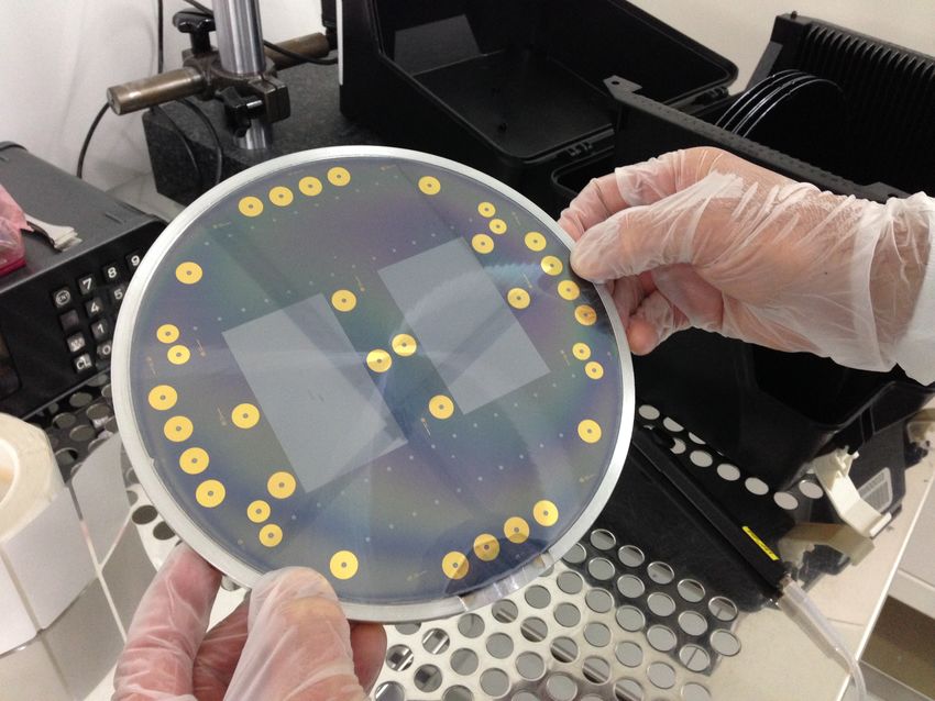
HOW DO WE MANUFACTURE SILICON MICROCHANNELS ?
▸ Collaborative effort between experiments (ALICE, LHCb and NA62),
 support groups (DT and ESE), and external partners (CSEM and EPFL).

 photolithography layout 8” wafer processed at CEA-LETI µchannels etching
 & Wafer Bonding

 Wafer Thinning

 cross-section of the cooling plates with embedded microchannels
 Silicon Etching
 DT Group Meeting, 22 June 2017 Alessandro Mapelli | 4
NA62 GTK - PIONEERING MICROCHANNELS !
▸ 2009 - concept of micro-cooling for the GTK presented Pπ
 to NA62: https://indico.cern.ch/event/58370/ PK

 2

 3
 1

 K_

 K_
 K_
▸ 2014 - First GTK in the experiment

 GT

 GT
 GT
 P
▸ 2016 - Data taking with 3 GTK detectors P
▸ 2017 - Assembly of 6 GTK modules for 2018 13 m 9m

 GTK_3
 9m
 GTK_2

 13m

 GTK_1
 Jordan DEGRANGE Jerome NOEL

 Diego ALVAREZ FEITO contributed to the design of the module

 The beam and detector of the NA62 experiment at CERN, Journal of Instrumentation, Volume 12, May 2017, https://goo.gl/P391U3

 DT Group Meeting, 22 June 2017 Alessandro Mapelli | 5
LHCb VELO UPGRADE - EVAPORATIVE CO2 IN MICROCHANNELS
 Feature Current VELO Upgraded VELO
 Sensors
 # of modules ▸ Primary heat source due to the VeloPix chips (~1 W/cm2)
 R & strips
 42
 0.22 m2
 Pixels
 52
 0.12 m2
 ▸
 Detector Active area

 Technology
 Sensors must be kept at -20ºC
 ⇠172k strips
 electron collecting
 ⇠41M pixels
 electron collecting

 Max fluence ▸ Evaporative CO2 circulates in microchannels routed directly under the VeloPix chips.
 300 µm thick
 3.9 ⇥ 1014
 200 µm thick
 8 ⇥ 1015

 ▸
 MeV · neq /cm 2 MeV · neq /cm 2
 HV tolerance
 ASIC Readout rate
 Total power consumption > 2kW.
 500 V
 1 MHz
 1000 V
 40 MHz
 Total data rate
 ▸ 52 modules in secondary vacuum separated by primary beam vacuum by a 0.25
 Total Power consumption
 ⇠150 Gb/s
 ⇠ 1 kW
 1.2 Tb/s
 2.2-2.3 kW

 mm thick Al foil.
 Table 1: An outline of the major di↵erences between the current VELO and its
 upgrade

 ▸ 24 cooling plates delivered by CEA-Leti. 20 more will be delivered within 2 months.
 ▸ Void-less soldering of connector to cooling plates procedure under development.
Figure 2: (top) Schematic of one half of the VELO upgrade detector. Twenty-
six modules are aligned along the beam direction. (bottom) Two modules in the
closed position. The modules are in di↵erent z-positions along the beam line to
minmise gaps in the acceptance and there is a slight overlap between the two
halves which aids detector alignment.
 c Copyright NIKHEF: reproduced with permission

rection, with the full length of the detector being approximately
1m. A module is made of two half-disc sensors with R- and
 -measuring geometry.

3. VELO Upgrade
 Figure 3: 3D Impact Parameter resolution vs particle inverse transverse mo-
 The Vertex Locator upgrade [3] is a significant redesign from mentum. Made using LHCb software simulation. A significant resolution im-
the original detector. The major changes in new detector and its provement of the upgraded detector (red) can be seen over the current VELO
 (black). The upgrade operates closer to the beam line and has a lower material
predecessor are as follows: budget - two major contributions to the improved resolution.
 c Copyright CERN: reproduced with permission
 • The detector will change from a silicon strip detector to a
 pixel detector.
 budget with thinner sensors and and thinner aluminium foil
 • The detector will be closer to the beam in its closed posi-
 housing each detector half and (ii) placing the sensors closer
 tion at 5.1 mm from 8.2 mm
 to the beam. The closer placement of the detector modules to
 • The upgraded VELO will use a new VeloPix ASIC [6] that the beam and the higher luminosity for LHC Run III comes with
 can be read out at 40 MHz (up from 1.1 MHz) and a band- some costs - the detector must be able to handle higher radiation
 width of up to 20.4 Gb/s. doses; there is a higher hit occupancy due to increased particle
 flux. This, in turn, results in higher data rates from the detector
 • The current detector modules are cooled with CO2 pass- and greater power consumption in the front-end ASICs (how-
 ing through a series of cooling blocks attached to the base ever, the dominant increase in data rate is due to the removal of
 of the module substrate. The upgraded modules will also the L0 hardware trigger). Table 1 lists some of the major di↵er-
 use CO2 as a coolant, but it will pass through micro- ences between the current VELO detector and the upgrade.
 channels in a silicon substrate, directly beneath the major
 heat sources (VeloPix ASICs and other chips). 3.1. Modules
 The upgraded VELO (shown in figure 2) will have more ro- A mechanical module concept is shown in figure 4. The cur-
bust track reconstruction performance compared to a strip de- rent design of the module consists of a carbon-fibre structure
tector and an overall improved resolution (figure 3). This im- supporting a silicon microchannel substrate. Stress-relieved
proved performance is achieved by (i) lowering the material CO2 cooling pipes route the CO2 to and from the cooling con-
 2
 SILICON COOLING PLATE MOCKUP
 WITH CONNECTOR AND CAPILLARIES

 DT Group Meeting, 22 June 2017 Alessandro Mapelli | 6
SILICON THERMAL MOCKUPS
 heater microchannel
 Resistive Temperature Detector
microfluidic inlet microfluidic outlet

 inlet capillary outlet manifold
 soldering pad
soldering pad

▸ Timothée FREI, PhD EPFL, 2021
 ▸ processing at CSEM on 6” wafers
▸ Désirée HELLENSCHMIDT, PhD
 ▸ post-processing at EPFL of 6” wafers from FBK
▸ Ranit MONGA, Intern, 2017
 ▸ processing at EPFK on 4” wafers

 DT Group Meeting, 22 June 2017 Alessandro Mapelli | 7

INTEGRATING MICROCHANNELS ON PIXEL DETECTORS
 ▸ Development of large-area monolithic detectors
 ▸ Embed microchannels on the backside of CMOS wafers
 “LOW TEMPERATURE” WAFER BONDING BURIED CHANNELS
 CEA-Leti, EPFL, G-Ray EPFL, FBK

 COOLING PLATE EMBEDDED MICROCHANNELS COOLING PLATE EMBEDDED MICROCHANNELS

 trenches - anisotropic etch trenches - anisotropic etch
 channels - anisotropic etch channels - anisotropic etch

arch - Zurich
 channels - isotropic etch channels - isotropic etch
quid Cooled Integrated Micro
 Micro-channel
 channel Heat Sinks
 wafer bonding wafer bonding

Figure of Merit:
 q
 COP
 P
 trench filling trench filling
 Heat Flux:
 Tj,max Tf,in
 q Achip
 Rtot

 Pumping Power
 P V p

 D.B. Tuckerman
 Tuckerman D.B. andand R.F.W.
 Pease Pease,
 R.F.W., IEEE
 IEEE Elec.
 Elec. Dev.Dev.
 Letters, Vol. 2, 5,Letters,
 1981. Vol. 2, 5, 1981

 Jacopo BRONUZZI, PhD EPFL, 2018
 Monday, October 11, 2010 © 2009 IBM Corporation
 Clémentine LIPP, MSc EPFL, 2017
 DT Group Meeting, 22 June 2017 Alessandro Mapelli | 8
jectives and Aims
 INTERCONNECTIVITY - DAISY CHAINING MICROFLUIDICS
 esent work was carried out in the framework of the development of a silicon
 ▸ NA62, LHCb
 Proposal by Miranda VAN STENIS
hannel-based cooling solution for the ALICE ITS. In order to illustrate the objectives
 1/16 SS pipe LASER soldered
 to KOVAR
ms of the work, an overview of a stave (i.e. the basic subcomponent ofMasterthe
 ▸ limited surfaces
 Thesis ITS) Development of an in plane microfluidic interconnect
 (CTE 6 ppm/K)
 Tiago Morais
 Cu 21mm for the thermal management of particle detectors
 plating
ng such a cooling solution is shown in Figure NA62
 5. Basically, it is composed Aof 1-kilosilicon
 ▸ access from the side
 2
 weight was used to press the syringe piston which has a surface of 550 mm . The
 SnPb pressure at the syringe is calculated as follows:
used to track the particles
 0.1 mm Foil resulting from collisions) glued to a silicon frame containing 1 ∗ 9.81

 ▸ alarger surfaces
 Au 100 nm −2
 Ni 350 nm 3.6mm = =

 =
 550
 = 1.78 ∗ 10

 = 178 2

hannels. A coolant Ti 200isnmsupplied to the microchannels through a connector, and
 The test is considered successful if water starts filling the cup and no drop of water is observed

 are▸ interconnections
 illepaM.A

 Silicon on or around the sample after 5 minutes of water circulation.
 fibre structure stiffens the assembly (furtherLHCb details on the layout of the Two
 (CTE 3 ppm/K)
 stavedifferent samples were tested with this procedure, they both circulate water. All the
 remaining samples were tested previously without using the outlet clamping. When pressing
n section 3). the syringe, drops of water flowed from the free outlet.

 In addition, some samples were cut near the connector, as shown in Figure 5.2 a), to allow
 imaging of the interior of the interconnect.

 igure 5 : Exploded-view of a stave for the ALICE ITS, including a silicon microchannel-based cooling system.
 Figure 5.2 a) Test sample with dicing path in red and cross-section orientation, b) Cross-
 DT Group Meeting, 22 June 2017 Alessandro
 sectional SEM image of the sample showing the two layers (Borofloat Mapelli
 33 and silicon) and|the9
 interconnect
SUMMARY & OUTLOOK
▸ Inter-disciplinary efforts are required to develop, fabricate and operate
 microsystems and microfluidic devices.
 ▸ DT is the perfect environment for such developments.
 ▸ The NA62 GTK modules and LHCb Velo cooling plates involve
 expertise from every section of the group.

▸ NA62 GTK - fabrication of cooling plates, assembly of modules and
 installation in the experiment.
▸ LHCb Velo - fabrication of the cooling plates and development of the
 soldering procedure for the connector.

▸ Silicon thermal mockups design and fabrication guidelines.
▸ Better integration of services in silicon sensors by embedding
 microchannels.
▸ Microfluidic interconnections to daisy chain cooling plates for staves
▸ Microfluidic closed-loop heat pipes for space applications.

 DT Group Meeting, 22 June 2017 Alessandro Mapelli | 10
You can also read